
 Open Access Article
 This Open Access Article is licensed under a Creative Commons Attribution-Non Commercial 3.0 Unported Licence
Study of the morphological, optical, structural and electrical properties of silicon nanowires at varying concentrations of the catalyst precursor†
Sadhna
Rai
a,
Rabina
Bhujel
a,
Manas Kumar
Mondal
b,
Bibhu Prasad
Swain
 *c and
Joydeep
Biswas
*d
*c and
Joydeep
Biswas
*d
aCentre for Materials Science and Nanotechnology, Sikkim Manipal Institute of Technology, Sikkim Manipal University, Majhitar, 737136, East Sikkim, India
bDepartment of Metallurgical and Materials Engineering, National Institute of Technology Durgapur, Durgapur 713209, India
cDepartment of Physics, National Institute of Technology, Manipur, Langol 795004, Manipur, India. E-mail: bibhuprasad.swain@gmail.com; bpswain@nitmanipur.ac.in
dDepartment of Chemistry, Sikkim Manipal Institute of Technology, Sikkim Manipal University, Majhitar, 737136, East Sikkim, India. E-mail: joyiisc@gmail.com; joydeep.biswas@smit.smu.edu.in
First published on 7th February 2022
Abstract
Silicon nanowires (SiNWs) were grown by metal-assisted chemical etching of a p-type (100) silicon wafer. AgNO3 was used as a precursor for the metal catalyst (Ag). The concentration of AgNO3 was varied for studying the properties of SiNWs. SiNWs with the longest length (11.49 μm) and smallest diameter (55.05 nm) were obtained by using 20 mmol of AgNO3 (20S). Their optical properties were studied using UV-Vis spectroscopy. The SiNWs showed space charge limited conduction characteristics. An ideality factor and a barrier height of 2.92 and 0.93 eV, respectively, were obtained for the 20S sample.
Introduction
Nanostructures have benefits over their bulk counterparts in several aspects such as phonon, photon and electron confinement. One dimensional (1-D) nanostructures viz., nanorods,1,2 nanowires3–5 and helical structures6 show interesting morphologies, structures and properties. Thus, they are used for application in sensors,7–9 and biomedical,10,11 energy storage12–14 and optoelectronic devices.15–17 One such trending material explored in recent years is silicon nanowires (SiNWs). They show improved properties compared to bulk Si because of the quantum confinement effect. Due to their improved optical and electronic properties, they are widely studied for their application in nano-optoelectronic devices.18,19The properties of SiNWs can be tailored by controlling their length, diameter and density. The bandgap in SiNWs can be tuned by varying various parameters. Kurokawa et al. reduced the diameter of SiNWs for tuning the bandgap.20 A bandgap value of 1.2 eV for SiNWs of diameter 30 nm was obtained. Wendisch et al. used MACE and KOH etching to control the microstructure of the SiNWs.21 Bisegmented nanowire arrays were generated using such a technique. These nanowires showed enhanced optical properties with controllable light absorption. Rahmani et al. varied the etching duration of Si to study the optical and electrical properties of the SiNWs.4 For an etching time of 30 s, the SiNWs showed a broad band in photoluminescence spectra. It showed a rectifying behaviour with an ideality factor of 2.8.
Various methods are used to fabricate SiNWs, such as vapour–solid–liquid (VLS) growth,18 chemical vapour deposition (CVD),22 molecular beam epitaxy (MBE),23 and laser ablation.24 However, these processes require sophisticated equipment. For the growth of SiNWs using these processes, high temperature and pressure have to be maintained. The overall cost of the production of SiNWs thus increases. In addition, the growth of nanowires is limited to a small area. These limitations can be overcome using a simple and cost-effective method, i.e., electroless metal-assisted chemical etching (EMACE).25
Over the years, researchers have made several modifications in EMACE to fabricate SiNWs. There are several factors on which the fabrication of SiNWs depends. Firstly, it depends on the type of metal catalyst used, its shape and the direction of movement.26,27 Secondly, it depends on the concentration of the etching solution (H2O2 and HF).28,29 Thirdly, the temperature also influences the growth of the nanowires.30 Lastly, the orientation of Si controls the direction of growth of the nanowires.31
Another critical factor that affects the fabrication of SiNWs is the metal catalyst concentration. Several groups of researchers have synthesised SiNWs by varying the concentration of AgNO3 viz., Cao et al.,32 Venkatesan et al.,32 Ozdemis et al.,33 and Velez et al.34 However, their investigation was limited to the geometry and reflectance characteristics of the SiNWs. The other properties, such as the structural and electrical properties, were unexplored. In the present study, the SiNWs are synthesised by varying the concentration of AgNO3. We present a detailed study of the structural and electrical properties in addition to the morphological and optical properties of the SiNWs.
Experimental details
Cleaning of silicon wafers
The p-type Si wafers (p-Si) (orientation: 〈100〉, thickness: 525 ± 25 μm, resistivity: 1–10 Ω cm) were cleaned following the RCA cleaning procedure. The schematic for the cleaning process is given in Fig. S1 (ESI†).Synthesis of SiNWs
The RCA cleaned p-Si wafer was then electroplated by dipping in a solution containing 20 mmol AgNO3 and 4.8 M HF. During this time, the Ag nanoparticles formed on the surface of Si. The wafer was removed and placed directly into an etching solution of 0.8 M H2O2 and 4.8 M HF. It was left in this solution for 15 min to form SiNWs. Lastly, it was removed and placed in concentrated HNO3 for 30 min to remove the Ag nanoparticles. The same procedure was followed to optimise the etching time, viz., 30, 45 and 60 min.The optimum etching time was found to be 45 min after the SEM analysis. Now, in the electroplating step, the concentration of AgNO3 was varied as 10, 20 and 30 mmol. The rest of the procedure was the same as above. The samples were named 10S, 20S and 30S, respectively.
Characterisation studies
The FESEM images and EDX spectra were obtained using a Carl Zeiss SIGMA equipped with an Element, AMETEK detector. AFM measurements were recorded on an INTEGRA (NT-MDT-INTEGRA). Raman spectra were obtained using a Horiba Jobin Yvon (HR800-UV confocal) micro-Raman spectrometer using an excitation wavelength of 532 nm. UV-Vis spectra were recorded on an Agilent Technologies, Czcerny 100 UV-Vis spectrophotometer. The sample size was 2.5 cm × 2.5 cm and the scanning rate was 600 nm min−1. The current–voltage (I–V) measurements were done using a KEYSIGHTB2901A source meter attached to the solar simulator (Class AAA), Model SS F5-3A with integrated Iris model: SS-O-Iris.Results and discussion
Mechanism
The etching of the p-Si wafer was carried out in two steps, as shown in Fig. 1. In the first step, the RCA cleaned p-Si wafer was subjected to electroplating by Ag nanoparticles. The Ag+ ions are reduced on the surface of Si. Since Ag is more electronegative than Si, it extracts electrons for the valence band of Si. Thus, it reduces Ag+ to give Ag particles and accumulates holes below it. The Ag particles then act as a catalyst in the etching of Si. Si is oxidised to SiO2, further etched away by HF as H2SiF6.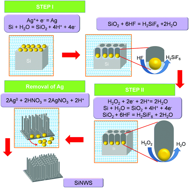 | ||
| Fig. 1 Schematic illustration and mechanism for the synthesis of SiNWs using two step MACE. | ||
In the second step, the electroplated Si is immersed in an aqueous solution of HF and H2O2. The interface between the AgNPs and SiNWs acts as the half cell where the galvanic exchange takes place between the Ag nanoparticles and Si wafer, as shown in Fig. 1. In the process, Ag+ receives an electron from Si to form Ag. As Ag+ is reduced, the Si below the Ag particles is oxidised to SiO2. The SiO2 is then etched away by HF as soluble H2SiF6. The Ag particles are again oxidised by H2O2 to Ag+ ions. The cycle is repeated until the wafer is removed from the etching solution, as shown in Fig. 1. Lastly, the Ag particles are removed by HNO3. The Ag particles react with HNO3 to form AgNO3 again, washed away by water.
Optimisation of etching time
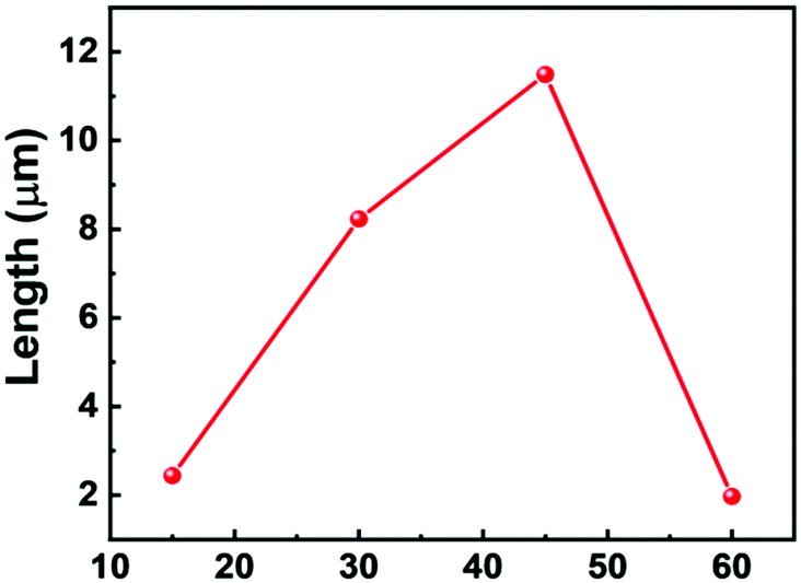
First, the clean p-Si wafer was electroplated in a solution containing a 20 mmol AgNO3 and a 4.8 M HF solution for 60 s. The silicon wafer was then etched at various etching times viz., 15, 30, 45 and 60 min. The FESEM images of the respective SiNWs are shown in Fig. 2. The length of the nanowires was measured using Image J software. A plot of nanowire length versus the etching time is given in Fig. 3. The length of the nanowires increased with an increase in the etching time. A similar trend was observed in previous studies by other researchers viz., Doudi et al.35 and Gaidi et al.36 With the increase in etching time, the topology of the nanowires also changed. As the length of the nanowires increase, they become more flexible and bending takes place. As a result, the tips are flocked together due to van der Waals attractive force.36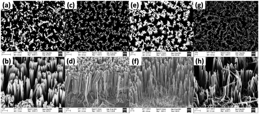 | ||
| Fig. 2 Top and cross-sectional view FESEM images of SiNWs etched at (a and b) 15 min, (c and d) 30 min, (e and f) 45 min and (g and h) 60 min. | ||
 | ||
| Fig. 3 Etching time versus time plot for SiNWs. | ||
However, the length of the nanowires decreased drastically at 60 min. This may be because the silicon wafer was exposed to etching solution for too long, which led to excessive etching of the Si wafer. This excessive etching resulted in snapping of the nanowires as seen in Fig. 2g and h. The longest length was achieved at 45 min.
Variation of the concentration of AgNO3
Furthermore, taking 45 min as the optimum time, the concentration of AgNO3 was varied. In Fig. 3, the low and high magnification FESEM images of Ag nanoparticles deposited on p-Si are shown. From the mechanism, we saw that the nucleation of Ag nanoparticles on the Si wafer takes place as p-Si is dipped in the aqueous solution of AgNO3/HF. Here, the authors have varied the concentration of AgNO3, viz., 10, 20 and 30 mmol, named 10A, 20A and 30A, respectively.The FESEM image of 10A (Fig. 4a) shows that the Ag nanoparticles are densely formed on the surface of p-Si. In the magnified image (Fig. 4b), it is seen that the nanoparticles possess a spaghetti-like structure. As the concentration of the AgNO3 is increased to 20 mmol, the Ag nanoparticles start to agglomerate together (Fig. 4c) in 20A. With the increase in the concentration of salt, the nucleation is more and the Ag nanoparticles are agglomerated together, leading to the formation of dendrites in addition to spherical nanoparticles (Fig. 4d). At the maximum concentration of 30A, rod-like structures are also visible in addition to spherical nanoparticles (Fig. 4e). Since no factor is known to control the growth of the Ag nucleus, the agglomeration takes place in random directions and hence different morphologies are observed.
 | ||
| Fig. 4 FE-SEM images at different magnifications for 10A (a and b), 20A (c and d) and 30A (e and f). | ||
The EDX analysis and elemental mapping of 10A, 20A and 30A are presented in Fig. S2 (ESI†). The percentage composition of Ag increased as the concentration of AgNO3 was increased. The lowest and highest percentage of Ag is observed for 10A and 30A, respectively. In the case of 20A, some percentage of oxygen is also present. It may be due to the formation of Ag2O by the reaction of Ag with the atmospheric oxygen.
Again, the morphology of the Ag NPs formed on the p-Si was studied using AFM. In Fig. S3a (ESI†), Ag nanoparticles show minimum agglomeration and the particles are quite distant from one another. However, the Ag NPs are agglomerated more in the case of 20A. The NPs are less distant from one another and densely formed on p-Si (Fig. S3b, ESI†). In some places, the NPs are separate and in other places, they come together to form lumps. The Ag NPs are most dense in the case of 30A (Fig. S3c, ESI†). The Ag NPs are clumped together; and as a result, they form a rod-like structure. The results were the same as those observed from FESEM analysis. The average roughness values for 10A, 20A and 30A are 0.275, 2.097 and 2.318 μm, respectively. The roughness values increased as the concentration of AgNO3 was increased.
From the top view of the FESEM images of the SiNWs, it is observed that for the nanowires in 10S the tips of the nanowires are not separated properly. In this case, nanoparticles have hole formation, as shown in Fig. 5a and b. Since the atomic% of Ag was low, this amount was not enough to form well-separated nanowires. As the concentration is increased to 20 mmol, though some agglomeration is present, most of the nanowires are well-formed and the tips are separated (Fig. 5d and e). In this case, free-standing and vertical nanowires are formed as seen in the cross-sectional view of the FESEM image (Fig. 5f). However, when the concentration increases to 30 mmol, the nanowires are deformed. At 30 mmol large rod-shaped and agglomerated Ag particles were formed, as seen in Fig. 4e.
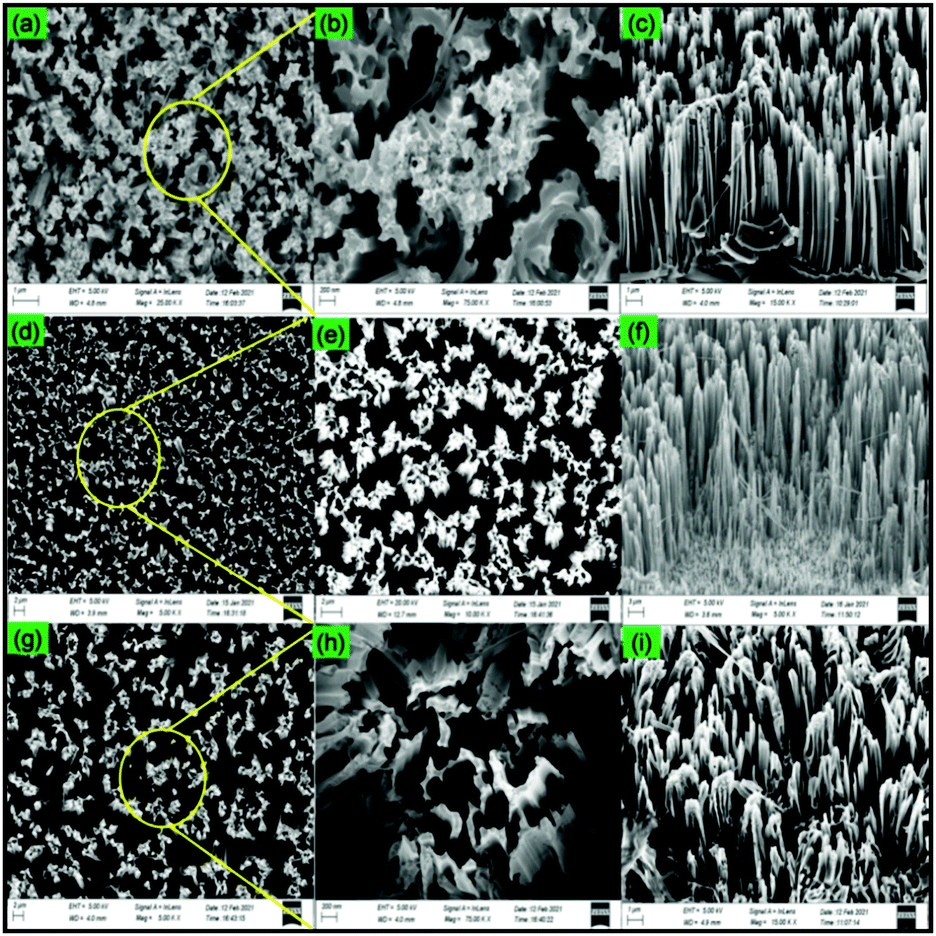 | ||
| Fig. 5 Top view FESEM images of (a) 10S, (d) 20S, (g) 30S and their magnified images (b, e and h). Cross-sectional FESEM images of (c) 10S, (f) 20S and (g) 30S. | ||
These particles may have led to the formation of large holes. Also, the high content of the Ag catalyst led to the excessive oxidation of Si, leading to uncontrolled etching of the Si. Hence, at 30 mmol well-defined SiNWs were not formed (Fig. 5i).
From the cross-sectional view of the SEM images of 10S, 20S and 30S, the lengths of the nanowires were measured. For this purpose, Image J software was used. The average values of the length of the SiNWs are provided in Table 1. The length of nanowires increases in the order 30S < 10S < 20S. The longest length is that for 20S, i.e., 11.49 μm. From the FESEM analysis, it is found that well defined vertical SiNWs with the longest lengths are synthesised at 20 mmol of AgNO3.
| Sample code | Length (μm) | Diameter (nm) | R a (μm) | R s (μm) |
|---|---|---|---|---|
| The Ra and Rq values are maximum for 30S, which shows minimum uniformity. In contrast, these values are minimum for the 20S sample, indicating maximum uniformity. This was also seen from the SEM and AFM images. Similar results were observed by Chhetri et al.37 | ||||
| 10S | 5.86 | 63.94 | 3.72 | 0.674 |
| 20S | 11.49 | 55.05 | 0.97 | 0.263 |
| 30S | 3.11 | 88.16 | 3.94 | 1.21 |
The elemental mapping and the EDX spectra for 10S, 20S and 30 S are presented in Fig. S4 (ESI†). The elements present and their weight% and atomic% are shown in the EDX spectra. The main elements present are Si and O. A small amount of Ag is present in the 20S due to the formation of Ag2O formed in the electroplating process. This was not removed even after washing in HNO3.
From the AFM images of SiNWs (Fig. 6a–d), it is clear that 10S and 30S show agglomeration, whereas 20S shows well-defined nanowires. The diameter of the nanowires was calculated using the Gwyddion software. To measure the diameter, a line was drawn diagonally across the 3D AFM images of the SiNWs using a feature in the application called the line profile. Several peaks were then obtained. By taking the average of the width of the peaks, the diameter of the nanowires was obtained. The line profile of the peaks obtained after drawing the diagonals is shown in Fig. S6 (ESI†). The average diameters of the nanowires are provided in Table 1. The 20S showed the smallest value for the diameter, i.e., 55.05 nm. As seen from the SEM and AFM images, 10S and 30S showed higher diameter values because the NWs were agglomerated together. The values for average roughness (Ra) and root mean square roughness (Rq) were obtained from Gwyddion. The values are incorporated in Table 1.
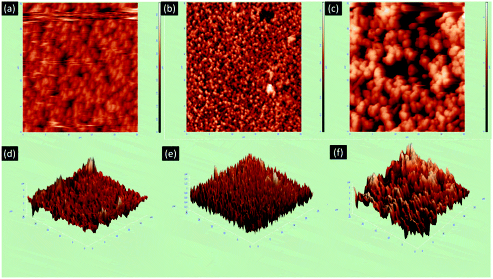 | ||
| Fig. 6 2D and 3D AFM images of (a and d) 10S, (b and e) 20S and (c and f) 30S respectively. | ||
Optical properties
The optical properties of silicon nanowires were studied using diffuse surface reflectance analysis. The reflectance for SiNWs was measured in the range of 200 to 800 nm (Fig. 7). The reflectance for SiNWs is observed to decrease in the range of 300 to 400 nm (UV region). In this range, the reflectance for 30S was minimum (4.06%). However, the reflectance increases gradually in the range of 400 to 800 nm (visible region). Finally, at 800 nm, the reflectance for the 20S sample (15.39%) is lower than those for 10S and 30S. The nanowires show different values of reflectance at different wavelengths. Hence, the values of maximum reflectance (Rmax) and minimum reflectance (Rmin) in the UV and visible range are extracted and compiled in Table 2. The difference in the reflectance values for SiNWs may be due to various reasons such as length,38 diameter,39 shape, density40 and porosity41 of the nanowires.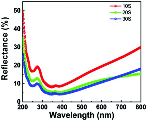 | ||
| Fig. 7 Reflectance spectra of 10S, 20S, and 30S. | ||
| Sample code | UV region | Visible region | ||
|---|---|---|---|---|
| R max (%) | R min (%) | R max (%) | R min (%) | |
| 10S | 8.13 | 19.17 | 8.73 | 30.00 |
| 20S | 5.26 | 13.12 | 5.35 | 15.39 |
| 30S | 4.06 | 9.82 | 4.35 | 18.06 |
Structural properties
Fig. 8 presents the Raman spectra of Si and the SiNWs synthesised using different concentrations of AgNO3. These spectra were obtained using an excitation wavelength of 532 nm and a power of 50 mW. The signature peak for planar Si is centered at 520.7 cm−1.42 However, for the SiNWs, a redshift is observed for all the samples with a broadening of the peak. The peaks of 10S, 20S and 30S are centered at 515.8, 518.3 and 519.3 cm−1, respectively. The redshift may be due to the phonon confinement.25 The nanowires have a large surface area compared to the bulk Si. Hence, an increase in the intensity of the peaks for SiNWs has been observed in Fig. 8.43 The SiNWs with longer lengths showed higher intensity. Similar results were observed by Rodichkina et al.44 The increased intensity may be due to the enhanced transmission excitation.25 The higher intensities of the Raman spectra suggest that the SiNWs are highly crystalline.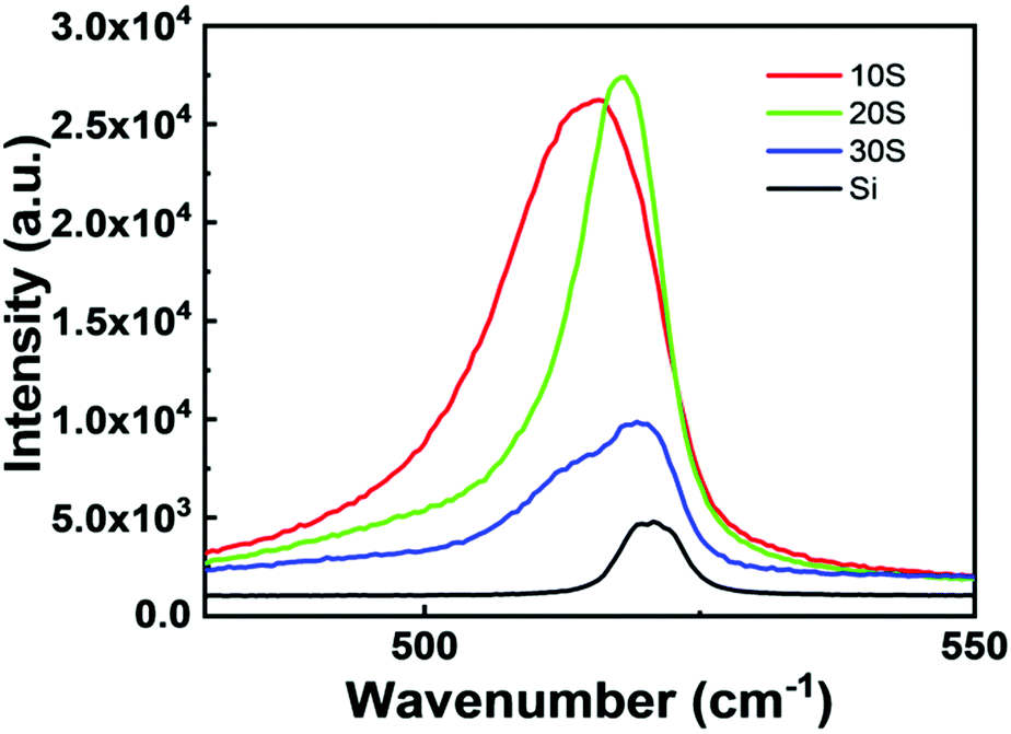 | ||
| Fig. 8 Raman spectra of Si, 10S, 20S and 30S. | ||
The full width at half maximum (FWHM) value for p-Si was 7.84 cm−1. However, the peaks for the SiNWs were broadened, showing FWHM values of 18.11, 10.35 and 16.92 nm for 10S, 20S and 30S, respectively. The peak broadenings for the nanowires with larger diameters are more than those with smaller diameters. 20S has the smallest diameter (55.05 nm) as calculated from AFM and has the lowest value of FWHM.
Electrical properties
The front contact was made on Si and SiNWs using Ag paste to measure the electrical properties. The dark and photocurrent measurement was done in a solar simulator. The I–V measurements were done by applying a bias from −3 to 3 V. The photocurrent was obtained by illuminating the samples under 1 Sun irradiation. The dark and photocurrent responses of Ag/Si and Ag/SiNW/Si are shown in Fig. 9. It is observed that the current is the lowest for Ag/Si under both dark and light conditions. The reason is that the planar silicon has an indirect bandgap. When planar Si is converted to nanowires, the indirect bandgap changes to the direct bandgap facilitating the easy movement of electrons. Also, SiNWs have a lower reflectance value than planar Si. The more the light absorbed, the more its utilisation for electron excitation, increasing the current. Among the SiNWs, Ag/20S/Si shows the highest current under illumination. This is because it has the lowest reflectivity seen from UV-Vis spectroscopy. It has the smallest diameter and longest length. So, it has the highest ability to trap light. In addition, the mobility of the charge carrier in the case of SiNWs depends on the diameter of the nanowires. The smaller the diameter, the higher the mobility.45 This also explains the higher current response of the Ag/20S/Si.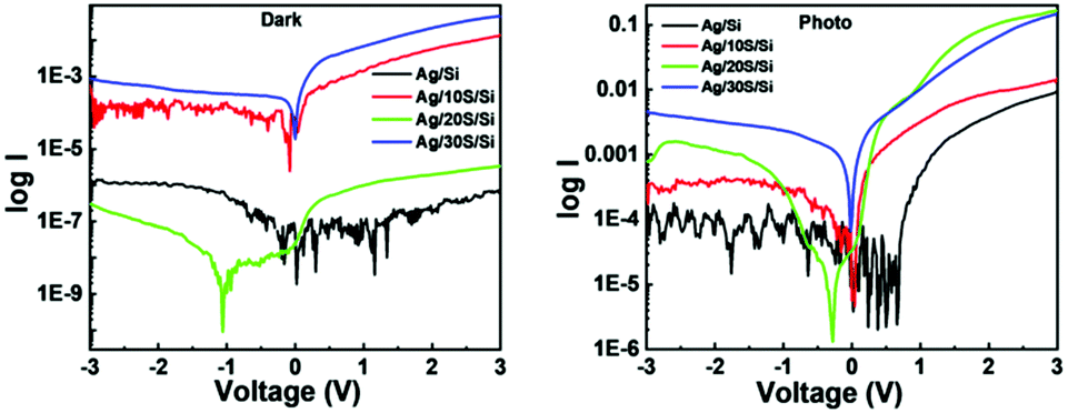 | ||
| Fig. 9 Dark and photo current response of Ag/Si, Ag/10S/Si, Ag/20S/Si and Ag/30S/Si. | ||
All the samples show diode characteristics with rectification characteristics. The rectification ratio is calculated by dividing the current in forwarding bias by reverse bias at the same voltage. The rectification ratios of Ag/10S/Si, Ag/20Si and Ag/30S/Si samples are listed in Table 3. The diode Ag/20S shows the highest rectification ratio of 83.50 at 2 V.
| Sample code | Rectification ratio | Ideality factor | Barrier height (eV) |
|---|---|---|---|
| Ag/Si | 1.25 | 0.31 | |
| Ag/10S/Si | 23.18 | 3.93 | 1.06 |
| Ag/20S/Si | 83.50 | 2.92 | 0.93 |
| Ag/30S/Si | 16.66 | 2.42 | 1.21 |
The ideality factor (η) and barrier height (φb) of a Schottky diode is calculated using the following equations46
 | (1) |
 | (2) |
Here, a and A* refer to the effective area of the diode (1 cm2) and Richardson's constant (32 A cm−2 K−2 for p-Si).
The ideality factor and barrier height values calculated from the I–V plot is presented in Table 3. The ideality factor and barrier height of the Ag/Si is 1.25 and 0.31 eV, respectively. It is evident that the η values decrease with the increase in the concentration of AgNO3. The ideality factor observed in this study is considerably lower than that obtained by Wang et al. (3.51 to 4.62)47 and Rahmani et al. (2.8 to 5.4).4 The deviation of the ideality factor from unity may be due to the presence of an oxide layer in SiNWs.48
The barrier height of the SiNWs decreased with the decrease in their diameter. The barrier height of the 20S is observed to be the lowest since it has the smallest diameter. The result of the present study is consistent with the results in the literature. Several reasons have been proposed for the dependency of the diameter of nanowires on the barrier height viz. electron–hole recombination in the depletion region,49 the presence of interface states in the nanowires,50 the presence of positive charge around the nanowire and surface state density.51 The low value of Ag/Si may be due to lower recombination losses than the diodes for SiNWs. In the present work, the density of the nanowires increased as the diameter increased, which was observed in the FESEM analysis. Hence, the lower barrier height may be due to a larger density of nanowires with a smaller diameter. The decrease in the barrier height may also be attributed to the presence of the oxide layer and defect states in SiNWs. A similar result was observed in a recent work by Hu et al.48
Log![[thin space (1/6-em)]](https://www.rsc.org/images/entities/char_2009.gif) I versus logV was plotted to investigate the conduction mechanism in the SiNW samples, which is presented in Fig. 10. The behaviour of the junctions suggests that they follow the power-law I ∼ Vm, where m represents the slope of the curve. The 10S and 30S samples show two values of m. In the low voltage region, they show ohmic behaviour. In contrast, they follow the space charge limited conduction (SCLC) mechanism at a higher voltage. The SiNWs have a high surface to volume ratio. The surface states lead to the depletion of charge carriers. As a result, the trapped SCLC affects the charge transport.4
I versus logV was plotted to investigate the conduction mechanism in the SiNW samples, which is presented in Fig. 10. The behaviour of the junctions suggests that they follow the power-law I ∼ Vm, where m represents the slope of the curve. The 10S and 30S samples show two values of m. In the low voltage region, they show ohmic behaviour. In contrast, they follow the space charge limited conduction (SCLC) mechanism at a higher voltage. The SiNWs have a high surface to volume ratio. The surface states lead to the depletion of charge carriers. As a result, the trapped SCLC affects the charge transport.4
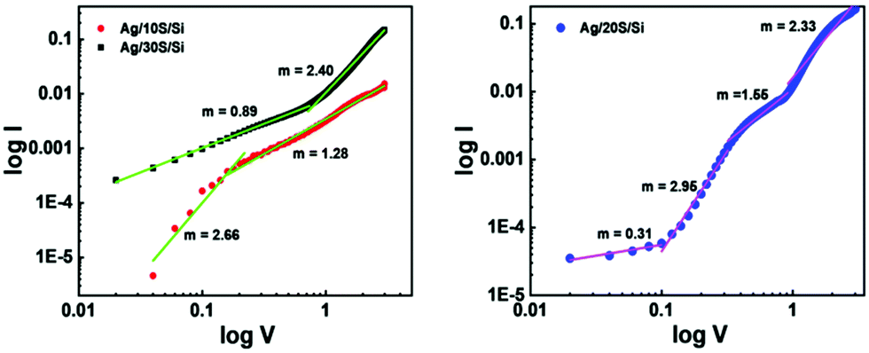 | ||
| Fig. 10 LogI vs. logV plot of Ag/10S/Si, Ag/30S/Si and Ag/20S/Si diode. m is the slope of the curve. | ||
Furthermore, in the case of 20S, four values of m are observed. The 20S sample shows Ohmic behaviour in the low voltage region, shallow trap SCLC followed by trap-filled limited SCLC in the medium voltage region and trap free SCLC regime at higher voltage region.52 The SiNWs follow the SCLC mechanism due to defect or trap states.53 As the density increases, the number of traps increases. So the different behaviour of the 20S sample may be because it has the highest density. Also, it has the highest oxygen content; as a result, there will be a large number of trapping states at the Ag/SiNW interface. The results show that the SiNW junctions transit from ohmic behaviour in the low voltage region to the SCLC behaviour in the high voltage region. Similar results were reported by other research groups working with SiNWs.4,54
Conclusions
SiNWs were synthesised by following two step MACE. The concentration of AgNO3 was varied as 10, 20 and 30 mmol. The etching time was optimised as 45 min. The length and diameter of the nanowires were calculated from FESEM and AFM analysis, respectively. The 20S sample showed the longest length (11.49 μm) and smallest diameter (55.05 nm). The ideality factor and barrier were calculated from the I–V plot. For the 20S sample, the ideality factor and barrier height were calculated as 2.92 and 0.93 eV.Author contributions
Sadhna Rai: Conceptualisation, methodology, writing the original draft; Rabina Bhujel: Methodology and formal analysis; Manas Kumar Mondal: Formal analysis; Bibhu P. Swain: Supervision, review & editing; Joydeep Biswas: Supervision, review & editing.Conflicts of interest
On behalf of all authors, the corresponding authors state that there are no conflicts to declare.Acknowledgements
Ms Sadhna Rai acknowledges the UGC-DAE-CSR, Indore (Project Ref: CSR-IC-MSR-07/CRS-215/2017-18/1296), for a Grant-in-Aid for a Junior Research Fellowship. The authors acknowledge the Sophisticated Analytical Instrumentation Facility, IIT Bombay, for providing UV-Vis spectroscopy and Raman spectroscopy characterisation facilities. The authors also acknowledge the Centre of Excellence in Advanced Materials, NIT Durgapur, and Instrumentation Facility, IIT Roorkee, for their help in acquiring FESEM and AFM images, respectively.References
- Q. Chen, R. Zhu, S. Liu, D. Wu, H. Fu, J. Zhu and H. He, J. Mater. Chem. A, 2018, 6, 6356–6362 RSC.
- L. Schlur, J. R. Calado and D. Spitzer, R. Soc. Open Sci., 2018, 5, 180510 CrossRef PubMed.
- R. Bhujel, S. Rai and B. P. Swain, Mater. Sci. Semicond. Process., 2019, 102, 104592 CrossRef CAS.
- M. Rahmani, S. Amdouni, M. Zaïbi and A. Meftah, Silicon, 2021, 13, 179–187 CrossRef CAS.
- N.-H. Tran, T.-H. Duong and H.-C. Kim, Sci. Rep., 2017, 7, 15093 CrossRef PubMed.
- Z. Ren and P.-X. Gao, Nanoscale, 2014, 6, 9366 RSC.
- T. F. Choo, N. U. Saidin and K. Y. Kok, R. Soc. Open Sci., 2018, 5, 172372 CrossRef PubMed.
- L. Shahriary, S. K. Haram and A. A. Athawale, Talanta, 2013, 104, 212–218 CrossRef CAS PubMed.
- H. A. Wahab, A. A. Salama, A. A. El Saeid, M. Willander, O. Nur and I. K. Battisha, Results Phys., 2018, 9, 809–814 CrossRef.
- Y. P. Ivanov, A. Alfadhel, M. Alnassar, J. E. Perez, M. Vazquez, A. Chuvilin and J. Kosel, Sci. Rep., 2016, 6, 24189 CrossRef CAS PubMed.
- J. Xu, Y. Xue, J. Cao, G. Wang, Y. Li, W. Wang and Z. Chen, RSC Adv., 2016, 6, 5541–5546 RSC.
- V. H. Luan, J. H. Han, H. W. Kang and W. Lee, Composites, Part B, 2019, 178, 107464 CrossRef CAS.
- R. Kumar, A. Soam, R. O. Dusane and P. Bhargava, J. Mater. Sci.: Mater. Electron., 2018, 29, 1947–1954 CrossRef CAS.
- W. Pan, M. Zhang, F. Gui, Y. Han and X. Sun, Mater. Res. Bull., 2022, 145, 111549 CrossRef CAS.
- L.-B. Luo, X.-H. Wang, C. Xie, Z.-J. Li, R. Lu, X.-B. Yang and J. Lu, Nanoscale Res. Lett., 2014, 9, 637 CrossRef PubMed.
- M. Ding, Z. Guo, L. Zhou, X. Fang, L. Zhang, L. Zeng, L. Xie and H. Zhao, Crystals, 2018, 8, 223 CrossRef.
- Y. Li, F. Qian, J. Xiang and C. M. Lieber, Mater. Today, 2006, 9, 18–27 CrossRef CAS.
- M. Shao, D. D. D. Ma and S. Lee, Eur. J. Inorg. Chem., 2010, 4264–4278 CrossRef CAS.
- M. K. Sahoo and P. Kale, J. Materiomics, 2019, 5, 34–48 CrossRef.
- Y. Kurokawa, M. Yano, S. Miyajima and A. Yamada, Jpn. J. Appl. Phys., 2017, 56, 04CS03 CrossRef.
- F. J. Wendisch, M. Abazari, H. Mahdavi, M. Rey, N. Vogel, M. Musso, O. Diwald and G. R. Bourret, ACS Appl. Mater. Interfaces, 2020, 12, 13140–13147 CrossRef CAS PubMed.
- O. Demichel, F. Oehler, V. Calvo, P. Noé, N. Pauc, P. Gentile, P. Ferret, T. Baron and N. Magnea, Phys. E, 2009, 41, 963–965 CrossRef CAS.
- P. Werner, N. D. Zakharov, G. Gerth, L. Schubert and U. Gösele, Int. J. Mater. Res., 2006, 97, 1008–1015 CAS.
- V. Schmidt, J. V. Wittemann, S. Senz and U. Gösele, Adv. Mater., 2009, 21, 2681–2702 CrossRef CAS.
- R. Bhujel, U. Rizal, A. Agarwal, B. S. Swain and B. P. Swain, J. Mater. Eng. Perform., 2018, 27, 2655–2660 CrossRef CAS.
- K. A. Gonchar, V. Y. Kitaeva, G. A. Zharik, A. A. Eliseev and L. A. Osminkina, Front. Chem., 2019, 7, 1–7 CrossRef PubMed.
- F. J. Wendisch, M. Rey, N. Vogel and G. R. Bourret, Chem. Mater., 2020, 32, 9425–9434 CrossRef CAS PubMed.
- Y. Liu, G. Ji, J. Wang, X. Liang, Z. Zuo and Y. Shi, Nanoscale Res. Lett., 2012, 7, 663 CrossRef PubMed.
- A. Najar, A. B. Slimane, M. N. Hedhili, D. Anjum, R. Sougrat, T. K. Ng and B. S. Ooi, J. Appl. Phys., 2012, 112, 033502 CrossRef.
- O. Fellahi, T. Hadjersi, M. Maamache, S. Bouanik and A. Manseri, Appl. Surf. Sci., 2010, 257, 591–595 CrossRef CAS.
- Z. Huang, N. Geyer, P. Werner, J. de Boor and U. Gösele, Adv. Mater., 2011, 23, 285–308 CrossRef CAS PubMed.
- D. T. Cao, L. T. Q. Ngan, T. Van Viet and C. T. Anh, Int. J. Nanotechnol., 2013, 10, 343 CrossRef CAS.
- B. Ozdemir, M. Kulakci, R. Turan and H. E. Unalan, Nanotechnology, 2011, 22, 155606 CrossRef PubMed.
- V. Velez and K. Sundaram, Int. J. Nanosci. Nanotechnol., 2017, 13, 283–288 Search PubMed.
- K. Daoudi, K. Ramachandran, H. Alawadhi, R. Boukherroub, E. Dogheche, M. A. El Khakani and M. Gaidi, Surf. Interfaces, 2021, 27, 101454 CrossRef CAS PubMed.
- M. Gaidi, K. Daoudi, S. Columbus, A. Hajjaji, M. A. El Khakani and B. Bessais, J. Environ. Sci., 2021, 101, 123–134 CrossRef PubMed.
- N. Chhetri, S. Haldar and S. Chatterjee, Mater. Res. Express, 2020, 6, 1250i2 CrossRef.
- V. T. Pham, M. Dutta, H. T. Bui and N. Fukata, Adv. Nat. Sci.: Nanosci. Nanotechnol., 2014, 5, 045014 CAS.
- S. A. Razek, M. A. Swillam and N. K. Allam, J. Appl. Phys., 2014, 115, 194305 CrossRef.
- K.-Q. Peng and S.-T. Lee, Adv. Mater., 2011, 23, 198–215 CrossRef CAS PubMed.
- P. Parashar, D.-R. Jian, W. Huang, Y.-W. Huang and A. Lin, IEEE 44th Photovoltaic Specialist Conference (PVSC), 2017, 1631–1634.
- S. A. Mala, L. Tsybeskov, D. J. Lockwood, X. Wu and J.-M. Baribeau, J. Appl. Phys., 2014, 116, 014305 CrossRef.
- S. Weidemann, M. Kockert, D. Wallacher, M. Ramsteiner, A. Mogilatenko, K. Rademann and S. F. Fischer, J. Nanomater., 2015, 2015, 1–11 CrossRef.
- S. P. Rodichkina, L. A. Osminkina, M. Isaiev, A. V. Pavlikov, A. V. Zoteev, V. A. Georgobiani, K. A. Gonchar, A. N. Vasiliev and V. Y. Timoshenko, Appl. Phys. B: Lasers Opt., 2015, 121, 337–344 CrossRef CAS.
- J. Ramanujam, D. Shiri and A. Verma, Mater. Express, 2011, 1, 105–126 CrossRef CAS.
- M. Rahmani and A. Meftah, J. Mater. Sci.: Mater. Electron., 2020, 31, 16352–16359 CrossRef CAS.
- Z. Wang, M. Zhu, X. Chen, Q. Yan and J. Zhang, Microelectron. Eng., 2013, 103, 36–41 CrossRef CAS.
- X. F. Hu, S. J. Li, J. Wang, Z. M. Jiang and X. J. Yang, Nanoscale Res. Lett., 2020, 15, 52 CrossRef CAS PubMed.
- F. Léonard, A. A. Talin, B. S. Swartzentruber and S. T. Picraux, Phys. Rev. Lett., 2009, 102, 106805 CrossRef PubMed.
- K. Yoon, J. K. Hyun, J. G. Connell, I. Amit, Y. Rosenwaks and L. J. Lauhon, Nano Lett., 2013, 13, 6183–6188 CrossRef CAS PubMed.
- A. Soudi, C.-H. Hsu and Y. Gu, Nano Lett., 2012, 12, 5111–5116 CrossRef CAS PubMed.
- P. Zhang, Y. S. Ang, A. L. Garner, Á. Valfells, J. W. Luginsland and L. K. Ang, J. Appl. Phys., 2021, 129, 100902 CrossRef CAS.
- M. Rahmani, A. Moadhen, M.-A. Zaïbi, A. Lusson, H. Elhouichet and M. Oueslati, J. Alloys Compd., 2009, 485, 422–426 CrossRef CAS.
- M. Ahmad, K. Rasool, M. A. Rafiq, M. M. Hasan, C. B. Li and Z. A. K. Durrani, Phys. E, 2012, 45, 201–206 CrossRef CAS.
Footnote |
| † Electronic supplementary information (ESI) available. See DOI: 10.1039/d1ma01145f |
| This journal is © The Royal Society of Chemistry 2022 |