
 Open Access Article
 This Open Access Article is licensed under a Creative Commons Attribution-Non Commercial 3.0 Unported Licence
Hierarchical hollow metal nanostructure arrays for selective CO2 conversion†
James W.
Maina
 *a,
Jennifer M.
Pringle
a,
Joselito M.
Razal
a,
Stella
Aslanoglou
bcd,
Roey
Elnathan
bc,
Nicolas H.
Voelcker
bc and
Ludovic F.
Dumée
*ef
*a,
Jennifer M.
Pringle
a,
Joselito M.
Razal
a,
Stella
Aslanoglou
bcd,
Roey
Elnathan
bc,
Nicolas H.
Voelcker
bc and
Ludovic F.
Dumée
*ef
aGeelong, Institute for Frontier Materials, Deakin University, Waurn Ponds, Victoria, 3216, Australia. E-mail: j.maina@deakin.edu.au
bMelbourne Centre for Nanofabrication Victorian Node of the Australian National Fabrication Facility 151 Wellington Road, Clayton, VIC 3168, Australia
cMonash Institute of Pharmaceutical Sciences, Monash University, 381 Royal Parade, Parkville, Victoria 3052, Australia
dSchool of Physics, The University of Melbourne, Melbourne, Victoria 3010, Australia
eDepartment of Chemical Engineering, Halifa University, Abu Dhabi, United Arab Emirates. E-mail: ludovic.dumee@ku.ac.ae
fResearch and Innovation Center on CO2 and Hydrogen (RICH), Khalifa University, Abu Dhabi, United Arab Emirates
First published on 28th January 2022
Abstract
Metal hollow nanostructures have a wide range of potential applications in energy storage and conversion, owing to their low density, high surface to volume ratio, and high contact surface area. However, the fabrication of such nanostructures remains challenging to date, with most fabrication routes only limited to specific materials. Herein, a universal templating strategy for fabricating hierarchical and aligned arrays of hollow metal nanostructures, from a variety of metallic materials including Cu, Ag, Ni and Pd, is reported. By using copper as a representative material, it is demonstrated that these nanostructures exhibit an enhanced electrocatalytic activity for CO2 conversion, with the Cu nanostructures producing more than 205% and 183% higher yield for CO and H2 respectively, compared to non-nanostructured plain copper films at an applied potential of −2.4 V vs. Ag/AgCl. This work opens up a new route for fabricating hollow nanostructures with tailored metal compositions for energy storage and conversion applications.
Introduction
Hollow and porous metal nanostructures have a wide range of applications, ranging from catalysis, batteries, super-capacitors, plasmonics and solar cells, owing to their low density, high surface to volume ratio, and unique surface plasmon properties.1–8 As electrodes, the metal nanostructures provide larger contact surface area during electrochemical processes, reducing charge diffusion length and improving efficiency, while the inner voids suppress the destructive volumetric expansion and dendrite formation in lithium ion batteries, thereby improving the battery life.1,4 The ability to generate surface plasmons upon irradiation with light also makes hollow nanostructures promising for highly sensitive surface plasmon enhanced Raman spectroscopy and plasmon enhanced solar cells.2The reproducible and scalable manufacturing of hollow metal nanostructures, however, remains challenging to date.1 The most established fabrication methods are the hard and soft templating methods, whereby the metal is synthesized on the surface of ceramic, polymer or carbon templates, followed by selective removal of the sacrificial templates.2 Although these techniques were successfully employed for the fabrication of various metal oxide hollow nanostructures, such as ZnO, TiO2 and NiO microspheres,3,9 the fabrication of pure metals has been limited to a few select noble metal materials such as Pt, Au and Pd. Major limitations of this process are related to the harsh synthetic conditions, which require high temperature thermal annealing, leading to metal coalescence, as well as corrosive etching steps incompatible with most transition metals.1,9
An alternative method for the fabrication of hollow metal nanostructures is the galvanic replacement technique,10 which relies on the redox reaction, whereby a sacrificial metal template is selectively corroded by the ions of a secondary metal in solution, to produce hollow nanostructures composed of both metals.10–12 During the process, atoms present on the surface of the metal template become oxidized and are dissolved, while the metal ions of the secondary metal get reduced and deposit on the sacrificial metal template. Successful formation of the hollow nanostructures depends on the site selectivity of the crystal facets of the template, with corrosion taking place on sites that have high surface free energy, while the deposition of the secondary metal takes place on the areas of low surface energy.10 However, the galvanic reactions of transition metals is challenging to control due to the high surface free energy of the materials, leading to non-selective dissolution without simultaneous deposition of the secondary metal.10,12 As a result, the technique has also primarily been limited to the formation of noble metals based hollow nanostructures and much still remains to be done to develop hollow transition metal nanostructures.5,11
Furthermore, almost all techniques reported to date produced hollow nanostructures in a discrete form, such as spheres, nanocages and nanotubes, which require further assembly onto a supporting substrate or conductive electrode prior to application.1,5 This immobilization step may result in a number of undesirable effects, including non-structured agglomeration and clogging of the inner pores of the materials by binding agents, compromising their unique properties. Previous attempt to produce array of such nanostructures relied on electro-deposition technique,13,14 which would be difficult to reproduce across various metallic materials, or involved corrosive steps that would be incompatible with most transition metals.15 A universal technique to allow the formation of self-supporting arrays of the hollow nanostructures from different metallic materials is yet to be devised.
Herein, a general templating strategy and novel procedure for the fabrication of aligned arrays of self-supporting hollow metal nanostructures, from a variety of metallic materials including Cu, Ag, Ni and Pd, is reported. By using copper as a representative material, it is also demonstrated that such nanostructures exhibit an enhanced efficiency for the electrocatalytic conversion of CO2 to syngas (CO and H2), compared to non-nanostructured plain copper films under similar electrocatalytic conditions. This universal fabrication technique does not require any heat treatment or harsh chemical treatment, thus solving a major technical challenge for the fabrication of transition metal-based hollow nanostructures.
Results and discussion
The fabrication technique reported here involves three main steps, namely the design of silicon (Si) master mould, the preparation of polyvinyl alcohol template and then metal deposition (Fig. 1a). The master mould was prepared using deep reactive ion etching (DRIE) on a silicon wafer, which was precoated with a monolayer of poly(styrene) beads (Fig. S1, ESI†) to serve as a mask during the etching, thus enabling selective sculpturing of nano/micro patterns across the silicon surface.16 DRIE was carried out using the Bosch process,16,17 with sulfur hexafluoride (SF6) as the etchant gas and octafluorocyclobutane (C4F8) as the passivating gas. The etching process involved exposing the Si wafers alternately to SF6 and C4F8 gases for 24 cycles, leading to the formation of arrays of cylindrical micropillars with diameter of 2.60 ± 0.14 μm and height of about 7.50 μm (Fig. 1b). The obtained micropillars were then subjected to a pseudo-Bosch etching step by exposing the substrate simultaneously to SF6 and C4F8 gases in the absence of the PS mask. This action sharpened the tips, resulting in an array of cone-shaped Si nanostructures, with a tip diameter of 201 ± 6 nm and a height of 6.0 ± 0.8 μm (Fig. 1c).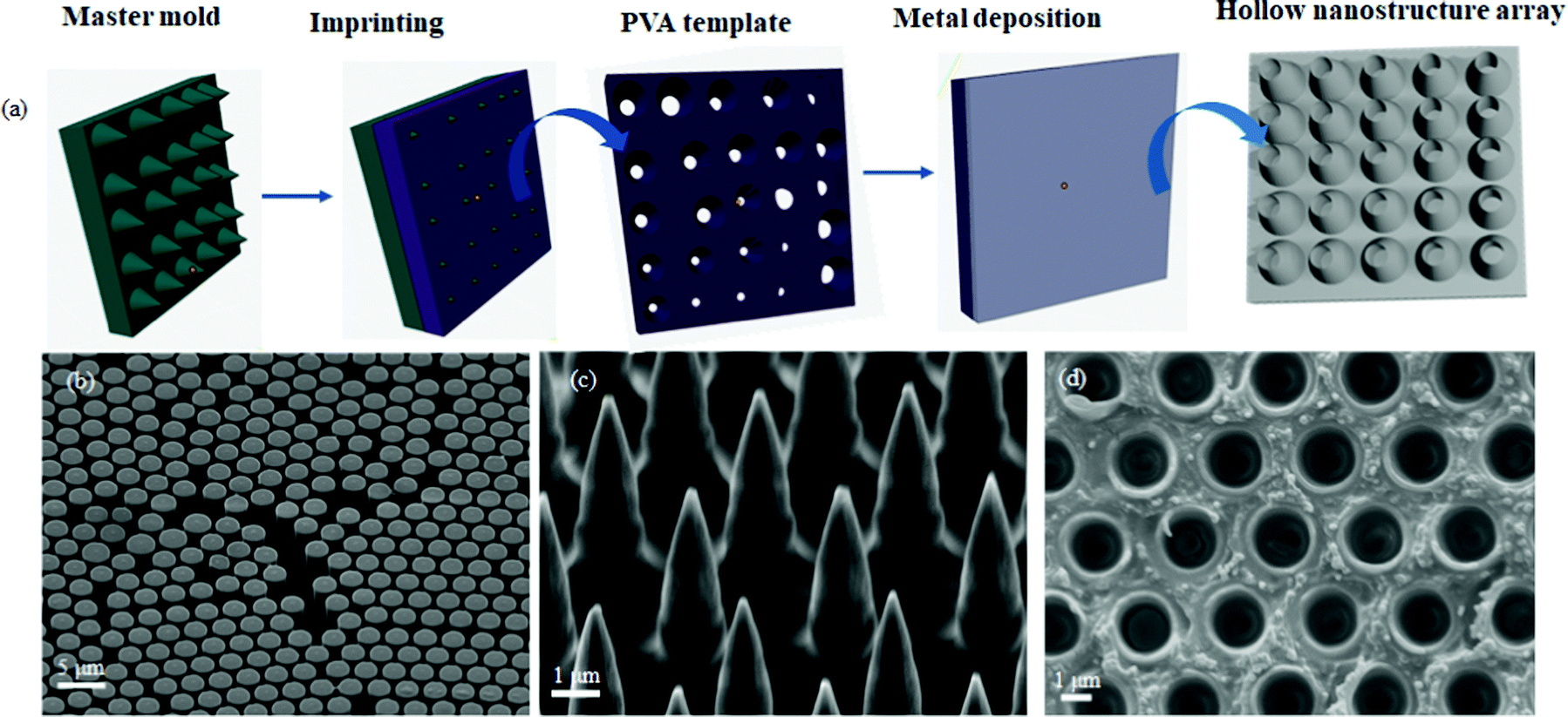 | ||
| Fig. 1 (a) Illustration of the preparation of hollow metal nanostructures. Surface morphology of (b) Si micropillars formed through the Bosch process for 24 cycles, (c) Si master mould formed after pseudo etching the Si micropillars for 3.15 min, (d) PVA template. | ||
The cone-shaped nanostructures were then used as a master mould in the preparation of polyvinyl alcohol (PVA) templates (Fig. 1d), by casting the PVA precursor onto the nanostructured surface, followed by curing at room temperature. Each Si master mould may be re-used multiple times enabling the production of many replicas of the PVA templates.
Last, metal deposition was accomplished using magnetron sputtering in the presence of the PVA template as the substrate material. Magnetron sputtering utilizes high-energy gas ions, typically argon, to knock off atoms from the surface of a target, which then condenses onto the surface of a substrate located within the reaction chamber.18,19 The technique was selected owing to its versatility, allowing the deposition of thin films from a variety of materials including metals, ceramic and polymers.20–22 The technique is also already established at an industrial scale in electronic, automotive and biomedical sectors, which will facilitate potential upscaling of this fabrication process.18,20 After the deposition, the PVA template was dissolved in hot water, leaving well-aligned and self-supporting arrays of hollow metal nanostructures (Fig. 2).
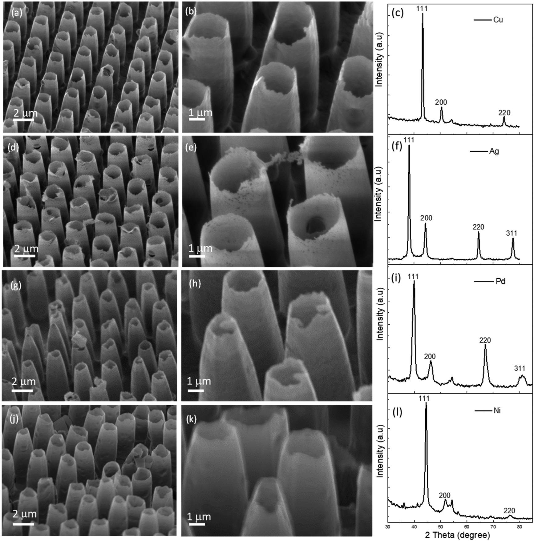 | ||
| Fig. 2 Surface morphology and X-ray diffraction (XRD) patterns of the hollow nanostructures. (a and b) Surface morphology of Cu hollow nanostructures, (c) XRD analysis of the Cu hollow nanostructures, (d and e) surface morphology of Ag hollow nanostructures, (f) XRD analysis of the Ag hollow nanostructures, (g and h) surface morphology of Pd hollow nanostructures, (i) XRD analysis of the Pd hollow nanostructures, (j and k) surface morphology of Ni hollow nanostructures, (l) XRD analysis of the Ni hollow nanostructures. | ||
As evidenced by the scanning electron microscopy images (Fig. 2), hollow nanostructures arrays could be obtained using Cu, Ag, Pd and Ni metals, demonstrating the versatility of the templated assembly technique. The height of the hollow nanostructures was typically in the range between 3.2 to 4.7 μm, while the hollow tip had diameters in the range between 1.0 to 1.5 μm, and shell thickness of less than 100 nm. The formation of the hollow nanostructures was attributed to the incomplete filling of the micro-moulds on the PVA template, which could be controlled depending on the depth of the micro-moulds. When a PVA template with much shallower micro-moulds (∼1 μm) were used, only solid nanorods were obtained without any hollow nanostructures (Fig. S2, ESI†). During the early stages of the metal deposition, metal atoms nucleated and crystalized on the surface of the PVA template (Fig. S3a, ESI†), including the inner walls of the micro-moulds across the PVA template. As the deposition progressed, the film on the top surface of the template intergrew, blocking the opening to the micro-moulds (Fig. S3b, ESI†) and therefore preventing further deposition within the voids, leading to hollow nanostructures.
Initial attempts to use polydimethylsiloxane (PDMS) template to produce such structures proved unsuccessful, as the resultant metal film could not be easily and securely detached from the PDMS without damage. PVA, on the other hand, can be easily dissolved in hot water,23 making it highly promising for the handling of such delicate nanostructures.
The crystal microstructures of the metal nanostructures were confirmed using X-ray diffraction analysis, as presented in Fig. 2c, f, i and l. The main diffraction peaks for Cu were observed at 2θ angle of 43.31°, 50.45° and 74.12°, corresponding to 111, 200, and 220 crystal planes (Fig. 2c),24 while diffraction patterns for Ag were observed at 2θ angle of 38.1° (111), 44.3° (200), 64.7° (220) and 77.5° (311).25 Diffraction peaks for Pd were observed at 2θ angle of 39.8°, 46.2°, 67° and 81.3°, corresponding to 111, 200, 220 and 311 crystal planes,26 while diffraction peaks for Ni were found at 44.4°, 51.9° and 76.2° corresponding to 111, 200 and 220 crystal planes.27 From the XRD results it is evident that the obtained nanostructures were readily crystalline, without the need for calcination. Based on the Sherrer equation,28 the Cu nanostructures were found to have an average crystallite size of 14.3 nm, while Ag, Pd and Ni had average crystal sizes of 13.7, 6.9 and 6.3 nm respectively.
Based energy dispersive X-ray analysis (EDX), the metal content was estimated to be in the range between 92 to 97 wt%, with small amounts of oxides and carbon contaminations (Fig. S4, ESI†). Cu and Ag had metal content of 94.5 and 97.3 wt% respectively, while Pd and Ni had metal content of 96 and 92.8 wt% respectively.
The potential application of the nanostructures in the electrocatalytic conversion of CO2 was investigated using copper hollow nanostructures, in the presence of 1-ethyl-3-methylimidazolium acetate ([C2mimOAc]) ionic liquid (150 mM), dissolved in dimethylacetamide (DMAc). [C2mimOAc] combined with DMAC was selected as the electrolyte owing to their higher solubilization capacity for CO2 compared to the conventional aqueous electrolytes.29–31
Fig. 3a shows the cyclic voltammetry results recorded in CO2 and N2 saturated electrolytes, with Ag/AgCl as the reference electrode and a platinum wire as the counter electrode. When the copper hollow nanostructures were used as the working electrode, the onset potential for CO2 reduction was observed at −0.04 V. This is less negative (lower overpotential) compared to that of the plain copper film, also prepared by sputtering, which had an onset potential of −0.7 V, indicating the nano-structuring improved the kinetics for the electrocatalytic reduction of CO2.32
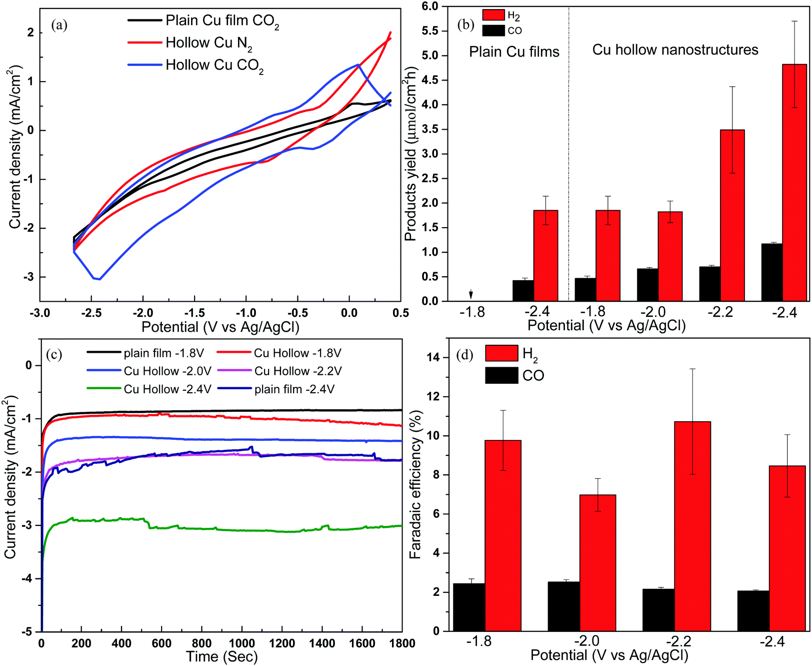 | ||
| Fig. 3 (a) Cyclic voltammetry at a scanning rate of 50 mV s−1, (b) products yield for electrocatalytic conversion of CO2 in the presence of 150 mM [C2mimOAc] dissolved in DMAC (c) current density, (d) faradaic efficiency for the Cu hollow nanostructures. | ||
Electrocatalytic studies were conducted at applied potentials between −1.8 and −2.4 V (vs. Ag/AgCl), where syngas (a mixture of H2 and CO) was found to be the only CO2 conversion products. Syngas is an important precursor in the production of various high value chemicals such as methanol, methane and diesel.33 Consistent with the cyclic voltammetry results, the hollow nanostructure exhibited a significantly higher catalytic activity as compared to the non-nanostructured plain copper film. For example, at an applied potential of −1.8 V, no detectable products were obtained when the plain Cu film was used as the working electrode (Fig. 3b). However, when the Cu hollow nanostructures were used, syngas was produced with a CO production rate of 0.46 ± 0.05 μmol cm−2 h−1 and H2 production rate of 1.85 ± 0.29 μmol cm−2 h−1. The product yield was also found to increase with the applied potential, with the CO yield increasing from 0.46 ± 0.05 to 0.7 ± 0.034 μmol cm−2 h−1 and 1.16 ± 0.034 μmol cm−2 h−1 when the potential was increased from −1.8 V to −2.2 and −2.4 V respectively, while H2 increased from 1.85 to 3.48 ± 0.9 and 4.82 ± 0.9 μmol cm−2 h−1, respectively. The increased yield at higher potential was supported by an increase in current density, which increased from 1.02 mA cm−2 to 3.04 mA cm−2 when the potential was increased from −1.8 V to −2.4 V (Fig. 3c). The CO and H2 yields at −2.4 V were 205% and 183% higher compared to that obtained with plain Cu film, which had CO yield of 0.38 ± 0.03 μmol cm−2 h−1 and H2 yield of 1.85 ± 0.29 μmol cm−2 h−1 under the same reaction conditions, highlighting the importance of the hollow nano-structuring. The enhanced performance was attributed to the higher contact surface area of the hollow nanostructure, which increases the density of active site and minimise the diffusion length for electrons.1 This was confirmed by electrochemical surface area (ECSA) measurement, using the double layer capacitance method,34,35 where Cu hollow nanostructures were found to have ECSA of 0.396 cm2, which was about 6 times higher than that of plain Cu film that had ECSA of 0.0655 cm2 (Fig. 4). No products were detected when the electrocatalytic study were conducted in N2 saturated electrolyte, with current density remaining close to zero throughout the test (Fig. S5, ESI†), confirming the generated products were indeed from the conversion of CO2. The product yields for the hollow nanostructure corresponded to faradaic efficiency of between 2–2.6% for CO generation and between 6.6% to 10.7% for H2 generation (Fig. 3d). The low current conversion efficiency for the CO formation is similar to that of other previously reported copper electrocatalysts,36,37 though the previous reports also detected other products such as CH4, C2H4, C2H6 and formate in addition to CO and H2. Although nanostructured catalysts with higher overall faradaic efficiency have been previously reported,38 most of them exhibited poor product selectivity, producing multiple mixers for gaseous and liquid products. In the current work, no other products were detected using either gas chromatography or nuclear magnetic resonance (NMR) analysis, suggesting syngas was the only product generated. Methanol and ethanol for example would have been detected at 8.3 min and 9.4 min respectively on flame ionization detector (FID) (Fig. S6a, ESI†), while C2H4, would have been detected by the thermal conductivity detector (TCD) at 2.4 min (Fig. S6b, ESI†). The product selectivity for CO2 conversion is governed not only by the catalyst properties but also by the composition of the electrolyte,39 and the electrolyte/solvent combination used in this study likely influenced the product selectivity. After exposure to the electrocatalytic reaction conditions, it was noted the copper nanostructures get oxidized when left in ambient air, with the reddish-brown colour turning to black. Future work will investigate alloyed nanostructures not only to improve the stability, but also to assess how product yield and selectivity may be modulated based on the alloy composition.40
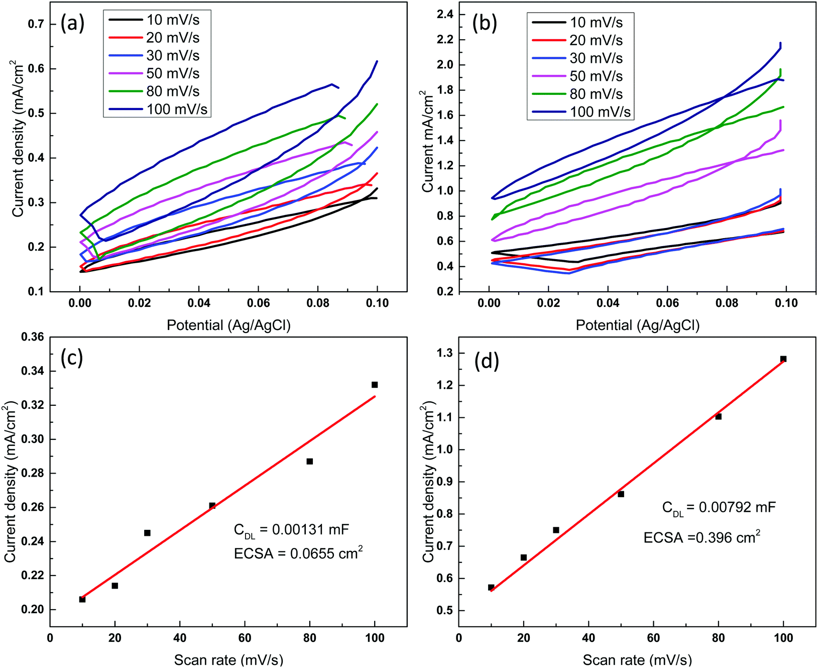 | ||
| Fig. 4 Cyclic voltammetry recorded at various scanning rate in the presence of 0.5 M KHCO3 over (a) plain copper film, (b) Cu hollow nanostructures. Plots for current vs. scan rate for (c) plain copper film, (d) copper hollow nanostructure. The slope for the plots provided double layer capacitance (CDL) values. | ||
Furthermore, although only Cu hollow nanostructures were investigated for electrocatalysis in this work, hollow metal nanostructures including Ni, Ag, and Pd have many other potential applications, owing to their ability to generate surface plasmon resonance.2 For example, it has been previously demonstrated that the surface plasmon properties for Ag nanostructures can be tuned based on the void size,2 making such nanostructures promising for a variety of applications including sensing, plasmon enhanced solar cells, Surface Enhanced Raman Spectroscopy (SERS) and photocatalysis.2,41,42
Conclusions
In summary, a templating technique for fabricating aligned and self-supporting arrays of hollow metal nanostructures was developed. The versatility of the technique was demonstrated through successful fabrication of Cu, Ag, Ni, and Pd hollow nanostructures, and the technique could potentially be extended to other metallic and metal oxide materials that can be deposited through magnetron sputtering. Hollow copper nanostructures were shown to exhibit an enhanced electrocatalytic activity of CO2 conversion to syngas, with CO and H2 production rate of more than 205% and 183% compared to that of non-nanostructured plain copper film, highlighting the potential of such nanostructures in energy conversion applications.Syngas is a valuable precursor for a variety of chemicals and fuels including methanol, methane and diesel, and the ability produce it selectively will minimize the cost incurred during the purification step. Furthermore, use of the well-established magnetron sputtering technique for the metal deposition will pave the way for potential scale-up in the future. Future work will explore the formation and application of alloyed metal hollow nanostructures, particularly how their electrocatalytic properties may be modulated depending on the alloy composition.
Conflicts of interest
There are no conflicts of interest to declare.Acknowledgements
This work was performed in part at the Melbourne Centre for Nanofabrication (MCN) in the Victorian Node of the Australian National Fabrication Facility (ANFF). Dr Maina would like to thank Deakin University for financial support through Alfred Deakin Postdoctoral Research Fellowship. The authors also acknowledge Prof. Lingxue Kong for his support and advice.References
- J. Wang, Y. Cui and D. Wang, Design of Hollow Nanostructures for Energy Storage, Conversion and Production, Adv. Mater., 2019, 31(38), 1801993 CrossRef PubMed.
- A. Genç, J. Patarroyo, J. Sancho-Parramon, N. G. Bastús, V. Puntes and J. Arbiol, Hollow metal nanostructures for enhanced plasmonics: synthesis, local plasmonic properties and applications, Nanophotonics, 2017, 6(1), 193–213 Search PubMed.
- L. Yu, X. Y. Yu and X. W. Lou, The Design and Synthesis of Hollow Micro-/Nanostructures: present and Future Trends, Adv. Mater., 2018, 30(38), 1800939 CrossRef PubMed.
- J. Park, T. Kwon, J. Kim, H. Jin, H. Y. Kim, B. Kim, S. H. Joo and K. Lee, Hollow nanoparticles as emerging electrocatalysts for renewable energy conversion reactions, Chem. Soc. Rev., 2018, 47(22), 8173–8202 RSC.
- A. G. M. da Silva, T. S. Rodrigues, S. J. Haigh and P. H. C. Camargo, Galvanic replacement reaction: recent developments for engineering metal nanostructures towards catalytic applications, Chem. Commun., 2017, 53(53), 7135–7148 RSC.
- L. F. Dumee, L. He, B. Lin, F.-M. Ailloux, J.-B. Lemoine, L. Velleman, F. She, M. C. Duke, J. D. Orbell, G. Erskine, P. D. Hodgson, S. Gray and L. Kong, The fabrication and surface functionalization of porous metal frameworks – a review, J. Mater. Chem. A, 2013, 1(48), 15185–15206 RSC.
- C. Li, M. Iqbal, J. Lin, X. Luo, B. Jiang, V. Malgras, K. C. W. Wu, J. Kim and Y. Yamauchi, Electrochemical Deposition: an Advanced Approach for Templated Synthesis of Nanoporous Metal Architectures, Acc. Chem. Res., 2018, 51(8), 1764–1773 CrossRef CAS PubMed.
- C. Li, H. Tan, J. Lin, X. Luo, S. Wang, J. You, Y.-M. Kang, Y. Bando, Y. Yamauchi and J. Kim, Emerging Pt-based electrocatalysts with highly open nanoarchitectures for boosting oxygen reduction reaction, Nano Today, 2018, 21, 91–105 CrossRef CAS.
- X. Lai, J. Li, B. A. Korgel, Z. Dong, Z. Li, F. Su, J. Du and D. Wang, General Synthesis and Gas-Sensing Properties of Multiple-Shell Metal Oxide Hollow Microspheres, Angew. Chem., Int. Ed., 2011, 50(12), 2738–2741 CrossRef CAS PubMed.
- X. Xia, Y. Wang, A. Ruditskiy and Y. Xia, 25th Anniversary Article: galvanic Replacement: a Simple and Versatile Route to Hollow Nanostructures with Tunable and Well-Controlled Properties, Adv. Mater., 2013, 25(44), 6313–6333 CrossRef CAS PubMed.
- Z. Gao, H. Ye, Q. Wang, M. J. Kim, D. Tang, Z. Xi, Z. Wei, S. Shao and X. Xia, Template Regeneration in Galvanic Replacement: a Route to Highly Diverse Hollow Nanostructures, ACS Nano, 2020, 14(1), 791–801 CrossRef CAS PubMed.
- S. Liu, X. Zheng, L. Song, W. Liu, T. Yao, Z. Sun, Y. Lin and S. Wei, Partial-surface-passivation strategy for transition-metal-based copper–gold nanocage, Chem. Commun., 2016, 52(39), 6617–6620 RSC.
- I. Mansoor, Y. Liu, U. O. Häfeli and B. Stoeber, Arrays of hollow out-of-plane microneedles made by metal electrodeposition onto solvent cast conductive polymer structures, J. Micromech. Microeng., 2013, 23(8), 085011 CrossRef CAS.
- M. W. Zhu, H. W. Li, X. L. Chen, Y. F. Tang, M. H. Lu and Y. F. Chen, Silica needle template fabrication of metal hollow microneedle arrays, J. Micromech. Microeng., 2009, 19(11), 115010 CrossRef.
- S. G. Jang, H. K. Yu, D.-G. Choi and S.-M. Yang, Controlled Fabrication of Hollow Metal Pillar Arrays Using Colloidal Masks, Chem. Mater., 2006, 18(26), 6103–6105 CrossRef CAS.
- Y. Chen, S. Aslanoglou, G. Gervinskas, H. Abdelmaksoud, N. H. Voelcker and R. Elnathan, Cellular Deformations Induced by Conical Silicon Nanowire Arrays Facilitate Gene Delivery, Small, 2019, 15(47), 1904819 CrossRef CAS PubMed.
- F. Laermer, S. Franssila, L. Sainiemi and K. Kolari, Deep reactive ion etching, in Handbook of Silicon Based MEMS Materials and Technologies, ed. M. Tilli, M. Paulasto-Krockel, M. Petzold, H. Theuss, T. Motooka and V. Lindroos, Elsevier, 3rd edn, 2020, ch. 16, pp. 417–446 Search PubMed.
- P. J. Kelly and R. D. Arnell, Magnetron sputtering: a review of recent developments and applications, Vacuum, 2000, 56(3), 159–172 CrossRef CAS.
- K. Sarakinos, J. Alami and S. Konstantinidis, High power pulsed magnetron sputtering: a review on scientific and engineering state of the art, Surf. Coat. Technol., 2010, 204(11), 1661–1684 CrossRef CAS.
- J. T. Gudmundsson, Physics and technology of magnetron sputtering discharges, Plasma Sources Sci. Technol., 2020, 29(11), 113001 CrossRef CAS.
- C. Liao, W. Wang, J. Wang, L. Han, S. Qiu, L. Song, Z. Gui, Y. Kan and Y. Hu, Magnetron sputtering deposition of silicon nitride on polyimide separator for high-temperature lithium-ion batteries, J. Energy Chem., 2021, 56, 1–10 CrossRef.
- Y. Deng, W. Chen, B. Li, C. Wang, T. Kuang and Y. Li, Physical vapor deposition technology for coated cutting tools: a review, Ceram. Int., 2020, 46(11), 18373–18390 CrossRef CAS.
- C. D. Schaper, Patterned Transfer of Metallic Thin Film Nanostructures by Water-Soluble Polymer Templates, Nano Lett., 2003, 3(9), 1305–1309 CrossRef CAS.
- A. Sahai, N. Goswami, S. D. Kaushik and S. Tripathi, Cu/Cu2O/CuO nanoparticles: novel synthesis by exploding wire technique and extensive characterization, Appl. Surf. Sci., 2016, 390, 974–983 CrossRef CAS.
- S. Saravanan, R. Kato, M. Balamurugan, S. Kaushik and T. Soga, Efficiency improvement in dye sensitized solar cells by the plasmonic effect of green synthesized silver nanoparticles, J. Sci.: Adv. Mater. Devices, 2017, 2(4), 418–424 Search PubMed.
- M. Khan, M. Khan, M. Kuniyil, S. F. Adil, A. Al-Warthan, H. Z. Alkhathlan, W. Tremel, M. N. Tahir and M. R. H. Siddiqui, Biogenic synthesis of palladium nanoparticles using Pulicaria glutinosa extract and their catalytic activity towards the Suzuki coupling reaction, Dalton Trans., 2014, 43(24), 9026–9031 RSC.
- H. Wang, X. Kou, J. Zhang and J. Li, Large scale synthesis and characterization of Ni nanoparticles by solution reduction method, Bull. Mater. Sci., 2008, 31(1), 97–100 CrossRef CAS.
- Y. Chen, X. He, X. Zhao, Q. Yuan and X. Gu, Preparation, characterization, and growth mechanism of a novel aligned nanosquare anatase in large quantities in the presence of TMAOH, J. Colloid Interface Sci., 2007, 310(1), 171–177 CrossRef CAS PubMed.
- F. Zareiekordshouli, A. Lashanizadehgan and P. Darvishi, Study on the use of an imidazolium-based acetate ionic liquid for CO2 capture from flue gas in absorber/stripper packed columns: experimental and modeling, Int. J. Greenhouse Gas Control, 2018, 70, 178–192 CrossRef CAS.
- J. W. Maina, J. A. Schütz, L. Grundy, E. Des Ligneris, Z. Yi, L. Kong, C. Pozo-Gonzalo, M. Ionescu and L. F. Dumée, Inorganic Nanoparticles/Metal Organic Framework Hybrid Membrane Reactors for Efficient Photocatalytic Conversion of CO2, ACS Appl. Mater. Interfaces, 2017, 9(40), 35010–35017 CrossRef CAS PubMed.
- J. W. Maina, C. Pozo-Gonzalo, J. A. Schütz, J. Wang and L. F. Dumée, Tuning CO2 conversion product selectivity of metal organic frameworks derived hybrid carbon photoelectrocatalytic reactors, Carbon, 2019, 148, 80–90 CrossRef CAS.
- M. He, C. Li, H. Zhang, X. Chang, J. G. Chen, W. A. Goddard, M.-J. Cheng, B. Xu and Q. Lu, Oxygen induced promotion of electrochemical reduction of CO2via co-electrolysis, Nat. Commun., 2020, 11(1), 3844 CrossRef PubMed.
- P. J. Woolcock and R. C. Brown, A review of cleaning technologies for biomass-derived syngas, Biomass Bioenergy, 2013, 52, 54–84 CrossRef CAS.
- N.-U.-A. Babar and K. S. Joya, Spray-Coated Thin-Film Ni–Oxide Nanoflakes as Single Electrocatalysts for Oxygen Evolution and Hydrogen Generation from Water Splitting, ACS Omega, 2020, 5(19), 10641–10650 CrossRef CAS PubMed.
- J. Wang, Y. Bao, C. Cui, Z. Zhang, S. Li, J. Pan, Y. Zhang, G. Tu, J. Wang and Z. Li, Fabrication of dispersive α-Co(OH)2 nanosheets on graphene nanoribbons for boosting their oxygen evolution performance, J. Mater. Sci., 2019, 54(10), 7692–7701 CrossRef CAS.
- K. D. Yang, W. R. Ko, J. H. Lee, S. J. Kim, H. Lee, M. H. Lee and K. T. Nam, Morphology-Directed Selective Production of Ethylene or Ethane from CO2 on a Cu Mesopore Electrode, Angew. Chem., Int. Ed., 2017, 56(3), 796–800 CrossRef CAS PubMed.
- C. S. Chen, A. D. Handoko, J. H. Wan, L. Ma, D. Ren and B. S. Yeo, Stable and selective electrochemical reduction of carbon dioxide to ethylene on copper mesocrystals, Catal. Sci. Technol., 2015, 5(1), 161–168 RSC.
- Z. Gu, H. Shen, L. Shang, X. Lv, L. Qian and G. Zheng, Nanostructured Copper-Based Electrocatalysts for CO2 Reduction. Small, Methods, 2018, 2(11), 1800121 Search PubMed.
- W. Zhang, Y. Hu, L. Ma, G. Zhu, Y. Wang, X. Xue, R. Chen, S. Yang and Z. Jin, Progress and Perspective of Electrocatalytic CO2 Reduction for Renewable Carbonaceous Fuels and Chemicals, Adv. Sci., 2018, 5(1), 1700275 CrossRef PubMed.
- S. Popović, M. Smiljanić, P. Jovanovič, J. Vavra, R. Buonsanti and N. Hodnik, Stability and Degradation Mechanisms of Copper-Based Catalysts for Electrochemical CO2 Reduction, Angew. Chem., Int. Ed., 2020, 59(35), 14736–14746 CrossRef PubMed.
- M. Vadai, D. K. Angell, F. Hayee, K. Sytwu and J. A. Dionne, In situ observation of plasmon-controlled photocatalytic dehydrogenation of individual palladium nanoparticles, Nat. Commun., 2018, 9(1), 4658 CrossRef PubMed.
- S. De Marchi, S. Núñez-Sánchez, G. Bodelón, J. Pérez-Juste and I. Pastoriza-Santos, Pd nanoparticles as a plasmonic material: synthesis, optical properties and applications, Nanoscale, 2020, 12(46), 23424–23443 RSC.
Footnote |
| † Electronic supplementary information (ESI) available. See DOI: 10.1039/d1ma01142a |
| This journal is © The Royal Society of Chemistry 2022 |