
 Open Access Article
 This Open Access Article is licensed under a Creative Commons Attribution-Non Commercial 3.0 Unported Licence
Role of carbon quantum dot for enhanced performance of photo-absorption in Cu2CoSnS4 superstrate solar cell device
D.
Sivagami
 *a and
B. Geetha
Priyadarshini
b
*a and
B. Geetha
Priyadarshini
b
aDepartment of Physics, Hindusthan College of Arts & Science, Coimbatore, Tamil Nadu, India. E-mail: dssivagami@gmail.com
bDepartment of Physics, Nanotech Research Innovation & Incubation Centre, PSG Institute of Advanced Studies, Peelamedu, Coimbatore, Tamil Nadu, India
First published on 25th January 2022
Abstract
In the present work, superstrate type ITO/CdS/Cu2CoSnS4 (CCTS) and Cu2CoSnS4:CQD (CCTS:CQDs)/Al thin-film solar cells are reported. An attempt was made to fabricate CCTS and CCTS:CQD thin-film absorbers using spray pyrolysis at a deposition temperature of 170 °C. In order to increase the crystallization performance, thin films were annealed at 250 °C for 30 min under N2 atmosphere using rapid thermal annealing. The XRD results showed the formation of the stannite structure for both CCTS and CCTS:CQD and the phase purity was confirmed by Raman analysis. The XPS spectra indicated oxidation states of Cu, Co, Sn, and S to be Cu+, Co2+, Sn4+, and S2− in CCTS and CCTS:CQD films. The band gap of the films was obtained as 1.35 and 1.26 eV for CCTS and CCTS:CQD. The CCTS:CQD device shows an improved efficiency (0.07%) over the CCTS device (0.003%). Impedance measurement was performed to analyze the interface between contacts and the bulk. These results showed that carbon quantum-dot-based chalcogenides can effectively absorb UV-visible photons and separate electrons and holes as potential candidates for future low-cost large-area inorganic solar cells.
1. Introduction
Solution-processed solar cell devices collect abundant solar energy to convert it into electrical energy while maintaining low manufacturing costs compared to conventional crystalline semiconductor devices.1 The size of quantum dot changes the band gap that allows an efficient absorption throughout the solar spectrum among the emergent materials for the third generation of photovoltaics.2 Solar cells based on quantum dots have attracted a lot of attention during the past few years due to the possibility of enhancing the energy conversion efficiency beyond the conventional Shockley–Queisser limit of 32% for Si-based solar cells.3 In addition, the device configuration is also important to improve the electrical performance of a device. An absorber material used in a solar cell as a superstrate configuration exhibits a better electrical behavior than the substrate configuration. In the superstrate configuration, a glass substrate performs as a support structure, as windows for illumination and as an encapsulation of the device. Superstrate-type solar cells have the merits of lower costs and easier processing than substrate solar cells and could serve as a top cell in tandem solar cells.4 Berruet et al. reported the efficiency of the CZTS superstrate type as 3.5%. They used n-type and top electrode as In2S3 and graphite.5 Yan et al. found an efficiency of 2.15% for CZTS in superstrate configuration; they incorporated a P3HT layer into a p-type layer with a Cu electrode.6 Tumbul et al. revealed the efficiency of a solar cell with superstrate type CZTS as 0.7%. They used In2S3 as buffer layer and silver paste as electrode.7 Moreover, an absorber material of a chalcogenide semiconductor offers a tunable optical band gap, high photo-absorption and a favorable band alignment, which were used in solar cell applications.8 Carbon-based materials provide an exciting opportunity in the fields of material chemistry and nanotechnology. In this scenario, carbon-based quantum dots (CQDs) have emerged as potential candidates for solar devices. In recent years, CQD materials have been widely used in dye-sensitized and organic solar cells to improve light absorption9 and promote multiple excitons,10 charge transfer11 and separation.12 The stability of organic and dye-sensitized solar cells is poor compared to that of inorganic-based chalcogenide materials. It is important to understand the interaction of such novel carbon dots with quaternary chalcogenide nanocomposites. The carbon-based materials are a very promising material for the transport of charge carriers and are not degraded with temperature. Thus, these are highly stable and flexible materials to absorb photons, having a size of a few nanometers.CQDs have a high photon absorption capability which can be utilized in organic (9.64%), dye-sensitized (10%) and perovskite (∼19%) solar cell devices.13–15 Moreover, CQD-based nanocomposites, such as chalcogenide materials, can lead to improved device performance. In this regard, Cu2CoSnS4 (CCTS) has emerged as one of the potential absorber materials for thin-film solar cells, due to direct band gap energy (1.4 eV) and high absorption coefficient (104 cm−1).16,17 A CCTS thin film can be deposited by numerous methods, such as spin coating,16 spray pyrolysis18 and RF magnetron sputtering.19 Among the different existing methods, the spray pyrolysis technique is broadly used and has several advantages, such as non-vacuum and large surface area for deposition. Maldar et al. stated that the efficiency of CCTS was 1.78% achieved at 350 °C in a photoelectrochemical method.19 The photon energy was greater than the band gap (E ≥ Eg), which means that photons have the potential to be absorbed and generate a photocurrent.20,21 Sivagami et al. reported that CQD-based CCTS can be used as a potential absorber layer for thin-film solar cells. They obtained quantum-confined carbon with CCTS nanostructures and observed a photosensitivity of ∼40% higher than that of CCTS.22 Thus, we attempted to utilize CCTS:CQD as an absorber layer for further fabrication of a superstrate solar cell and studied the performance of the device.
In the present work, a thin-film solar cell was fabricated in the superstrate configurations: ITO/CdS/CCTS/Al and ITO/CdS/CCTS:CQD/Al. CCTS and CCTS:CQD nanocomposite powders were synthesized by the direct pyrolysis method. The photosensitivity enhancement of CCTS:CQD can improve the electrical performance of the device. In this aspect, CCTS and CCTS:CQD thin films were deposited on an ITO/CdS layer by the spray pyrolysis technique. Novel CCTS:CQD-based heterostructures executed the effective separation of photogenerated electrons and holes for the solar cell.
2. Experimental work
2.1. Substrate cleaning
Before the deposition started, ITO-coated glass substrates were cleaned with a soap solution, ethanol and acetone under sonication for 5 min each. A pattern (20 mm × 5 mm) was formed on ITO substrates (10 ohm per sq.) using dilute hydrochloric acid at 55 °C for 10 min. Subsequently, the patterned substrates were cleaned with distilled water, ethanol and acetone in an ultrasonication bath for 10 min each and then dried under nitrogen flow.2.2. Device fabrication
The ITO substrates (2 × 2 cm2) were coated with a thin layer of CdS. Subsequently, the absorber layers (CCTS and CCTS:CQD) were deposited using the spray pyrolysis technique. Finally, an Al electrode was deposited on the absorber layer by the thermal evaporation method. The configurations of the devices were ITO/CdS/CCTS/Al and ITO/CdS/CCTS:CQD/Al. The process of each layer can be explained as follows.![[thin space (1/6-em)]](https://www.rsc.org/images/entities/char_2009.gif) :3 for CCTS:CQD nanocomposite. Crystallization was also confirmed at the powder stage. However, the materials mentioned were dissolved in a suitable solvent to deposit them as a thin film to observe the photosensitivity. The viscosity of the solution was adjusted by the ratio of solvent and synthesized material (v/wt%). Zhang et al. also reported that as-synthesized Cu2CoSnS4 nanocrystals were dissolved in hexane to form a colloidal ink to deposit the thin film on the substrate. No changes were observed in the crystalline structure due to the value of pH used.24 We have shown that the proposed ratio (10:3) leads to better electrical performance for solar cell application.22 The optimized ratio was used for further thin-film deposition in order to analyze the CCTS and CCTS:CQD thin films in this work.
:3 for CCTS:CQD nanocomposite. Crystallization was also confirmed at the powder stage. However, the materials mentioned were dissolved in a suitable solvent to deposit them as a thin film to observe the photosensitivity. The viscosity of the solution was adjusted by the ratio of solvent and synthesized material (v/wt%). Zhang et al. also reported that as-synthesized Cu2CoSnS4 nanocrystals were dissolved in hexane to form a colloidal ink to deposit the thin film on the substrate. No changes were observed in the crystalline structure due to the value of pH used.24 We have shown that the proposed ratio (10:3) leads to better electrical performance for solar cell application.22 The optimized ratio was used for further thin-film deposition in order to analyze the CCTS and CCTS:CQD thin films in this work.
The synthesized powders of CCTS and CCTS:CQD were dispersed in 2-methoxyethanol at 1.33 wt% for the deposition of thin films. The substrate temperature for spray pyrolysis was chosen at 170 °C for 2 min at a flow rate of 2 ml/min and a pressure of 2 bar. The ITO/CdS/CCTS and ITO/CdS/CCTS:CQD thin films were annealed by a rapid thermal annealing process (RTP) at 250 °C for 30 min under N2 atmosphere. The CdS compound was not affected at 250 °C because the ITO/CdS layer was annealed at 200 °C before the deposition of absorber layer.25 The CdS/CCTS interface was annealed at over 300 °C, as reported in the literature.26,27 Interesting properties have been reported that RTP generates for the absorbers such as: improvements in the grain size, reduction of S defects and increase in crystalline quality of films with short cycle times and low thermal budgets.26
Finally, Al electrodes were deposited by thermal evaporation on the CCTS and CCTS:CQD films using a shadow mask of dimensions 20 mm × 2 mm (length × width). Each device had a total area of approximately 0.4 cm2.
2.3. Characterization
X-Ray diffraction (XRD) patterns were recorded using CuKα radiation (k = 1.5406 Å; Empyrean, Malvern Panalytical multipurpose diffractometer, Netherlands). The Raman analysis was carried out with a confocal Raman spectrometer at an excitation wavelength of 532 nm of a He–Ne laser as an excitation source with 3 mW power. The X-ray photoelectron spectroscopy (XPS) analysis was done using a PHI 5000 VersaProbe II (ULVAC-PHI Inc., USA) equipped with micro-focused (200 μm, 15 kV) monochromatic Al-Kα X-ray source (hν = 1486.6 eV). The optical transmittance was recorded by a UV-Vis-NIR spectrophotometer (UV-Vis-1800, Shimadzu, Japan) over a wavelength range of 300–900 nm. The surface morphology, cross section of the devices and their corresponding EDS mapping were obtained using a Carl Zeiss Sigma with Gemini Column (USA) with EDAX (NanoXFlash detector, Bruker, Germany). The surface topology and roughness were observed using an atomic force microscope (NTMDT, INTEGRA Prima model, Russia). Photoluminescence (PL) measurement was carried with an RF 5000 (Shimadzu). I–V characteristics were measured using a Keysight source meter under light illumination by a solar simulator (AM 1.5, 100 mW cm−2), the measurements being carried out in air at room temperature. The impedance measurement was carried out using a Keysight E4990A (20 Hz–20 MHz) impedance analyzer and the equivalent circuits were fitted by the software EC-Lab V10.40.3. Results and discussion
3.1. Structural properties
XRD patterns of the CCTS and CCTS:CQD thin films are shown in Fig. 1(a). A strong peak was observed for the plane (112) and weak reflections for (204) and (312). The spray-deposited CCTS and CCTS:CQD thin films have a stannite structure confirmed by the standard JCPDS card no. 00-026-0513.18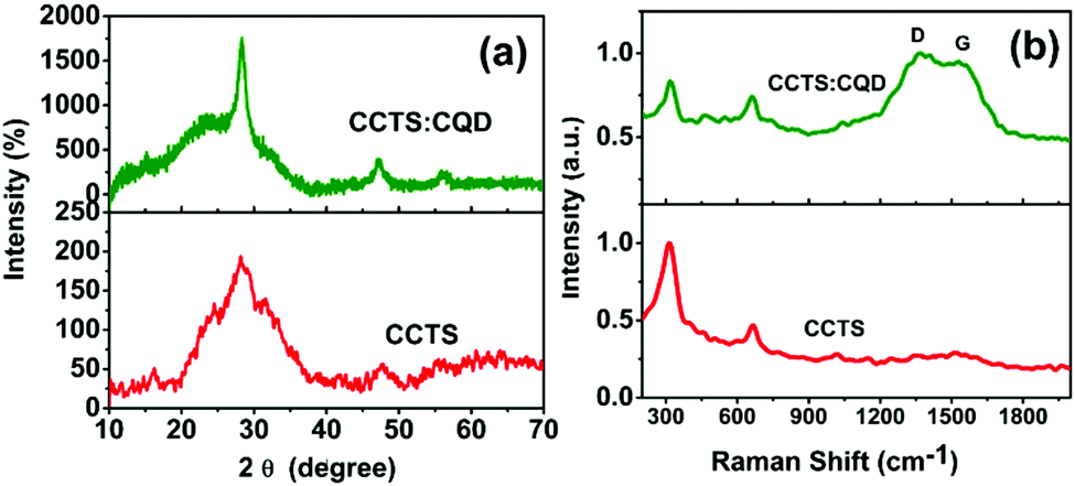 | ||
| Fig. 1 (a) XRD patterns and (b) Raman spectra of CCTS and CCTS:CQD thin films. | ||
The average crystallite size of CCTS and CCTS:CQD was obtained by Scherrer's formula as follows:
| Material | Standard diffraction angle (2θ) | Obtained diffraction angle (2θ) | FWHM (rad) | d (Å) | Crystalline size (nm) |
|---|---|---|---|---|---|
| CCTS | 28.59 | 28.12 | 0.014 | 3.17 | 10.1 |
| CCTS:CQD | 28.29 | 0.005 | 3.15 | 26.7 |
The structural parameters of CCTS and CCTS:CQD thin films for the plane (112) are shown in Table 1. The crystallite size was increased from 10.1 to 26.7 nm for CCTS and CCTS:CQD nanocomposite. Further, the phase purity of CCTS and CCTS:CQD thin films was confirmed by Raman analysis.
The peak intensity depends on the volume of diffracted matter. Intensity is proportional to the number of scatterers per unit area of a given atomic plane and therefore the peak intensities in an XRD experiment will vary. The peak intensity increases when the number of layers increases, where the thickness of the material has an important role. The crystal structure describes the atomic arrangement of a material. Interatomic distances determine the positions of the diffraction peaks. In Fig. 1(a), the relatively intense and sharp peaks were observed to become more pronounced in the presence of CQD. As the peaks in the XRD patterns intensified, the FWHM was observed to be reduced. This observation reveals the improvement of the crystallinity of the films which has been induced by CQD.28 CQD can improve not only the stability of CCTS but it also enhances the crystal quality of the CCTS:CQD thin films. For the CQD-substituted CCTS films, the intensity of the predominant peak was comparatively higher than that of the CCTS film and also FWHM of the CCTS:CQD peak was less than that of the CCTS peak, indicating improved crystalline quality of the film samples by CQD substitution. In addition, the crystalline quality of the films also depends on the nucleation and structural refinements.29,30 The halo curve of CCTS (2θ values) rises due to the sample holder.31
3.2. Raman analysis
Raman analysis was used to confirm the phase purity of thin films deposited by spray pyrolysis, as shown in Fig. 1(b). The Raman spectra of CCTS and CCTS:CQD were observed in the range of 300 to 1800 cm−1. A high-intensity CCTS peak was found at 320 cm−1, which confirms the formation of CCTS material.18 Second order peaks also appeared at 667 cm−1. In addition, the CCTS:CQD spectrum reveals the presence of CCTS material with carbon composites of D and G band values at 1391 and 1528 cm−1. The strongest peak of CCTS can be attributed to the A1 symmetry. The A1 phonon mode is a pure anion mode which corresponds to the vibration of S atoms surrounded by stationary neighboring atoms.32 Thus, the phase formation of CCTS and CCTS:CQD was confirmed by Raman analysis.3.3. XPS analysis
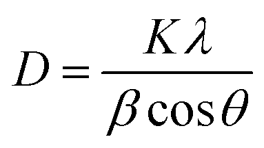
Fig. 2 shows the typical survey spectrum of CCTS thin film with corresponding valence state elements of Cu 2p region, Co 2p region, Sn 3d region and S 2p region. In addition to these elements, the presence of C from reference and O from impurity was noticed. In addition, N 1s element was present due to RTP annealing under N2 atmosphere as shown in the survey spectrum of Fig. 2(a). The Cu 2p region shows two peaks at binding energies of 932.4 eV and 952.3 eV for Cu 2p3/2 and Cu 2p1/2 with peak splitting of 19.9 eV, which was attributed to the existence of Cu1+ in CCTS as shown in Fig. 2(b).18,33–35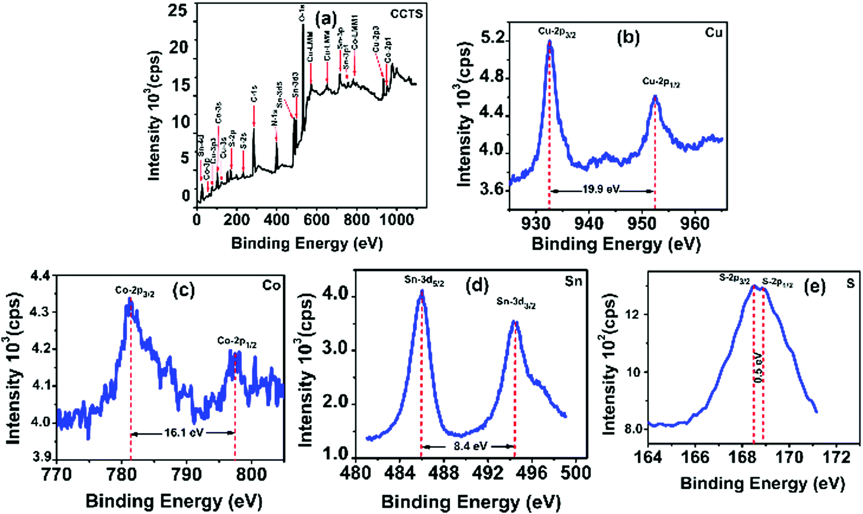 | ||
| Fig. 2 XPS analysis of CCTS thin film: (a) survey spectrum with corresponding elements of (b) Cu 2p, (c) Co 2p, (d) Sn 3d and (e) S 2p. | ||
It represents the peak splitting of 16.1 eV as shown in Fig. 2(c), which indicates the presence of Co2+.18,33–35 In Fig. 2(d), Sn 3d displays two peaks at binding energies of 486 eV and 494.4 eV for Sn 3d5/2 and Sn 3d3/2 with peak splitting of 8.4 eV, denoting the Sn4+ valence state in CCTS.18,33–35 The S 2p region depicts the two peaks of S 2p3/2 and S 2p1/2 at binding energies of 168.4 eV and 168.9 eV respectively as shown in Fig. 2(e). The difference in these peaks was calculated to be 0.5 V, which was consistent with 160 eV to 164 eV range expected for S in sulfide phases. Hence the obtained values were in good agreement with the existence of S2− in CCTS.18,33–35 From the XPS analysis of CCTS, we can conclude that valence states such as Cu (+1), Co (+2), Sn (+4), and S (−2) were present in the CCTS films.
Fig. 3 shows the typical survey spectrum of CCTS:CQD thin film with corresponding valence state elements of Cu 2p region, Co 2p region, Sn 3d region and S 2p region. The presence of C from reference and O from impurity was noticed in CCTS:CQD. In addition, N 1s element was present due to RTP annealing under N2 atmosphere as represented in Fig. 3(a). The peak splitting of Cu 2p, Co 2p, Sn 3d and S 2p was observed as 19.7 eV, 15.8 eV, 8.1 eV and 0.4 eV as displayed in Fig. 3(b–e). The elements of Cu 2p, Co 2p, Sn 3d and S 2p also exhibited the valence states of Cu (+1), Co (+2), Sn (+4), and S (−2) in the CCTS:CQD thin film. The composition of each element with impurities is presented in Fig. 3(f). Fig. 3(f) clearly shows that the carbon content was higher for CCTS:CQD than for CCTS due to the presence of CQD.
 | ||
| Fig. 3 XPS analysis of CCTS:CQD thin film: (a) survey spectrum with corresponding elements of (b) Cu 2p, (c) Co 2p, (d) Sn 3d and (e) S 2p. (f) Atomic percentages of CCTS and CCTS:CQD thin films. | ||
Also, the presence of carbon can slightly change the atomic percentage of other elements. The composition ratio was calculated for CCTS and CCTS:CQD thin films based on the values shown in Fig. 3(f). The composition ratio of CCTS was calculated to be 0.487, 0.15 and 0.69 at% for Cu/(Co + Sn), Co/Sn and S/(Cu + Co + Sn). For CCTS:CQD, the calculated values were 0.03, 0.16 and 0.2 at% for Cu/(Co + Sn), Co/Sn and S/(Cu + Co + Sn).
3.4. Optical properties
Fig. 4(a) shows the absorption spectra of CCTS and CCTS:CQD thin films, having a longer absorption wavelength range of 400 to 900 nm. CCTS:CQD shows a higher absorbance than CCTS, which reveals that more photons were absorbed by the CCTS:CQD material. The incident photons can interact with the valence electrons, and move them to the conduction band to increase the flow of electrons. The electronic transition of the films was observed via the relation of absorption coefficient and photon energy:36| αhν = A(hν − Eg)n |
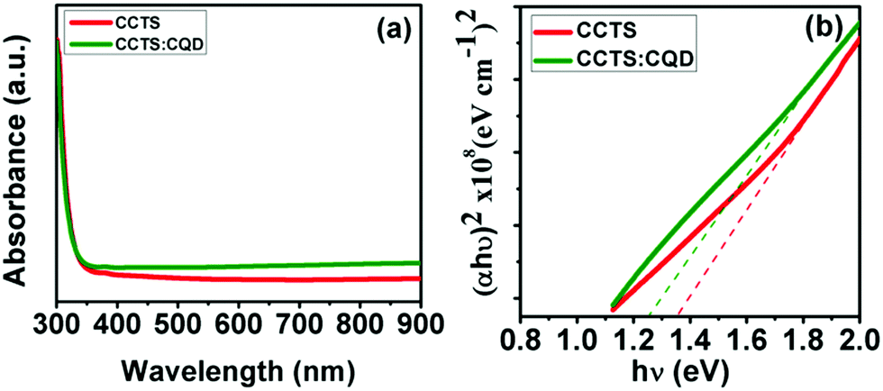 | ||
| Fig. 4 (a) Absorption spectra and (b) band gaps of CCTS and CCTS CQD thin films. | ||
The high absorption coefficient and optimum band gap of a film can allow it to act as an absorber layer for solar cells allowing efficient photon absorption and subsequent generation of electron–hole pairs. However, the absorption property might be changed with a change in the composition and morphology of the surface, which was analyzed by studies described in the following.
3.5. Morphology of CCTS and CCTS:CQD thin films with EDS mapping
Fig. 5 depicts the FESEM images and the EDS mapping of CCTS thin film. Fig. 5(a) reveals agglomerated particles in a few spots. The presence of elements was confirmed by EDS analysis (Fig. 5(b)) and mapping on a 5 μm scale was analyzed (Fig. 5(c)). The elemental mapping clearly shows the existence of all quaternary elements such as Cu, Co, Sn and S (Fig. 5(d–g)).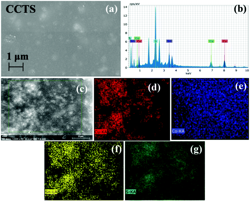 | ||
| Fig. 5 (a) FESEM image of CCTS. (b) EDS spectrum and elemental mapping of CCTS as (c) morphology at 5 μm for mapping (d) Cu, (e) Co, (f) Sn and (g) S. | ||
The EDS analysis of CCTS indicated that Cu, Co, Sn and S were present in the sample and distributed uniformly throughout the layer. Meanwhile, the corresponding average atomic percentage of Cu, Co, Sn and S was obtained as 28.12, 14.13, 26.56 and 31.19 at%. The atomic ratio of Cu:Co:Sn:S slightly deviated to 2:1:1:4. The composition variation can be represented in terms of Cu/(Co + Sn), Co/Sn and S/(Cu + Co + Sn) as 0.69, 0.53 and 0.45 for CCTS, and 1.28, 0.73 and 0.88 for CCTS:CQD films, as shown in Table 2. Specifically, the Cu, Co and Sn ratio increased and the sulfur ratio reduced due to the sulfur deficiency in RTP annealing.
| Thin film/elements | Atomic composition (%) | |||||||
|---|---|---|---|---|---|---|---|---|
| Cu | Co | Sn | S | C | Cu/(Co + Sn) | Co/Sn | S/(Cu + Co + Sn) | |
| CCTS | 28.12 | 14.13 | 26.56 | 31.19 | — | 0.69 | 0.53 | 0.45 |
| CCTS:CQD | 13.73 | 4.50 | 6.20 | 21.40 | 54.17 | 1.28 | 0.73 | 0.88 |
Fig. 6 shows the FESEM images of CCTS:CQD thin film and the elemental mapping. The high- and low-resolution images of CCTS:CQD are shown in Fig. 6(a) and its inset. The morphology reveals the presence of nanorod-like and flake-like structures found throughout the film. The nanorod structure could be formed due to the aggregation of CCTS:CQD, which creates a transformation in the structure. The nanorod structure was observed for CCTS:CQD nanocomposite, which could be because diffusion arises from the thermal behavior of clusters. The formation of nanorod structure consists of the following nucleation and aggregation steps.40 CCTS:CQD was nucleated during thermal annealing, which was aggregated in a direction rapidly. The primary CCTS:CQDs undergo a nucleation process and further growth can exhibit the rod-like structure. This structure has been formed only with the presence of C-dots, the C-dots being responsible for the formation of rod-like morphology. The rod-like CCTS:CQD was formed through the flake-cracking mechanism, the flakes were cracked in the form of nanorods during RTP and materials were transformed into rod-like morphology with the presence of carbon. Due to the size in the nanometer range, we could not determine whether the atomic center was carbon or CCTS. The FESEM images clearly show that the small grains coalesced and formed a rod-like structure.
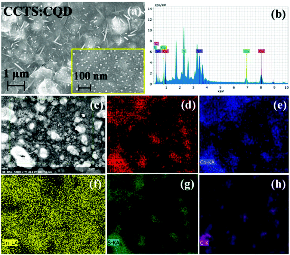 | ||
| Fig. 6 (a) FESEM images of CCTS:CQD thin film (inset at high magnification). (b) EDS spectrum. (c) Surface morphology for elemental mapping of (d) Cu, (e) Co, (f) Sn, (g) S and (h) C. | ||
When the temperature or annealing time increased, a larger nucleation and growth process could be enabled to afford an even more rod-like structure. However, the composition analysis of CCTD:CQD shows lower atomic percentages for all constituents of Cu, Co, Sn and S, although the amount of carbon (54.17 at%) was high. The EDS spectrum clearly shows the presence of Cu, Co, Sn, S and C in Fig. 6(b). The stoichiometry and crystalline quality of the absorbing material have an important influence on the performance of solar cells.41 The chemical composition of the deposited thin film depends on that of the coating solution. The ratios of Cu/(Co + Sn) and Co/Zn were decreased from 1.28 to 0.73 in the starting material. Yeh reported that defect clusters should be avoided to maintain the Cu/(Zn + Sn) atomic content ratio at less than 1, the Zn/Sn atomic content ratio should be more than 1, and the S/(Cu + Zn + Sn) in CZTS thin films can approach 1.41 This shows Cu-rich and Co-poor composition, which creates antisite defects such as CuCo and SnCo. However, the constituent elements were distributed uniformly. The shortage of quaternary constituent elements can lead to the poor performance of solar cell devices. Cu-poor kesterites show less Cu/Zn disorder than Cu-rich kesterite.42
The variation in composition ratio leads to antisite defects in CZTS and reduced efficiency of a device.43–45 The excess amount of carbon (confirmed by mapping) could be aggregated with the quaternary material. The nucleation and aggregation of carbon dot formed a rod-like structure.
The composition variation of CCTS (Cu: 28.12, Co: 14.13, Sn: 26.56 and S: 31.19%) and CCTS:CQD (Cu: 13.73, Co: 4.50, Sn: 6.20 and S: 21.40%) thin films was observed, which could be because of the different evaporation rates for different metal precursors. In contrast, the stoichiometric ratio for both CCTS and CCTS:CQD thin films was close to 2:1:1:4. Indeed, additional peaks were not observed in XRD and Raman analyses, which supports the formation of single-phase CCTS and CCTS:CQD. The sharp XRD peak of the nanocomposite indicates that the CCTS:CQD nanorods were almost aligned and the direction of growth was nearly perpendicular to the base surface. The variation of the chemical composition had no influence on the XRD pattern of the material, which could not lead to secondary phases or other prominent peaks.43 The possibility of reduced amounts of Co and Sn was considered to be due to evaporation, since the CCTS thin films contained no secondary phase.44 In XRD, the crystallite size of CCTS:CQD (26.7 nm) was higher than that of CCTS (10.1 nm) due to the increase in the Cu/(Co + Sn) ratio, indicating an improvement in grain growth under Cu-rich condition.45 Chen et al. reported that the composition (mixed cations) retained the pure kesterite structured CZTS and CZTSSe.46 Shyju et al. obtained the structure of single-phase CZTS kesterite even if the stoichiometric ratio deviated.47 According to the first principle calculation, kesterite CZTS (Cu-poor, Zn-rich) creates defect clusters such as [Vcu + ZnCu], [ZnSn + 2ZnCu] and [2CuZn + SnZn].48 These intrinsic defects act as shallow acceptors and show p-type conductivity. The distribution of the elements in CCTS:CQD was observed by elemental mapping for the area of 5 μm as shown in Fig. 6(c–h), suggesting that elements were evenly distributed.
Fig. 7(a and b) shows the cross-sectional FESEM images and related EDS elemental mapping of a device (ITO/CdS/CCTS:CQD/Al). The elemental mapping clearly shows the distribution of the elements present in ITO, CdS and CCTS:CQD and Al, as presented in Fig. 7(c–i). The individual layers were clearly observed. In the absorber layer the elements Cu, Co, Sn, and S were distributed uniformly. The uniform distribution of elements promoted the adhesion of the final CCTS:CQD layer on the CdS/ITO substrate.
 | ||
| Fig. 7 (a) Cross-sectional FESEM image of ITO/CdS/CCTS:CQD/Al device. (b) Cross section in 5 μm scale for elemental mapping. The elemental distributions of (c) Cu, (d) Co, (e) Sn, (f) S, (g) Cd, (h) In and (i) Al. | ||
Additionally, there was no clear boundary of ITO and Al contacts, indicating the inter-diffusion of In and Al across the p- and n-type layer observed from mapping of Fig. 7(h and i). The reason could be the thermodynamically unstable feature of ITO back contact and the subsequent layers.49,50 The thickness of CdS, CCTS and CCTS:CQD was measured after annealing by RTP. The thickness of CdS and CCTS:CQD was observed from the FESEM analysis, as shown in Table 3.
| Device name | Configuration | Thickness (nm) |
|---|---|---|
| Device 1 | Glass/ITO/CdS/CCTS/Al | CdS: 50 CCTS: 320 |
| Device 2 | Glass/ITO/CdS/CCTS:CQD/Al | CdS: 50 CCTS:CQD: 370 |
3.6. Surface topography of CCTS and CCTS:CQD
The surface topography of CCTS and CCTS:CQD was shown in Fig. 8(a and b). CCTS has a large grain size of ∼13.2 nm compared to CCTS:CQD at ∼19.8 nm. The agglomeration of CCTS:CQDs was observed in Fig. 8(b). These grain sizes were larger than the crystallite sizes of these samples obtained from the XRD patterns, due to agglomeration of many nanocrystallites forming the grains.51 The composite material shows a reduction in size compared with CCTS, which leads to improvement in electron transfer. However, the grains were stretched in one direction (rod-shaped), which was corroborated by the SEM morphology. The rod-like structure provides a direct path for photogenerated electrons that could reduce electron recombination on the grain boundaries, which might promote the efficiency of current nanocrystal-based solar cells.52 It is plausible that carbon-containing ligands in CZTS limit the grain growth by acting as barriers between neighboring nanocrystals. Therefore, CZTS reveals abnormal grain growth at high carbon concentrations (>35 at%) (some grains grow faster than others).53 Based on this, the presence of CQD could limit the grain growth of CCTS and lead to a rod-like shape. The root mean square roughness value of CCTS and CCTS:CQD thin films was measured as 4.8 nm and 2.1 nm. These values show that the surface was quite smooth. The rough absorber layer implies a larger interface with the n-type semiconductor. The enlarged area can lead to increased recombination at the interface between the n-type and the absorber layer, the carrier collection between the absorber layer and Al contact being limited, as a result of which the overall performance of the device was reduced.54 Thus, the smooth surface (less than ∼100 nm) enables good physical contact with the resulting layer and limits the Voc and FF of the cell.55 The grains were evenly distributed over the surface of the samples.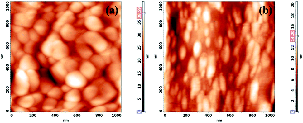 | ||
| Fig. 8 AFM 2D images of (a) CCTS and (b) CCTS:CQD thin films. | ||
3.7. PL analysis
PL spectra of CCTS and CCTS:CQD are shown in Fig. 9. PL emission of CCTS exhibits one broad asymmetric band which was peaked at 1.39 eV, which was considerably lower than the band gap energy value calculated from UV spectra. Similar asymmetric broad band and lower energy values were observed for CZTS as previously reported56–58 and has been attributed to conduction band to acceptor transitions and related recombination paths in CCTS.57,58 The intensity of CCTS emission was decreased and shifted to the red region. In addition, the PL spectrum response was relatively broad for CCTS:CQD, which could arise from the inhomogeneous size of CCTS:CQD. Notably, CCTS:CQD shows an increased emission intensity compared to CCTS due to the photoinduced electron transfer from CCTS to CQD in CCTS:CQD, which provides a non-radiative decay path. Earlier reports have demonstrated that carbon-based materials can act as good electron acceptors, and charge transfer has been enhanced in carbon-based composite systems.59,60 Electron transfer from CCTS to CQD was therefore energetically favorable when CCTS was coupled to CQD. Owing to the competition between electron transfer mechanism and electron–hole recombination, as shown in Fig. 9(b), the photoexcited electrons could be partially transferred into CQD that can carry electrons without any emission, while the remainder of electrons provides for a reduced emission by the electron–hole recombination process. However, all the photoexcited electrons were provided for reduced emission by the electron–hole recombination process in CCTS.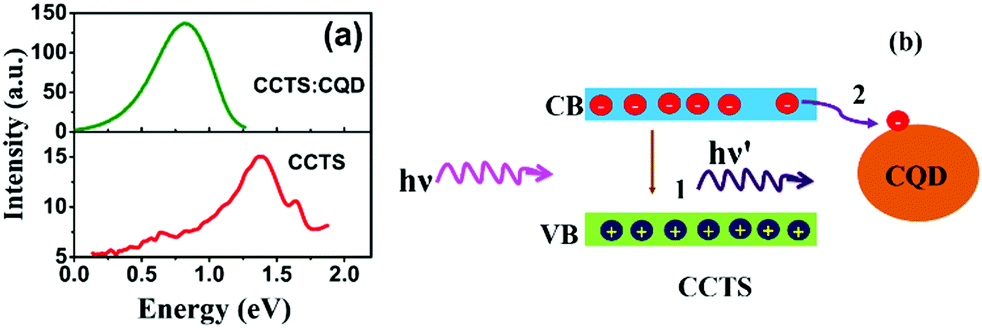 | ||
| Fig. 9 (a) Room-temperature PL spectra of CCTS and CCTS:CQD. (b) Schematic band diagram of CCTS:CQD (‘1’ represents electron–hole recombination process and ‘2’ represents photoinduced electron transfer process). | ||
3.8. Solar cell performance
A schematic diagram of the CCTS solar cell structure and the energy levels of the superstrate type are shown in Fig. 10(a and b). The n-type layer (CdS) was deposited on an ITO substrate, and then the heterojunction was formed by depositing an absorber layer followed by Al deposition. The thickness of the layers is shown in Table 3. Under light illumination, electron–hole pairs generated in the depletion region were separated by the built-in electric field with electrons drifting to the CdS layer and holes drifting to the CCTS layer. When the device terminals are shorted, excess electrons in CdS flow through the external circuit to recombine with the excess holes on the CCTS side. The electron transfer between CCTS and CQD within the CCTS:CQD nanocomposite was explained in our previous work.22 Current density–voltage (J–V) curves of the CCTS and CCTS:CQD solar cells are shown in Fig. 10(c and d). The efficiency of the solar cells was calculated for the fabricated devices, presented in Table 4.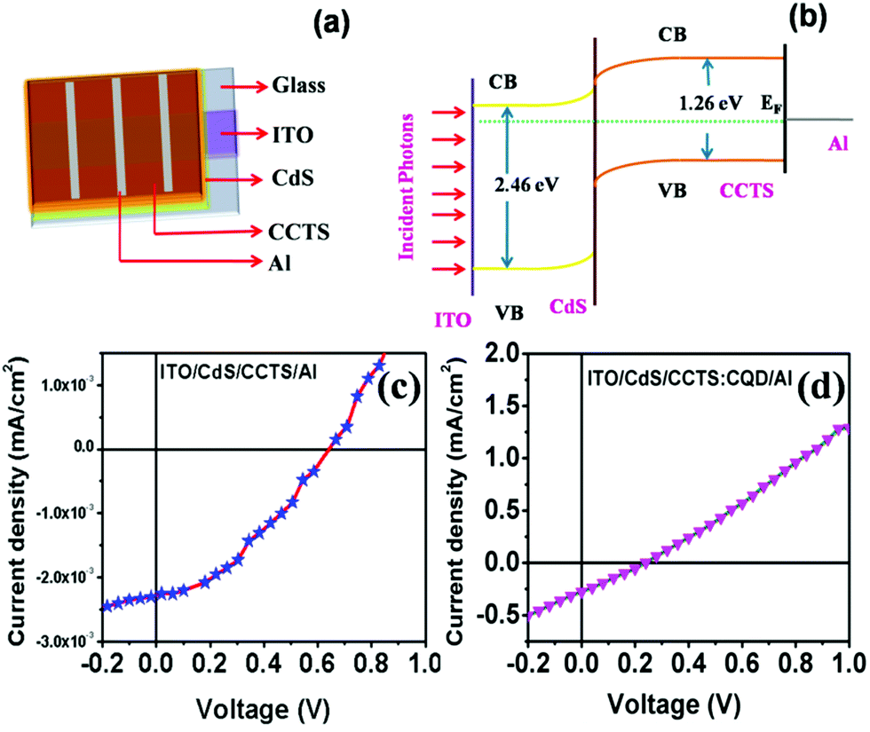 | ||
| Fig. 10 (a) Scheme for superstrate-type solar cell device. (b) Energy level diagram. J–V curves for (c) CCTS and (d) CCTS:CQD solar cell devices. | ||
| Device structure | Deposition method | J sc (mA cm−2) | V oc (V) | FF | η (%) | Active area (cm2) | Ref. |
|---|---|---|---|---|---|---|---|
| ITO/CdS/CCTS/Al | Spray pyrolysis | 0.010 | 0.70 | 36 | 0.003 | 0.4 | Present work |
| ITO/CdS/CCTS:CQD/Al | Spray pyrolysis | 1.1 | 0.24 | 26 | 0.07 | 0.4 | Present work |
| FTO/CdS/CZTS/C | Spray pyrolysis | 0.46 | 0.38 | 24 | 0.15 | 0.12 | 40 |
| FTO/TiO2/In2S3/CZTS/C | Screen printing | 8.76 | 0.25 | 27 | 0.6 | 0.25 | 41 |
| Carbon paste/CZTS/TiO2 NP/TiO2 NP/TCO | Spray pyrolysis | 2.85 | 0.56 | 43 | 0.51 | — | 42 |
| Mo/CZTS/In2S3/TiO2NP/FTO | Doctor blading | 7.82 | 0.24 | 29 | 0.55 | 1 | 43 |
The fill factor and power conversion efficiency were calculated by the following equations:
where VOC is the open circuit voltage, JSC is the short circuit current density, Vmax is maximum voltage, Jmax is maximum current density, FF is fill factor, and Pin is input power density of illuminating light.
The electrical parameters of the solar cell showed an open circuit voltage of 0.24 V, short-circuit current density of 1.1 mA cm−2, a fill factor of 26% and a conversion efficiency of 0.07%, which was lower than that of superstrate-type CZTS solar cells.61 To the best of our knowledge, the superstrate type of CCTS solar cell has not yet been reported. Therefore, Table 4 shows a comparison of the photovoltaic performances with other reported CZTS superstrate solar cells. Reports on the type of superstrate show that the efficiency can be reduced due to the band alignment between the layers of solar cells.7
It has been observed that the low efficiency of the devices was due to the inter-diffusion of elements in the cross-sectional elemental mapping of FESEM. The complexity of the morphology has a detrimental effect on the electron/hole collection. Therefore, the performance of the solar cell was dictated by balancing the influence of the morphology of the active layer on the dissociation of excitons and the charge transport.62,63 Kowalczewski et al. reported that with increasing thickness of the absorber layer (μm to 102 μm), the current density of the cell increases (16 to 35 mA cm−2).64 A higher crystallite size in the absorber is preferred in p–n junction solar cells to avoid recombination of charge carriers at grain boundaries.65 A larger size was found for CCTS:CQD than CCTS, improving the efficiency of the cell by reducing grain boundary effects.66 The thickness of the absorber layer plays an important role in determining the solar cell efficiency. The thickness of the absorber layer influences the diffusion length of the carriers. If the absorber layer was very thin, the absorption decreases, and ultimately the efficiency decreases. On the other hand, if the absorber layer was very thick, the charge carriers can recombine before they migrate to the charge collecting layers, and the efficiency decreases. The optimization of the absorber layer thickness was therefore very important in order to achieve good efficiency.
Bag et al.67 reported that the short circuit current density (JSC) increases with thickness due to improved light absorption. It increases rapidly from ∼17.76 mA cm−2 to ∼24.59 mA cm−2 for a change in thickness of 100 nm to 500 nm and furthermore increases at a decreasing rate until all light was absorbed and then to ∼25 mA cm−2 at saturation. At 100–200 nm, JSC was very low due to the lower absorption and the use of thicker (>700 nm) films was of no advantage. An absorber thickness of 600–700 nm was therefore suitable. The fill factor decreases with thickness due to an increase in the series resistance across the cell.67 With a change in thickness from 100 nm to 1000 nm, the fill factor constantly decreases from 83% to 67%.68 The decrease in the fill factor value with the increase in thickness was due to the build-up of internal power depletion, which leads to a decrease in the fill factor. VOC increases with increasing thickness due to low electron–hole recombination and high generation rate. If we increase the thickness further (>1000 nm), the rate of recombination compensates for the rate of generation and VOC remains the same. On the other hand, a larger increase in thickness leads to a decrease in VOC due to a high recombination rate and a low generation rate.68
Maximum light absorption occurs when the thickness (∼1 μm) of the absorber layer is sufficient for superstrate-type solar cells.69–72 The reason might be that a long lifetime of the carriers is provided by a thicker absorber.73,74 The CdS/CCTS interface shows a lower efficiency of 0.003%, which might be because of more defects on the interface between n- and p-type layer analyzed by impedance measurements.
3.9. Impedance spectroscopy analysis
Electrochemical impedance spectroscopy was employed to evaluate the resistance for charge carrier transfer between CdS and CCTS and CCTS:CQD thin films. The frequency-dependent impedance measurements of the CCTS- and CCTS:CQD-based solar cell devices were carried out at room temperature. In general, the impedance data are indicated in the complex-plane impedance, termed a Nyquist plot. The Nyquist plots for CCTS- and CCTS:CQD-based devices are shown in Fig. 11 and the inset shows the equivalent circuit used to obtain the probable resistive and capacitive components for the solar cells. The equivalent circuit represents that R1 = Rct and C1 = Cdl, where Rct is the charge transfer resistance and Cdl is the double layer resistance.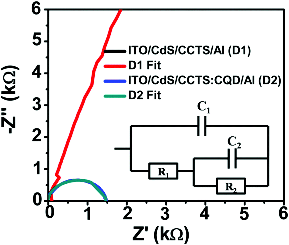 | ||
| Fig. 11 Nyquist plots of the impedance data of the CCTS and CCTS:CQD heterojunction films in the dark. | ||
The equivalent AC circuit of a p–n heterojunction solar cell consists of three elements: the series resistance (Rs) as R1 occurring due to bulk and contact resistances, the parallel resistance Rp due to recombination in the depletion region and the total capacitances (due to diffusion and depletion capacitances).75,76 The parameters obtained by fitting the experimental data to the equivalent circuit are presented in Table 5. The series resistance of R1 was obtained for CdS/CCTS and CdS/CCTS:CQD interfaces as 2523 and 508.879 Ω. The lowest charge-transfer resistance (Rct) indicates that it improves charge transfer in the CdS/CCTS:CQD layers. The parallel resistance of R2 was lower for the CdS/CCTS:CQD interface at 559.37 Ω than for the CdS/CCTS interface, which represents the reduction in the recombination rate. The semicircular nature of these Nyquist plots corroborates the control of space charge region in the ITO/CdS/CCTS:CQD/Al solar cell device. The CdS/CCTS interface not exhibiting such behavior could be because of an interface between the layers of n–p type, which confirms the presence of a dominant single space charge region in the heterojunction.40 The two capacitive values (0.0737 × 10⁻⁹ and 0.7507 × 10⁻⁹) signify that the charge transfer was limited at the interface of CdS/CCTS or CCTS:CQD and the subsequent contact of CCTS or CCTS:CQD/Al.
| Device | C 1 (F) | R 1 (Ω) | C 2 (F) | R 2 (Ω) |
|---|---|---|---|---|
| Device 1 | 0.0737 × 10⁻⁹ | 2523 | 0.2192 × 10⁻⁹ | 1584 |
| Device 2 | 0.7507 × 10⁻⁹ | 508.879 | 0.3672 × 10⁻⁹ | 559 |
A lower resistance was obtained for higher efficiency of the devices. CQD incorporation with chalcogenide was found to reduce the band gap of CCTS:CQD nanocomposite (1.26 eV), which consequently results in an improved generation of photocurrent by light absorption. This photogeneration was limited by the CdS/CCTS:CQD interface and the largest diameter of the semicircle indicates the highest value of the charge recombination resistance compared to the literature.77 However, the incorporation of CQD leads to the probable generation and separation of electrons and holes in the fabricated device.
4. Conclusion
In this study, superstrate type of CCTS and CCTS:CQD nanocomposite thin-film solar cells were fabricated. The superstrate configuration of ITO/CdS/CCTS:CQD showed a conversion efficiency of 0.07% when fabricated by the spray pyrolysis technique. To the best of our knowledge, this type of superstrate configuration was studied for the first time, especially with the incorporation of CQD improving device performance. Structural and optical studies were carried out for thin films of CCTS and CCTS:CQD. The phase purity was identified by the Raman spectra, which reveal peaks at 320 and 667 cm−1 (second-order peak). Moreover, the CCTS:CQD spectrum depicts the presence of CCTS peaks with carbon composites of D and G band values at 1391 and 1528 cm−1. The oxidation states (Cu+, Co2+, Sn4+, and S2−) of constituent elements of CCTS and CCTS:CQD films were confirmed using XPS analysis. The surface morphology of CCTS was observed as a grain-like structure. However, the CCTS:CQD nanocomposite reveals a rod-like structure due to the nucleation and growth process of grains in CCTS:CQD. The rod-like structure of CCTS:CQD could enhance the electron transport properties to afford better efficiency than CCTS. The composition of CCTS and CCTS:CQD deviates slightly from the stoichiometric ratio of 2:1:1:4 (Cu:Co:Sn:S). Concerning the chemical composition of CCTS and CCTS:CQD films, the performance of the present solar cell can be improved by optimizing it to achieve the stoichiometric ratio reported in the literature for CZTS. In addition, by changing the concentration of the precursor solution, the chemical composition of the thin film was adjusted in the present spray pyrolysis technique. Therefore, optimizing such compositional properties can improve the conversion efficiency of the solar cell with a variety of modifications involved in the structure of the device.
Author contributions
The manuscript was written through contributions from all authors. All authors have given approval to the final version of the manuscript.Conflicts of interest
There are no conflicts to declare.Acknowledgements
The author D. Sivagami acknowledges Hindusthan College of Arts and Science for encouragement to publish this work. Also, the authors acknowledge PSG Institute of Advanced Studies for providing the facilities to carry out the research on thin-film solar cells.References
- L. Tsakalakos, J. Balch, J. Fronheiser, B. A. Korevaar, O. Sulima and J. Rand, Appl. Phys. Lett., 2007, 91, 233117 CrossRef.
- I. Robel, V. Subramanian, M. Kuno and P. V. Kamat, J. Am. Chem. Soc., 2006, 128, 2385 CrossRef CAS PubMed.
- W. Shockley and H. J. Queisser, J. Appl. Phys., 1961, 32, 510 CrossRef CAS.
- F. J. Haug, H. Zogg and A. N. Tiwari, in Conference Record of the Twenty-Ninth IEEE Photovoltaic Specialists Conference, 2002, 728.
- M. Berruet, Y. Di Iorio, C. J. Pereyra, R. E. Marotti and M. Vazquez, Phys. Status Solidi RRL, 2017, 11, 1700144 CrossRef.
- R. Yan, L. Kang, Y. Sun and J. Zhang, RSC Adv., 2018, 8, 11469 RSC.
- A. Tumbul, F. Aslan, A. Göktaş and I. H. Mutlu, J. Alloys Compd., 2019, 781, 280 CrossRef CAS.
- J. Albero, J. N. Clifford and E. Palomares, Coord. Chem. Rev., 2014, 263, 53 CrossRef.
- K. H. Ye, Z. Wang, J. Gu, S. Xiao, Y. Yuan, Y. Zhu, Y. Zhang, W. Mai and S. Yang, Energy Environ. Sci., 2017, 10, 772 RSC.
- A. J. Nozik, Chem. Phys. Lett., 2008, 457, 3 CrossRef CAS.
- Q. Zhang, G. Zhang, X. Sun, K. Yin and H. Li, Nanomater, 2017, 7, 130 CrossRef PubMed.
- N. Gao, L. Huang, T. Li, J. Song, H. Hu, Y. Liu and S. Ramakrishna, J. Appl. Polym., 2020, 137, 48443 CrossRef CAS.
- R. Zhang, M. Zhao, Z. Wang, Z. Wang, B. Zhao, Y. Miao, Y. Zhou, H. Wang, Y. Hao, G. Chen and F. Zhu, ACS Appl. Mater. Interfaces, 2018, 10, 4895 CrossRef CAS PubMed.
- R. Riaz, M. Ali, T. Maiyalagan, A. S. Anjum, S. Lee, M. J. Ko and S. H. Jeong, Appl. Surf. Sci., 2019, 483, 425 CrossRef CAS.
- H. Li, W. Shi, W. Huang, E. P. Yao, J. Han, Z. Chen, S. Liu, Y. Shen, M. Wang and Y. Yang, Nano Lett., 2017, 17, 2328 CrossRef CAS PubMed.
- B. Murali and S. B. Krupanidhi, J. Appl. Phys., 2013, 114, 144312 CrossRef.
- A. Gillorin, A. Balocchi, X. Marie, P. Dufour and J. Y. Chane-Ching, J. Mater. Chem., 2011, 21, 5615 RSC.
- P. S. Maldar, M. A. Gaikwad, A. A. Mane, S. S. Nikam, S. P. Desai, S. D. Giri, A. Sarkar and A. V. Moholkar, Sol. Energy, 2017, 158, 89 CrossRef CAS.
- T. Wang, Q. Zhan and W. Cheng, J. Mater. Sci.: Mater. Electron., 2019, 30, 2285 CrossRef CAS.
- J. Day, S. Senthilarasu and T. K. Mallick, Renewable Energy, 2019, 132, 186 CrossRef.
- W. S. Choi, M. F. Chisholm, D. J. Singh, T. Choi, G. E. Jellison Jr and H. N. Lee, Nat. Commun., 2012, 3, 689 CrossRef PubMed.
- D. Sivagami, S. Thangamani, K. Mohanta, K. Mohanapriya and B. Geetha Priyadarshini, Nanotechnology, 2020, 31, 235401 CrossRef PubMed.
- D. Sivagami and G. B. Priyadarshini, Adv. Sci., 2019, 11, 571 CAS.
- X. Zhang, N. Bao, B. Lin and A. Gupta, Nanotechnology, 2013, 24, 105706 CrossRef PubMed.
- J. Kim, H. Hiroi, T. K. Todorov, O. Gunawan, M. Kuwahara, T. Gokmen, D. Nair, M. Hopstaken, B. Shin, Y. S. Lee and W. Wang, Adv. Mater., 2014, 26, 7427 CrossRef CAS PubMed.
- M. A. Olgar, J. Klaer, R. Mainz, L. Ozyuzer and T. Unold, Thin Solid Films, 2017, 628, 1 CrossRef CAS.
- M. G. Sousa, A. F. Da Cunha, J. P. Teixeira, J. P. Leitão, G. Otero-Irurueta and M. K. Singh, Sol. Energy Mater. Sol. Cells, 2017, 170, 287 CrossRef CAS.
- B. Unveroglu and G. Zangari, J. Electrochem. Soc., 2019, 166, H3040 CrossRef CAS.
- A. Goktas, A. Tumbul, Z. Aba, A. Kilic and F. Aslan, Opt. Mater., 2020, 107, 110073 CrossRef CAS.
- A. Tumbul, F. Aslan, A. Göktas, M. Z. Zarbali and A. Kiliç, Mater. Chem. Phys., 2021, 258, 123997 CrossRef CAS.
- H. Gencer, M. Gunes, A. Goktas, Y. Babur, H. I. Mutlu and S. Atalay, J. Alloys Compd., 2008, 465, 20–23 CrossRef CAS.
- H. Neumann, Helv. Phys. Acta, 1985, 58, 337 CAS.
- Y. Xie, C. Zhang, G. Yang, J. Yang, X. Zhou and J. Ma, J. Alloys Compd., 2016, 696, 938 CrossRef.
- X. Miao, R. Chen and W. Cheng, Mater. Lett., 2017, 193, 183 CrossRef CAS.
- W. Wang, H. Shen, H. Yao and J. Li, Mater. Lett., 2014, 125, 183 CrossRef CAS.
- Amorphous and liquid semiconductors, ed. J. Tauc, Springer Science & Business Media, Springer, Boston, MA, 1974, p. 159 Search PubMed.
- P. S. Maldar, A. A. Mane, S. S. Nikam, S. D. Giri, A. Sarkar and A. V. Moholkar, J. Mater. Sci.: Mater. Electron., 2017, 28, 18891 CrossRef CAS.
- R. Kumar, N. Khare, V. Kumar and G. L. Bhalla, Appl. Surf. Sci., 2008, 254, 6509 CrossRef CAS.
- M. Khammar, F. Ynineb, S. Guitouni, Y. Bouznit and N. Attaf, Appl. Phys. A: Mater. Sci. Process., 2020, 126, 1 CrossRef.
- L. S. Zhong, J. S. Hu, H. P. Liang, A. M. Cao, W. G. Song and L. J. Wan, Adv. Mater., 2006, 18, 2426 CrossRef CAS.
- M. Y. Yeh, P. H. Lei, S. H. Lin and C. D. Yang, Materials, 2016, 9, 526 CrossRef PubMed.
- S. Schorr, G. Gurieva, M. Guc, M. Dimitrievska, A. Pérez-Rodríguez, V. Izquierdo-Roca, C. S. Schnohr, J. Kim, W. Jo and J. M. Merino, J. Phys. Energy, 2019, 2, 012002 CrossRef.
- K. Tanaka, Y. Fukui, N. Moritake and H. Uchiki, Sol. Energy Mater. Sol. Cells, 2011, 95, 838 CrossRef CAS.
- S. Chen, X. G. Gong, A. Walsh and S. H. Wei, Appl. Phys. Lett., 2010, 96, 021902 CrossRef.
- A. V. Moholkar, S. S. Shinde, G. L. Agawane, S. H. Jo, K. Y. Rajpure, P. S. Patil, C. H. Bhosale and J. H. Kim, J. Alloys Compd., 2012, 544, 145 CrossRef CAS.
- S. Chen, A. Walsh, J. H. Yang, X. G. Gong, L. Sun, P. X. Yang, J. H. Chu and S. H. Wei, Phys. Rev. B: Condens. Matter Mater. Phys., 2011, 83, 125201 CrossRef.
- T. S. Shyju, S. Anandhi, R. Suriakarthick, R. Gopalakrishnan and P. Kuppusami, J. Solid State Chem., 2015, 227, 165 CrossRef CAS.
- S. Chen, A. Walsh, X. G. Gong and S. H. Wei, Adv. Mater., 2013, 25, 1522 CrossRef CAS PubMed.
- J. Ge, J. Chu, J. Jiang, Y. Yan and P. Yang, ACS Sustainable Chem. Eng., 2015, 3, 3043 CrossRef CAS.
- C. Platzer-Bjorkman, N. Barreau, M. Bär, L. Choubrac, L. Grenet, J. Heo, T. Kubart, A. Mittiga, Y. Sanchez, J. Scragg and S. Sinha, J. Phys. Energy, 2019, 1, 044005 CrossRef.
- M. Z. Ansari and N. Khare, Mater. Sci. Semicond. Process., 2017, 63, 220 CrossRef CAS.
- X. Lu, Z. Zhuang, Q. Peng and Y. Li, CrystEngComm, 2011, 13, 4039 RSC.
- B. A. Williams, M. A. Smeaton, N. D. Trejo, L. F. Francis and E. S. Aydil, Chem. Mater., 2017, 29, 1676 CrossRef CAS.
- D. Colombara, A. Crossay, L. Vauche, S. Jaime, M. Arasimowicz, P. P. Grand and P. J. Dale, Phys. Status Solidi A, 2015, 212, 88 CrossRef CAS.
- F. Jiang, S. Ikeda, T. Harada and M. Matsumura, Adv. Energy Mater., 2014, 4, 1301381 CrossRef.
- Y. Miyamoto, K. Tanaka, M. Oonuki, N. Moritake and H. Uchiki, Jpn. J. Appl. Phys., 2008, 47, 596 CrossRef CAS.
- S. Levcenko, V. Tezlevan, E. Arushanov, S. Schorr and T. Unold, Phys. Rev. B: Condens. Matter Mater. Phys., 2012, 86, 045206 CrossRef.
- X. Lin, J. Kavalakkatt, K. Kornhuber, S. Levcenko, M. C. Lux-Steiner and A. Ennaoui, Thin Solid Films, 2013, 535, 10 CrossRef CAS.
- L. Cao, H. Z. Chen, H. B. Zhou, L. Zhu, J. Z. Sun, X. B. Zhang, J. M. Xu and M. Wang, Adv. Mater., 2003, 909, 2 Search PubMed.
- I. Robel, B. A. Bunker and P. V. Kamat, Adv. Mater., 2005, 17, 2458 CrossRef CAS.
- M. Zhong, S. Liu, H. Li and C. Li, Chalcogenide Lett., 2018, 15, 133 CAS.
- G. Yu, J. Gao, J. C. Hummelen, F. Wudl and A. J. Heeger, Science, 1995, 270, 1789 CrossRef CAS.
- H. Hoppe and N. S. Sariciftci, J. Mater. Chem., 2006, 16, 45 RSC.
- P. Kowalczewski, A. Bozzola, M. Liscidini and L. Claudio Andreani, J. Appl. Phys., 2014, 115, 194504 CrossRef.
- M. Y. Yeh, C. C. Lee and D. S. Wuu, J. Sol-Gel Sci. Technol., 2009, 52, 65 CrossRef CAS.
- P. Prabeesh, I. Packia Selvam and S. N. Potty, Thin Solid Films, 2016, 606, 94 CrossRef CAS.
- A. Bag, R. Radhakrishnan, R. Nekovei and R. Jeyakumar, Sol. Energy, 2020, 196, 177 CrossRef CAS.
- S. S. Hussain, S. Riaz, G. A. Nowsherwan, K. Jahangir, A. Raza, M. J. Iqbal, I. Sadiq, S. M. Hussain and S. Naseem, Renewable Energy, 2021, 2021, 1 CrossRef.
- M. Patel, I. Mukhopadhyay and A. Ray, J. Phys. D: Appl. Phys., 2012, 45, 445103 CrossRef.
- Q. Chen, S. Cheng, S. Zhuang and X. Dou, Thin Solid Films, 2012, 520, 6256 CrossRef CAS.
- M. Kurokawa, K. Tanaka, K. Moriya and H. Uchiki, Jpn. J. Appl. Phys., 2012, 51, 10NC33 CrossRef.
- C. Qin-Miao, L. Zhen-Qing, N. Yi, C. Shu-Yi and D. Xiao-Ming, Chin. Phys. B, 2012, 21, 038401 CrossRef.
- W. Wang, M. T. Winkler, O. Gunawan, T. Gokmen, T. K. Todorov, Y. Zhu and D. B. Mitzi, Adv. Energy Mater., 2014, 4, 1301465 CrossRef.
- Q. Guo, G. M. Ford, W. C. Yang, B. C. Walker, E. A. Stach, H. W. Hillhouse and R. Agrawal, J. Am. Chem. Soc., 2010, 132, 17384 CrossRef CAS PubMed.
- R. A. Kumar, M. S. Suresh and J. Nagaraju, Sol. Energy Mater. Sol. Cells, 2000, 60, 155 CrossRef.
- M. S. Suresh, Sol. Energy Mater. Sol. Cells, 1996, 43, 21 CrossRef CAS.
- Z. Wang, R. Gauvin and G. P. Demopoulos, Nanoscale, 2017, 9, 7650 RSC.
| This journal is © The Royal Society of Chemistry 2022 |