
 Open Access Article
 This Open Access Article is licensed under a
 Creative Commons Attribution 3.0 Unported Licence
Deposition and facile control over the morphology of phase-pure SnS thin films via the spin-coating route†
Hui
Liang‡
,
Bingchen
Li‡
,
Gangri
Cai
 * and
Song
Xue
*
* and
Song
Xue
*
Tianjin Key Laboratory of Organic Solar Cells and Photochemical Conversion, Department of Applied Chemistry, Tianjin University of Technology, No. 391 Binshui Xidao, Xiqing District Tianjin 300384, P. R. China. E-mail: caigangri@sina.com; xuesong@ustc.edu.cn
First published on 14th March 2022
Abstract
Morphology, the investigation of the form including shape, size, and structure, is important for materials research and dictates the physical and chemical properties. In this work, tin monosulfide (SnS) thin films, a promising thin-film absorber and electrochemical material candidate, were directly deposited on an FTO substrate via the spin-coating route with morphology control during the sequential thermo-reducing process. Careful structural, chemical, and photoelectrochemical characterizations reveal the relative influence of various surface morphologies on the photoelectronic properties of the SnS thin films.
 Hui Liang | Hui Liang is a Master's candidate at the School of Chemistry and Chemical Engineering, Tianjin University of Technology. His research interests focus on the synthesis and application of nanomaterials, including solar cells, photoelectrochemistry and memristors. |
 Bingchen Li | Bingchen Li is a PhD candidate at the School of Materials Science and Engineering, Tianjin University of Technology. In 2020, he received his Master's degree from the School of Chemistry and Chemical Engineering, Tianjin University of Technology. His research interests focus on the synthesis and application of inorganic non-metallic materials engineering, including solar cells, phototransistors, electrochemistry, and energy devices. |
 Gangri Cai | Gangri Cai is an assistant professor at the School of Chemistry and Chemical Engineering, Tianjin University of Technology (TUT). Before joining TUT in 2014, he worked as a senior researcher at the R&D center, Amkor Technology, Korea, from 2011. In 2011, he received his PhD from Hanyang University. His research interests focus on the synthesis and application of nanomaterials, including solar cells, phototransistors, energy storage capacitors, new types of diodes, as well as memristors. |
 Song Xue | Song Xue is a professor at the School of Chemistry and Chemical Engineering, Tianjin University of Technology. He received his BSc in 1993 from the Dalian University of Technology and his PhD in 1999 from the Institute of Chemistry, Chinese Academy of Sciences. The focus of his research is on the design and synthesis of organic hole-transporting materials for perovskite solar cells and nanomaterials for electrochemistry. |
Introduction
Among the various semiconducting metal chalcogenides, tin monosulfide (SnS) is a promising candidate for electronic, photoelectronic, and photoelectrochemical applications1–8 because of its low-cost, non-toxicity, two-dimensional (2D) structure, narrow bandgap, high optical absorption coefficient, high electrical conductivity, and superior stability under ambient conditions. The morphology of semiconductor materials has gained importance because the electronic and/or photoelectronic properties can be regulated via shape and size control.9–12 With the advent of nanotechnology, various nanoforms of SnS have been synthesized, such as nanoboxes, nanobelts, nanoribbons, nanowires, and nanotubes.13–17 However, most of these approaches focus on the synthesis of nanocrystal powders, which require additional processes such as preparing films on a substrate for further applications.Deposition methods of SnS thin films include vacuum and solution phases.18–27 Solution phase methods for the deposition of SnS thin films are favorable due to their low cost and large-scale production, and many researchers have reported successful deposition methods, such as chemical bath deposition (CBD), electrodeposition, spray deposition, successive ionic layer adsorption reaction (SILAR) and the spin-coating method.22–27 However, there are only a few reports on controlling the surface morphology of SnS thin films during direct deposition on the substrate.13,21,26
Spin-coating deposition of SnS thin films is a facile, simple, and scalable method for the manufacture of thin-film applications, and has been reported by many researchers.8,21,25,26 The deposition of phase-pure SnS films with various morphologies using the spin-coating route is often challenging not only for tuning the physical and chemical properties but also improving the performance of electronic and photoelectronic devices. Herein, we report a simple spin-coating method to deposit phase-pure SnS thin films with various surface morphologies via facile control over a temperature ramping rate of the thermo-reducing process. With careful structural, chemical, and photoelectrochemical characterization, the morphology-controllable SnS thin films showed promising photoelectronic properties.
Results and discussion
Investigation of reducing agents
In our previous work, a phase-pure SnS nanoplate film was successfully deposited by a spin-coating method with a sequential thermo-reducing process (detailed method is shown in the ESI†).26 The reducing agent was hydrazine dihydrochloride (HDC), which is suitable for reaction with ionic dimer complexes (e.g. thiostannate(IV), [Sn2S6]4−) since the ionic dimer complexes and HDC ions interlace well with each other due to Coulombic interaction. Based on this, we used various reducing agents, such as hydrazine hydrate (HH) and hydrazine monohydrochloride (HMC), which are water soluble and prefer interlacing with anionic complexes, for further investigation of the crystal and film growth. As shown in Fig. 1, the films of SnS deposited with these reducing agents showed distinctly different surface morphology. Using the reducing agent HH, it showed a nanoparticle morphology with serious aggregation (Fig. 1a and d); using HMC, it showed a surface morphology of composited nanoparticles and nanoplates with serious aggregation (Fig. 1b and e). The morphology of SnS films using HDC as a reducing agent showed uniform nanoplate surface morphology (Fig. 1c and f) which was distinctly different from those that used HH and HMC as reducing agents.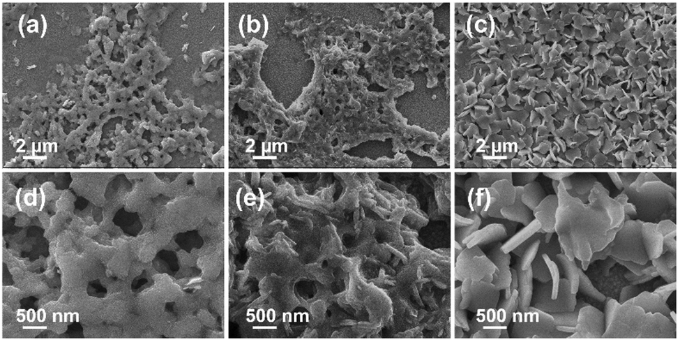 | ||
| Fig. 1 FESEM images of the films after the sequential thermo-reducing process with reducing agents: (a and d) HH, (b and e) HMC and (c and f) HDC. | ||
Furthermore, by performing material analysis using energy-dispersive X-ray spectroscopy (EDS, Table S1, ESI†) and FESEM, X-ray diffractometry (XRD, Fig. S1a, ESI†), UV-vis spectrometry (Fig. S1b, ESI†), and Raman shift spectroscopy (Fig. S1c, ESI†) for further material analysis, we found that: (i) using HH as a reducing agent, the deposited material was SnS2 film; (ii) using HMC as a reducing agent, the deposited material was a composite film containing SnS2 and SnS; and (iii) using HDC as a reducing agent, the deposited material was SnS. We noted that the interlacing form between the reducing agents and [Sn2S6]4− complex ions in the precursor film is the key cause of film composition and morphology tuning. As HH is a neutral reducing agent, there is poor interaction between HH and the [Sn2S6]4− complex in the precursor film, resulting in a random interlacing form, which leads to a deficiently reducing process. As HMC is a reducing agent, there is weak interaction between half-cationic HMC and the [Sn2S6]4− complex, resulting in a semi-ordered interlaced form, which leads to a partial reduction of SnS2 to SnS. As HDC is a reducing agent, there is a strong interaction between full-cationic HDC and the [Sn2S6]4− complex and a regular interlacing form, resulting in the complete reduction of SnS2 to SnS.
Investigation of surface morphology
Moreover, we noted that the ramping rate of the thermo-reducing process affects the interlacing form between the reducing agents and [Sn2S6]4− complexes, resulting in an adjustment in the crystal and film growth. Therefore, various thermal reducing processes with tailored temperature ramping rates were conducted to modify the morphologies of the SnS thin films using HDC as a reducing agent. As shown in Fig. 2, with temperature ramping rates of 5 °C min−1 (RR5), 10 °C min−1 (RR10), 30 °C min−1 (RR30), and 60 °C min−1 (RR60), the surface morphologies of the SnS films were seriously aggregated with small size nanoplate (Fig. 2a and b), uniform nanoplate film (Fig. 2c and d), semi-dense film composited with nanoplates (Fig. 2e and f) and dense film (Fig. 2g and h) morphologies, respectively (cross-sectional views are shown in Fig. S2, ESI†). For further material analysis, XRD, diffuse reflectance UV-vis-NIR spectroscopy, EDS, HRTEM, and SAED analyses were carried out. As shown in Fig. 3a, the diffraction patterns of the films (after calcination at 300 °C, 30 min in N2) with different ramping rates exhibited a 100% intensity peak (2θ = 32°), indexed to the (040) reflection of orthorhombic (OR) Pnma SnS (JCPDS card No. 00-014-0620).26 In the absorption spectrum of each film (shown in Fig. 3b), absorption peaks under 1000 nm and weaker absorption edges between 1100 and 1150 nm were obtained, which corresponded to a direct bandgap of approximately 1.22 eV and an indirect bandgap of approximately 1.11 eV for the SnS materials.26 The Raman shift spectrum of each film also certified that the films deposited with different ramping rates were SnS (Fig. 3c).6 The characteristic peaks observed at 95, 161, 183, and 220 cm−1 were assigned to SnS, and the peak at 313 cm−1 corresponds to the SnS2 phase. The EDS analysis applied using TEM exhibits an atomic ratio of 1![[thin space (1/6-em)]](https://www.rsc.org/images/entities/char_2009.gif) :1 between Sn and S for the films even with different surface morphologies (Table S2, ESI†).
:1 between Sn and S for the films even with different surface morphologies (Table S2, ESI†).
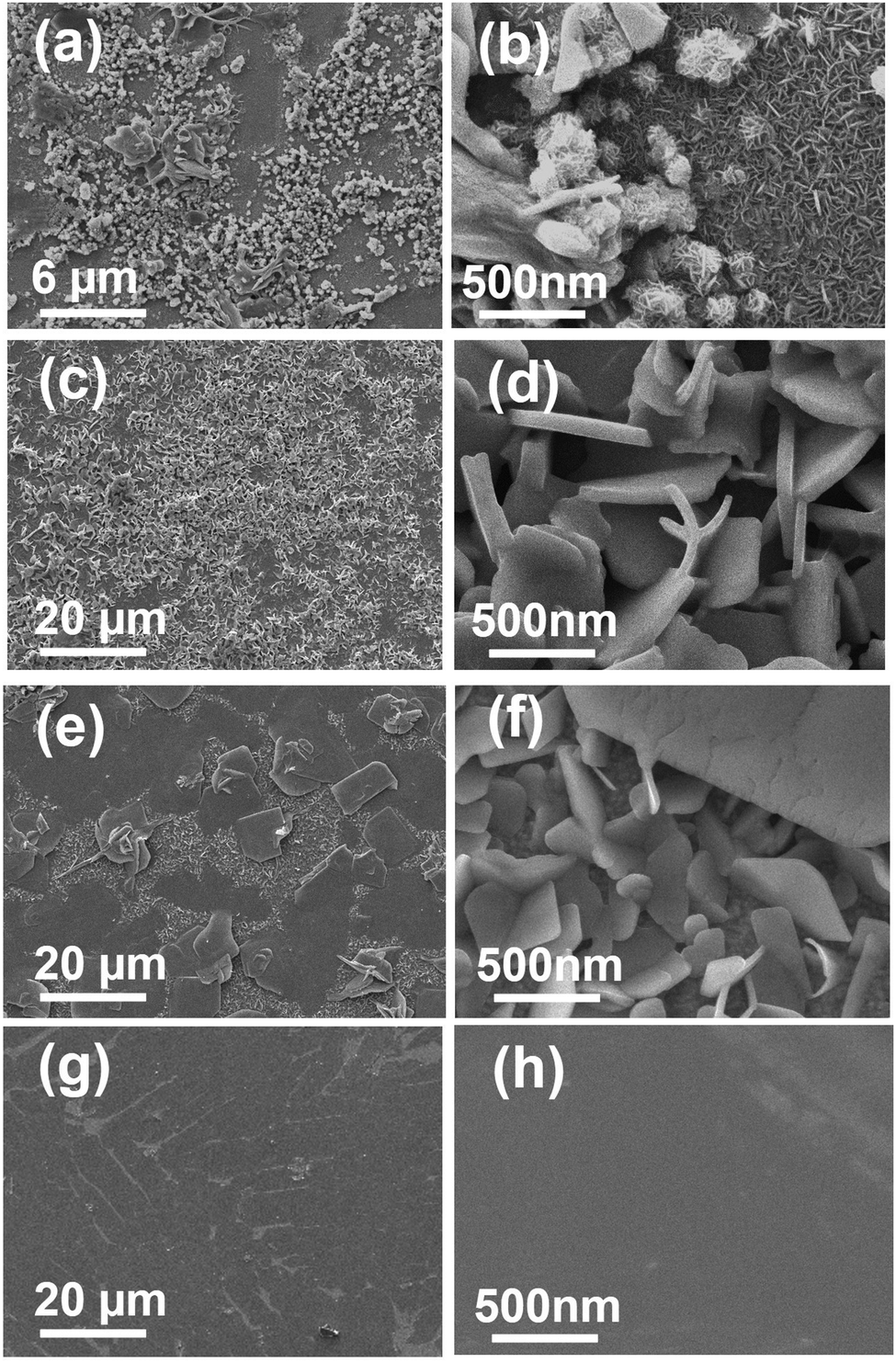 | ||
| Fig. 2 FESEM images of the SnS films with temperature ramping rates of (a and c) 5 °C min−1, (b and d) 10 °C min−1, (e and g) 30 °C min−1 and (f and h) 60 °C min−1. | ||
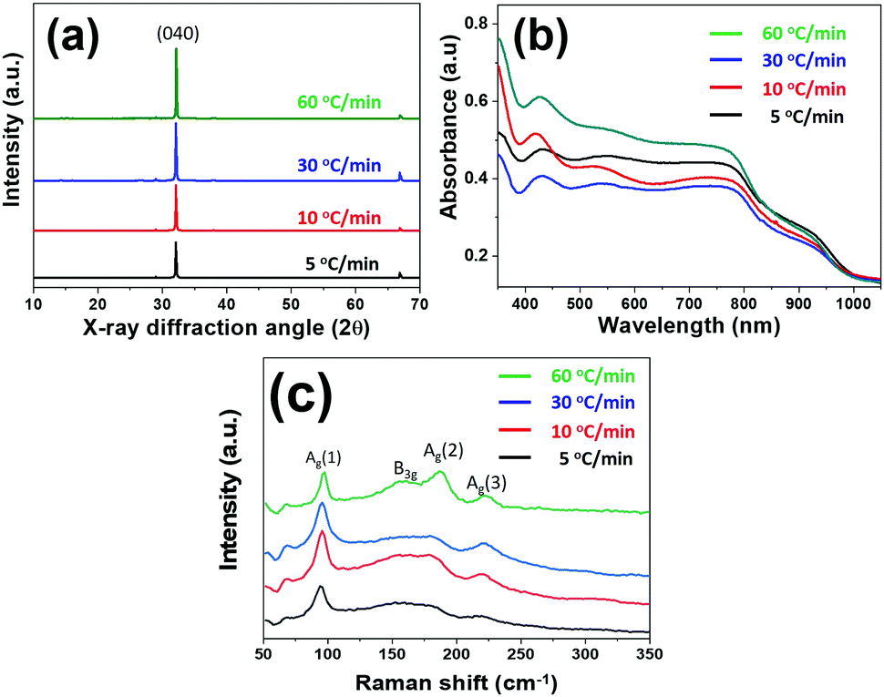 | ||
| Fig. 3 (a) XRD patterns, (b) UV-vis spectra and (c) Raman shift spectra of the spin-coating deposited SnS films with different temperature ramping rates. | ||
The structural details of the SnS thin films with a ramping rate of 5 °C min−1, 10 °C min−1 and 60 °C min−1 were further examined by HRTEM and SAED (Fig. S3, ESI†). SAED patterns of all the films reveal single-crystallinity due to the well-ordered dot pattern, which matches the list of reflections of OR-SnS bulk (JCPDS card No. 00-014-0620). The X-ray diffractogram (Fig. 1c) of the capillary powder sample is also consistent with the crystallography for OR-SnS bulk. Based on the above material and structural characterizations, we noted that the four kinds of SnS films had the same nanocrystal structures but different surface morphologies. Further photocurrent response analyses were carried out to assess the material's potential for photoelectronic applications.
Photo responsivity of the SnS films
Morphology-controllable SnS thin films were further prepared on the FTO surface, and were evaluated in contact with a solution of 0.1 M Eu(NO3)3 (Eu3+ acts as a sacrificial oxidant), with a Pt-mesh counter electrode and a Ag/AgCl electrode as a reference electrode under 1 Sun chopped illumination. A cathodic photocurrent showed that all SnS films exhibited p-type behavior due to photocurrent increment at negative potentials of −200 mV vs. Ag/AgCl (Fig. S4, ESI†) under chopped white-light illumination. Fig. 4a shows the instantaneous photocurrent response of the four kinds of SnS thin films under 1 Sun chopped illumination. Chronoamperometric experiments yielded photocurrents of the SnS films with ramping rates; RR5, RR10, RR30 and RR60 corresponded to 82.5 μA cm−2, 204.3 μA cm−2, 102.2 μA cm−2 and 70.2 μA cm−2 at an applied bias of −400 mV vs. Ag/AgCl. The uniform nanoplate film (RR10) showed the best photo responsivity in the test of vertical electron transfer through the SnS films, and the dense film (RR60) showed the worst photocurrent. The seriously aggregated film (RR5) and semi-dense film (RR30) showed intermediate photocurrent. We note that the photoactive area and internal resistance were the reasons for the photo responsivity difference among the four kinds of SnS films. The uniform nanoplate film has appropriate coverage and morphology to absorb light, and a good electron transfer channel (most of the nanoplates were vertically grown on the substrate), resulting in the highest photocurrent. Although the dense film has excellent coverage for absorbing light, it is a multi-layered structure of large SnS plates (Fig. S2d, ESI†), which is not suitable for vertical electron transfer to the electrode.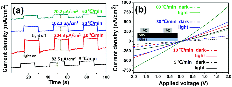 | ||
| Fig. 4 Photo responsivity of SnS films with different ramping rates: (a) chronoamperometric experiments yielded photocurrents and (b) photo-response I–V measurements (inset is the device structure). | ||
Moreover, the photo-response I–V measurements were collected for the four kinds of SnS films to evaluate their potential in other photoelectronic applications (the device structure is shown in Fig. 4b inset), such as photodetectors and photo-transistors. As shown in Fig. 4b, both the dark current (dot line) and photocurrent (solid line) of the dense film were much higher than those of the other films (related to 2 V). Surface morphology is the primary reason for the current difference, since the dense film provides a continuous channel for electron transfer.
Conclusions
In summary, morphology-controllable SnS films were deposited using the spin-coating route by tailoring the ramping rate of the thermo-reduction process. A fast-ramping rate of the thermo-reduction process restrains material aggregation and leads to a quick reduction reaction resulting in retained morphology of the precursor films in a dense form. A slow ramping rate brings about material aggregation due to a sluggish reducing reaction, resulting in nanostructured morphology. With careful material analysis, it is found that the deposited films with different temperature ramping rates have the same crystal structure but different surface morphology. Further photoresponse chronoamperometric experiments and I–V measurements indicate that the different morphology SnS films have the potential for multifarious photoelectronic applications, such as photovoltaics, photodetectors, and photo-transistors, which are the goals for our future works.Author contributions
Hui Liang: materials synthesis, fabricated the devices, and carried out FESEM, Raman spectroscopy and AFM; Bingchen Li: materials synthesis, fabricated the devices, and carried out TEM, SEAD, XRD and UV-vis spectroscopy; Gangri Cai: provided guidance in experimental design and understanding the phenomena, supervised the entire research programme and writing; Song Xue: provided guidance in experimental design and understanding the phenomena, and supervised the entire research programme.Conflicts of interest
There are no conflicts to declare.Acknowledgements
This research was supported by the Tianjin Science and Technology Commission (Natural science foundation project 20JCYBJC00420 and 18JCZDJC97000).Notes and references
- Y. Bao, P. Song, Y. Liu, Z. Chen, M. Zhu, I. Abdelwahab, J. Su, W. Fu, X. Chi, W. Yu, W. Liu, X. Zhao, X.-H. Xu, M. Yang and K. P. Loh, Nano Lett., 2019, 19, 5109–5117 CrossRef CAS PubMed.
- K. C. Kwon, Y. Zhang, L. Wang, W. Yu, X. Wang, I.-H. Park, H. S. Choi, T. Ma, Z. Zhu, B. Tian, C. Su and K. P. Loh, ACS Nano, 2020, 14, 7628–7638 CrossRef CAS PubMed.
- G. Liu, Y. Li, B. Li, H. Tian, C. Fan, Y. Zhang, Z. Hua, M. Wang, H. Zheng and E. Li, J. Mater. Chem. C, 2018, 6, 10036–10041 RSC.
- H. Tian, X. Meng, J. Yang, C. Fan, S. Yuan, X. An, C. Sun, Y. Zhang, M. Wang, H. Zheng, Z. Wei and E. Li, ACS Appl. Nano Mater., 2020, 3, 6847–6854 CrossRef CAS.
- J. R. Brent, D. J. Lewis, T. Lorenz, E. A. Lewis, N. Savjani, S. J. Haigh, G. Seifert, B. Derby and P. O’Brien, J. Am. Chem. Soc., 2015, 137, 12689–12696 CrossRef CAS PubMed.
- S. D. Tilley, Adv. Energy Mater., 2019, 9, 1802877 CrossRef.
- K. T. Ramakrishna Reddy, N. Koteswara Reddy and R. W. Miles, Sol. Energy Mater. Sol. Cells, 2006, 90, 3041–3046 CrossRef CAS.
- D. Ding, T. Rath, L. Lanzetta, J. Manuel Marin-Beloqui and S. A. Haque, ACS Appl. Energy Mater., 2018, 1, 3042–3047 CrossRef CAS.
- Q. Peng, S. Zhang, H. Yang, B. Sheng, R. Xu, Q. Wang and Y. Yu, ACS Nano, 2020, 14, 6024–6033 CrossRef CAS PubMed.
- J. W. Kim, N. H. Cho, Y.-C. Lim, S. W. Im, J. H. Hana and K. T. Nam, Mater. Adv., 2021, 2, 6988–6995 RSC.
- D. P. McMeekin, Z. Wang, W. Rehman, F. Pulvirenti, J. B. Patel, N. K. Noel, M. B. Johnston, S. R. Marder, L. M. Herz and H. J. Snaith, Adv. Mater., 2017, 29, 1607039 CrossRef PubMed.
- L. Lei, M. Li, D. M. Grant, S. Yang, Y. Yu, J. A. Watts and D. B. Amabilino, Chem. Mater., 2020, 32, 5958–5972 CrossRef CAS.
- N. K. Reddy, M. Devika, Q. Ahsanulhaq and K. R. Gunasekhar, Cryst. Growth Des., 2010, 10, 4769–4772 CrossRef.
- S. G. Hickey, C. Waurisch, B. Rellinghaus and A. Eychmuller, J. Am. Chem. Soc., 2008, 130, 14978–14980 CrossRef CAS PubMed.
- V. G. Pol, S. V. Pol and A. Gedanken, Langmuir, 2008, 24, 5135–5139 CrossRef CAS PubMed.
- S. Boonsalee, R. V. Gudavarthy and E. W. Bohannan, J. A. Chem. Mater., 2008, 20, 5737–5742 CrossRef CAS.
- E. C. Greyson, J. E. Barton and T. W. Odom, Small, 2006, 2, 368 CrossRef CAS PubMed.
- H. H. Park, R. Heasley, L. Sun, V. Steinmann, R. Jaramillo, K. Hartman, R. Chakraborty, P. Sinsermsuksakul, D. Chua, T. Buonassisi and R. G. Gordon, Prog. Photovoltaics, 2015, 23, 901–908 CAS.
- V. Steinmann, R. Jaramillo, K. Hartman, R. Chakraborty, R. E. Brandt, J. R. Poindexter, Y. S. Lee, L. Sun, A. Polizzotti and H. H. Park, Adv. Mater., 2014, 26, 7488–7492 CrossRef CAS PubMed.
- P. Sinsermsuksakul, L. Sun, S. W. Lee, H. H. Park, S. B. Kim, C. Yang and R. G. Gordon, Adv. Energy Mater., 2014, 4, 1400496 CrossRef.
- H.-S. Yun, B.-w. Park, Y. C. Choi, J. Im, T. J. Shin and S. I. Seok, Adv. Energy Mater., 2019, 9, 1901343 CrossRef.
- S. Gedi, V. R. Minnam Reddy, T. R. R. Kotte, Y. Park and W. K. Kim, Appl. Surf. Sci., 2019, 465, 802–815 CrossRef CAS.
- R. Carrizo, D. Ramírez, L. Hernández, G. Lobos, P. Häberle, E. A. Dalchiele and G. Riveros, ChemElectroChem, 2019, 6, 1047–1056 CrossRef CAS.
- M. Patel and A. Ray, ACS Appl. Mater. Interfaces, 2014, 6, 10099–10106 CrossRef CAS PubMed.
- P. D. Antunez, D. A. Torelli, F. Yang, F. A. Rabuffetti, N. S. Lewis and R. L. Brutchey, Chem. Mater., 2014, 26, 5444–5446 CrossRef CAS.
- Y. Dong, G. Cai, Q. Zhang, H. Wang, Z. Sun, H. Wang, Y. Wang and S. Xue, Chem. Commun., 2018, 54, 1992–1995 RSC.
- R. E. Banai, M. W. Horn and J. R. S. Brownson, Sol. Energy Mater. Sol. Cells, 2016, 150, 112–129 CrossRef CAS.
Footnotes |
| † Electronic supplementary information (ESI) available: Detail experiments; XRD pattern; UV–vis spectrum; Raman spectrum; SEM and HRTEM images; EDX analysis data. See DOI: 10.1039/d1ma01073e |
| ‡ These authors contributed equally to this work |
| This journal is © The Royal Society of Chemistry 2022 |