
 Open Access Article
 This Open Access Article is licensed under a
 Creative Commons Attribution 3.0 Unported Licence
Tailoring the molecular weight of polymer additives for organic semiconductors
Zhengran
He
 *a,
Ziyang
Zhang
b and
Sheng
Bi
*c
*a,
Ziyang
Zhang
b and
Sheng
Bi
*c
aDepartment of Electrical and Computer Engineering, The University of Alabama, Tuscaloosa, AL 35487, USA. E-mail: zhe3@crimson.ua.edu
bDepartment of Electrical Engineering, Columbia University, New York City, NY 10027, USA
cKey Laboratory for Precision and Non-traditional Machining Technology of the Ministry of Education, Dalian University of Technology, Dalian, Liaoning 116024, China. E-mail: bish@dlut.edu.cn
First published on 12th January 2022
Abstract
A binary system comprising both an organic semiconductor and a polymer additive has attracted extensive research interests due to its great potential for use in high-performance, solution-processable electronic devices on flexible substrates. The molecular weight of polymer additives plays a critical role in modulating the crystal growth, enabling phase segregation, optimizing thin film morphology, and improving the charge transport of organic semiconductors. Here, we provide an in-depth review of the recent progress in studying amorphous and semicrystalline polymeric additives, including polystyrene, poly(α-methylstyrene), polymethyl methacrylate, and polyethylene oxide, and fully discuss the effect of the different polymer molecular weights on semiconductor crystallization, active layer composition, and the electrical performance of miscellaneous organic semiconductors. Using the representative examples of 6,13-bis(triisopropylsilylethynyl)pentacene (TIPS pentacene), 2,7-dioctyl[1]benzothieno[3,2-b][1]benzothiophene (C8-BTBT), and 2,8-difluoro-5,11-bis(triethylsilylethynyl)anthradithiophene (diF-TES-ADT), this work sheds light on utilizing these universal polymers with varying molecular weights to powerfully manipulate the charge transport of other high-mobility, solution-processable organic semiconductors.
 Zhengran He | Dr Zhengran He received his BS degree from the School of Electronic Engineering at Xi’an Jiaotong University, China, and PhD degree in Electronic Engineering at the University of Alabama, USA. His current research interests are high performance of optoelectronic transistors and the development of physics in organic–inorganic electronic devices. |
 Ziyang Zhang | Mr Ziyang Zhang received his BS degree from the School of Electronic Engineering at Xi’an Jiaotong University, China, and MS degree in Electronic Engineering at Columbia University, USA. His current research interests are organic electronics, machine learning and composites. |
 Sheng Bi | Dr Sheng Bi is an associate professor in the School of Mechanical Engineering, Dalian University of Technology (DUT), China. He received his BS degree from the School of Physics at Dalian University of Technology in 2011 and PhD degree in electronic engineering at University of Alabama, USA, in 2016. His current research is focused on the behaviors of excited states in the light-emitting diodes based on organic materials. |
1. Introduction and background
1.1 Recent progress in flexible electronics
In recent years, research on flexible electronics has witnessed rapid progress.1–11 Great efforts have been made to study solvent choices, controllable crystallization, charge carrier mobilities, and organic electronic device applications of solution-processed small-molecular organic semiconductors, such as 6,13-bis(triisopropylsilylethynyl)pentacene (TIPS pentacene),12–17 2,7-dioctyl[1]benzothieno[3,2-b][1]benzothiophene (C8-BTBT),18–21 2,5-di-(2-ethylhexyl)-3,6-bis(5′′-n-hexyl-2,2′,5′,2′′]terthiophen-5-yl)-pyrrolo[3,4-c]pyrrole-1,4-dione (SMDPPEH)22–24 and 2,8-difluoro-5,11-bis(triethylsilylethynyl)anthradithiophene (diF-TES-ADT).25–28 For instance, based on the structural engineering of the organic semiconductor pentacene, the herringbone packing patterns in TIPS pentacene are interrupted by the attachment of the bulky side chains, which improves the solubility of TIPS pentacene in organic solvents.29,30 The enhanced π–π stacking in TIPS pentacene is attributed to higher charge transport.31 These research endeavors have opened up vast opportunities for organic semiconductors to be applied in high performance organic electronic devices such as organic thin film transistors,32–35 organic gas sensors,36–38 photovoltaic devices39–41 and logic circuits.42–44 In this section, we will review the important studies that investigated the solution processability and charge carrier mobility of organic semiconductor based thin film transistors, as well as their application in fabricating organic gas sensors.First, research studies have been devoted to exploring the solvent possibilities of organic semiconductors, allowing the modulation of semiconductor morphology and charge transport.45–47 For instance, Kim et al. investigated the effect of different solvents on the thin film morphology and crystallinity of TIPS pentacene.48 Solvents with high boiling points such as chlorobenzene and xylene resulted in dendritic morphology with higher crystallinity, whereas solvents with low boiling points such as chloroform led to an amorphous film with low crystallinity. Choi et al. studied the correlation between the solvent boiling point, grain size and charge transport.29 Spin coating TIPS pentacene from chlorobenzene with a high boiling point produced crystals with a large grain size and high crystallinity, yielding a mobility that is 5 orders of magnitude higher than that from a low boiling point solvent such as chloroform. Hwang et al. reported the effect of different solvents including chlorobenzene and tetralin on the vertical phase segregation and compositional structure of TIPS pentacene/polymer blends.49 Distinct phase segregation and enhanced crystallization were observed based on the solvent tetralin, attributed to higher mobility values. Ozorio et al. discovered how the different solvent choices impacted the vertical phase segregation and charge transport in the TIPS pentacene/poly(3-hexylthiophene) (P3HT) blends.50 Solvent trichlorobenzene caused a moderate vertical phase segregation between TIPS pentacene and P3HT and gave rise to optimized TIPS pentacene film morphology and enhanced P3HT ordering, which yielded an output current that is 39 times larger as compared to the counterpart based on other solvents such as chloroform and toluene.
Besides, highly effective alignment methods have been shown to enhance the charge carrier mobilities of the organic semiconductors close to or over 10 cm2 V−1 s−1. While miscellaneous alignment methods have been reported, they can be mainly summarized into the categories of blading coating, substrate patterning, slot-die coating and controlled evaporation based methods. First, blade coating based methods involve either a running blade over a stationary substrate or a stationary blade over a moving substrate.51–54 The resultant film thickness is determined by the gap between the blade and substrate, the coating speed and the viscoelastic properties of the solution. Solution shearing, as an enhanced version of the blade coating method, involves the use of a tilted blade to deposit the organic semiconductor solutions.55–59 Solution shearing has been reported to effectively tune the molecular packing, manipulate the crystal alignment and control the thin film morphology of organic semiconductors.60,61 Peng et al. demonstrated a “dual solution-shearing” method and reported a mobility of 10 cm2 V−1 s−1 using the organic crystals of 2,7-didecyl[1]benzothieno[3,2-b][1]benzothiophene (C10-BTBT).62 Bilgaiyan et al. reported the solution shearing of a 6,6 bis(trans-4-butylcyclohexyl)-dinaphtho[2,1-b:2,1-f]thieno[3,2-b]thiophene (4H-21DNTT) organic semiconductor based thin film transistor and obtained a mobility of 10.5 cm2 V−1 s−1.63 The 4H-21DNTT based CMOS inverter circuit showed sharp switching behaviors with a 31.5 signal gain. Second, substrate patterning based methods involve the tuning of substrate wettability by using surfactant treatment and/or photolithography patterning, which can effectively confine the deposition of organic semiconductor solutions as well as the subsequent crystal growth and alignment. Zhao et al. demonstrated an “asymmetric-wettability topographical template” to control the ordered crystallization of 2,7-dioctyl[1]benzothieno[3,2-b][1]benzothiophene (C8-BTBT), giving rise to a mobility of 8.7 cm2 V−1 s−1.64 Shen et al. reported the controlled crystallization and morphologies of the C8-BTBT organic semiconductor via tuning substrate wettability with soluble polymer films as a modification layer.65 The resultant C8-BTBT film with optimized grain boundary and domain size exhibited a mobility higher than 7 cm2 V−1 s−1. Deng et al. reported a “channel-restricted meniscus self-assembly (CRMS)” method, which combined photolithography patterning and dip coating, to grow uniform 2,6-diphenylanthracene (DPA) single crystal arrays.66 The photoresist patterning confined the lateral growth of DPA single crystals, leading to a mobility of 30.3 cm2 V−1 s−1. Third, slot die coating based methods deposit the organic semiconductor solution onto a moving substrate directly through a coating head at a tunable rate.67–70 Lin et al. demonstrated highly ordered single crystalline TIPS pentacene films by using a roll-to-roll slot die coating method, and reported a mobility of 4.2 cm2 V−1 s−1 for pristine TIPS pentacene.71 Xie et al. reported a roll-to-roll slot die coating method to fabricate thin film transistors.72 With Ag nanowires deposited by using the R2R coating method as the gate electrode, the C8-BTBT/polystyrene (PS) based transistor showed a mobility of 18.3 cm2 V−1 s−1. Fourth, controlled evaporation based methods involve the tuning and control of the solution flow behavior and evaporation rate in order to modulate the deposition and growth of organic semiconductors.73–75 Wang et al. reported a “Marangoni effect-controlled growth” method to grow a highly oriented C8-BTBT film with a herringbone stacking structure.76 A high mobility of 25 cm2 V−1 s−1 was obtained from the C8-BTBT based transistors incorporating a long channel length. Soeda et al. reported the growth of an aligned organic semiconductor 3,11-didecyldinaphtho[2,3-d:2′,3′-d′]benzo[1,2-b:4,5-b′]dithiophene (C10-DNBDT) with controlled solvent evaporation.77 By holding the C10-DNBDT solution at a moving blade edge, continuous solvent evaporation and supply at the same rate gave rise to aligned crystals extending in inches and a mobility of 10 cm2 V−1 s−1.
The exceptional high mobilities present great opportunities for the organic semiconductors to be implemented in high performance organic electronic devices such as gas sensors. Manoli et al. demonstrated a P3HT thin film transistor based gas sensor for detecting acetone, ethanol and n-butanol vapors.78 When exposed to the vapors, the P3HT thin film transistors showed a decreased drain current as a result of the enlarged potential barrier at the P3HT grain boundaries as charge trapping. Seo et al. reported a 5,11-bis(triethylsilylethynyl)anthradithiophene (TES-ADT) thin film transistor based gas sensor for detecting NO2 gas.79 Exposure to 0 ppm to 100 ppm NO2 gas caused accumulation of charge carriers and thereby led to an increase in the on-current. Hou et al. studied the effect of grain boundaries on the sensing performance of TIPS pentacene transistor based gas sensors.80 Solvent vapor annealing with toluene gave rise to a large density of grain boundaries and thereby higher sensitivity when NO2 gas diffused into the grain boundaries and caused a more pronounced current increase. Shao et al. compared the effect of different solvents on the performance of TIPS pentacene transistor based gas sensors.81 Spin coating TIPS pentacene in solvent o-xylene was observed to yield abundant grain boundaries and thereby enhanced gas sensing performance of NO2.
1.2 Challenges in controlling organic semiconductor crystallization
Despite the major advantages of organic semiconductors such as high mobility and solution processability, the crystallization of organic semiconductors based on solution processing can still be difficult to maneuver.82–86 In this section, we employ TIPS pentacene as a benchmark semiconductor to discuss the main challenges that can limit the implementation of organic semiconductors in organic electronic applications. These challenges include crystal misorientation, thermal cracks and grain boundaries, which will be discussed in greater detail below.First, when drop cast in solution, TIPS pentacene forms dendritic patterns of crystal ribbons, which can be characterized by considerable crystal misorientation and film gaps.87–98 In a pivotal study conducted by Chen and coworkers,99 the misorientation angle θ was measured between the TIPS pentacene crystal long axis and the direction from source to drain contact electrodes in the transistor device. This angle was used as the baseline to evaluate the crystal misorientation induced mobility variations. When the smallest angle θ corresponded to the crystal orientation being parallel with the source/drain electrode direction, the largest hole mobility of 0.04 cm2 V−1 s−1 was measured from the TIPS pentacene based transistors. When the crystal orientation bridged the source/drain electrode direction at the largest angle θ, the smallest mobility of 0.004 cm2 V−1 s−1 was obtained, which showed that the mobility dropped by 10 fold. Similarly, such crystal misorientation has been reported in two other p-type organic semiconductors, i.e. 5,6,11,12-tetrachlorotetracene100 and 2,5-di-(2-ethylhexyl)-3,6-bis(5′′-n-hexyl-2,2′,5′,2′′] terthiophen-5-yl)-pyrrolo[3,4-c]pyrrole-1,4-dione (SMDPPEH),101 when grown from a single chloroform solvent via the drop casting method.
Besides, the charge transport in the organic semiconductors may be impeded by large-scale thermal cracks, which occur after the semiconductors are exposed to elevated temperature. Chen et al. reported that when TIPS pentacene was heated at 150 °C, the organic semiconductors started to show thermal cracks,102 which was linked to the lower surface energy in various planes of the semiconductor. While pristine TIPS pentacene based transistors exhibited a hole mobility of up to 1 cm2 V−1 s−1 in this study, the counterpart with the occurrence of thermal cracks showed a much lower hole mobility of up to 0.2 cm2 V−1 s−1, which counts for a significant reduction in mobility by 80%. The generation of thermal cracks in TIPS pentacene was also reported in a later study by Asaree-Yeboah et al. who applied a temperature gradient technique in order to align the crystal growth direction of TIPS pentacene.103 These thermal cracks extended to a few hundred micrometers, posing a barrier for efficient charge transport in TIPS pentacene. Despite exerting a blocking effect on charge transport, thermal cracks at the domain boundaries have been reported to generate deep electron traps and enhance the stability of TIPS pentacene based thin film transistor photo responsivity. Cho et al. reported that thermal annealing induced cracks at the domain boundary of TIPS pentacene films and related both the stable photoresponsive characteristics and lower charge carrier mobility to the corresponding deep electron traps.104
Moreover, the crystal growth of organic semiconductors can result in small grain widths.105–109 Because crystalline defects and charge trap sites are prevalent at the grain boundaries, small grain widths can be generally associated with a greater amount of defects and traps, which charge carriers must circumvent along the charge transport pathway.110–120 If we assume that the channel length L is equal to the length of crystals, or LG, plus the length of crystal boundary, or LGB, then we have:
| L = (n − 1)LGB + nLG | (1) |
 | (2) |
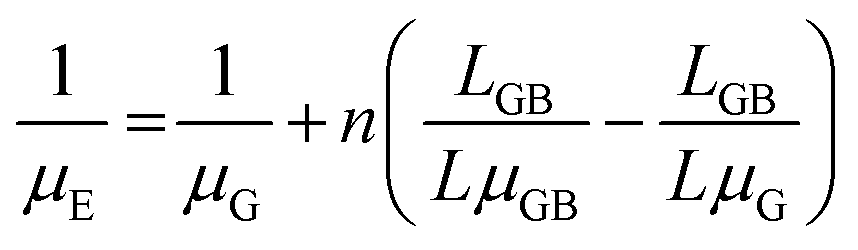 | (3) |
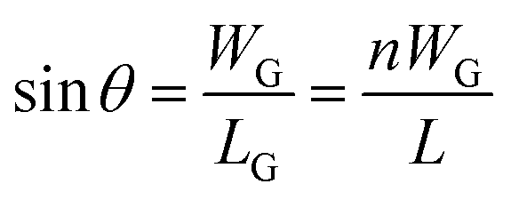
The length of crystals can be correlated with the width of grains, or WG, via the following equation:
 | (4) |
 | (5) |
By assigning 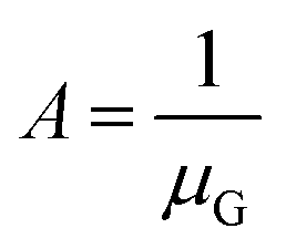 and
and  , we have:
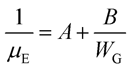 | (6) |
Eqn (6) shows a clear correlation between the width of grains and the effective mobility, which states that a small grain width from the solution-processed organic semiconductors can result in lower effective mobility.
2. Benefits of polymer-modulated crystallization
Miscellaneous polymer additives have been extensively studied for mixing with solution processable, small molecular organic semiconductors.124–129 When the polymer additives are mixed with semiconducting small molecules, the resultant binary system can benefit from improved semiconductor morphology uniformity,130–134 phase segregation-enhanced charge transport135–139 and operational device stability.140–147 In this section, we will briefly discuss the benefits of mixing organic semiconductors with different categories of polymer additives, including amorphous polymers, conjugated polymers and semicrystalline polymers.2.1. Amorphous polymers
Mixing organic semiconductors with amorphous polymers can help improve the thin film morphology uniformity and, more importantly, can promote the formation of orientated crystals and reduce crystal misorientations.148,149 For example, pristine TIPS pentacene has been reported to form random crystal ribbons or dendritic patterns of crystals by multiple groups.150–152 The mixing of TIPS pentacene with amorphous polymer, such as poly(α-methylstyrene) (PαMS), can significantly reduce crystal misorientation.153 He et al. reported that when drop cast in the solvent of toluene, the TIPS pentacene pristine film exhibited a large misorientation angle of 43.9° ± 27.8°, whereas the addition of PαMS with TIPS pentacene strongly prevented such random crystal morphology and reduced the misorientation angle to 2.2° ± 1°.30Another major benefit that rises from blending organic semiconductors with amorphous polymers is the occurrence of phase segregation between the organic semiconductor and polymer additive.154–160 This phase segregation can include lateral phase segregation, vertical phase segregation, or a mixture of both. In particular, vertical phase segregation between the organic semiconductor and amorphous polymer can facilitate the formation of a more concentrated semiconductor layer at the interface between the active layer and the dielectric layer, expediting charge transport of the organic semiconductor. Also, a polymeric encapsulation layer that forms as a result of the vertical phase segregation can protect the semiconductor active layer from being exposed to the ambient environment, enhancing the operational stability of the thin film transistors.161,162
2.2 Conjugated polymers
When organic semiconductors are blended with conjugated polymers, the binary system can give rise to intermolecular interactions between these two components.163–168 For example, Chen et al. reported that when two different types of conjugated polymers, including P3HT and regiorandom pentacene–bithiophene polymer (PnBT–RRa), were mixed with TIPS pentacene, the resultant binary system exhibited tunable intermolecular interactions that arise from both π–π interactions and hydrophobic interactions. The different extent of molecular structural similarity between TIPS pentacene and the conjugated polymer additives determines the intensity of intermolecular interactions. A small structural similarity between TIPS pentacene and P3HT yielded less intimate mixing and intermolecular interactions, leading to a polymorph with greater changes in the cell parameters. A higher similarity between TIPS pentacene and PnBT–RRa resulted in more intimate mixing, stronger interactions, and a polymorph with smaller changes in the cell parameters. Such differences further modulate the thin film morphology and confine charge transport in the organic semiconductor.89 Depending on the different types of conjugated polymers and extent of intermolecular interactions, the TIPS pentacene crystalline morphology can range from straight crystal needles to grass-like ribbons. Simultaneously, the conjugated polymer may exhibit cocrystallization along with the organic semiconductor. Thereby, each conjugated polymer yielded distinct modes of crystallization behavior and charge transport.2.3 Semicrystalline polymers
When compared to the amorphous and conjugated counterparts, semicrystalline polymers169–175 can preserve their own nucleation and crystallization events, which are independent of and also competing with the nuclei formation and crystal growth of the organic semiconductors. In the meanwhile, semicrystalline polymers are still partially amorphous, allowing the modification of diffusivity and surface energies of the organic semiconductor facets similar to amorphous polymers. Unlike conjugated polymers, semicrystalline polymers eliminate the polymer-caused π–π interactions as described above, which may be a complicated process unwanted in some organic semiconductor applications. Thereby, semicrystalline polymers provide a novel pathway to guide organic semiconductor crystallization and tune its morphology from an unexplored perspective.3. Overview of polymers with varying molecular weights
In this section, we will provide an overview of the important studies that report mixing organic semiconductors with polymeric additives with different molecular weights, in order to tune the crystal growth, thin film morphology, phase segregation, and charge transport. These polymer additives will be discussed in the following category: PαMS, PS, polymethyl methacrylate (PMMA) and polyethylene oxide (PEO); their molecular structures are shown in Fig. 1(a–d). Fig. 1(e–h) show the molecular structures of the various organic semiconductors mixed with the polymer additives in this section. | ||
| Fig. 1 Molecular structures of the various polymer additives and small-molecular organic semiconductors discussed in this work, including (a) polystyrene (PS), (b) poly(α-methylstyrene) PαMS, (c) polymethyl methacrylate (PMMA), (d) polyethylene oxide (PEO), (e) poly(3-hexylthiophene) (P3HT), (f) 2,7-dioctyl[1]benzothieno[3,2-b][1]benzothiophene (C8-BTBT), (g) 6,13-bis(triisopropylsilylethynyl) pentacene (TIPS pentacene), and (h) 2,8-difluoro-5,11-bis(triethylsilylethynyl)anthradithiophene (diF-TES-ADT). | ||
3.1 Polystyrene with varying molecular weights
PS is an amorphous and thermoplastic polymer that finds extensive applications in miscellaneous semi-finished products such as plastic films and foams. PS has excellent electrical insulation properties and outstanding optical clarity as a result of its lack of crystallinity. Besides, PS is chemically resistant to diluted bases and acids, but can be attacked by hydrocarbon solvents and UV exposure. The stiffness of the PS polymer backbone results in brittle nature and low impact strength. Furthermore, PS has a low limit of upper temperature for continuous processing. When mixed with organic semiconductors, PS typically causes pronounced vertical phase segregation,129,176 enhances semiconductor wettability,177 modulates active layer structure and polymorph,178 reduces charge interfacial traps,179 and improves charge transport reproducibility.180Leonardi et al. reported the effect of PS additive with different molecular weights, including 3 K and 100 K, on the vertical phase segregation, thin film morphology and stability of a donor–acceptor random copolymer, i.e. PDPP-TT(1)-SVS(9).137 AFM images in Fig. 2 show a vertical phase segregation with a bottom PDPP-TT(1)-SVS(9) layer beneath a top PS layer, which could serve as an encapsulation layer and improve the stability of the transistor device. In particular, the PDPP-TT(1)-SVS(9)/PS blend film with the 3 K molecular weight exhibited a non-homogeneous surface, whereas the counterpart with the 100 K molecular weight showed a thicker PS layer with the existence of holes, which resulted from the increased viscosity of the blend solution. PDPP-TT(1)-SVS(9) based transistors with the addition of PS with 3K and 100K molecular weights demonstrated average mobilities of 0.22 cm2 V−1 s−1 and 0.10 cm2 V−1 s−1, respectively. The enhanced charge transport was a direct benefit from the passivation of surface hydroxyl groups by the vertically-segregated PS polymer additive.
 | ||
| Fig. 2 AFM images showing the topography of the PDPP-TT(1)-SVS(9)/PS mixture film, with different molecular weights of PS including (a) 3 K and (b) 100 K. Reproduced from ref. 181, with permission from Elsevier. | ||
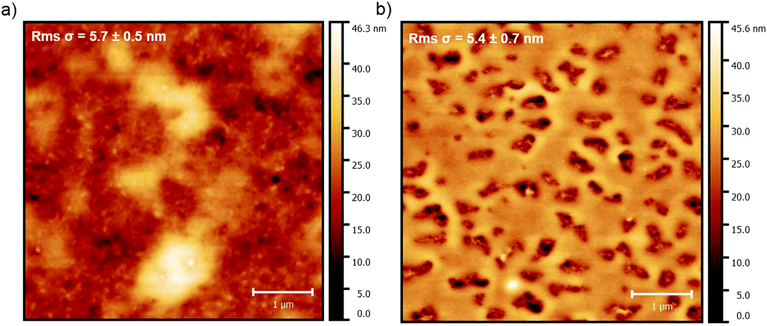
Niazi et al. studied the impact of PS additives with different molecular weights on the phase separation, composition and domain size of the organic semiconductor diF-TES-ADT.182 PS with different molecular weights including 2.2 K and 900 K was mixed with diF-TES-ADT. The mixture was deposited by using the blade coating method with a direction parallel with the source-to-drain electrodes. The thin film morphology of neat diF-TES-ADT and the diF-TES-ADT/PS mixture film is shown in the polarized optical images and AFM images in Fig. 3. It can be inferred that the film morphology and domain size depend on the molecular weight of PS. Besides, both phase segregation and active layer compositions were found to correlate to the molecular weight of PS. In particular, PS with a high molecular weight of 900 K caused the formation of a vertically-segregated bilayer structure: a top diF-TES-ADT layer and a bottom PS layer. Conversely, PS with a low molecular weight of 2.2K led to a mixture of diF-TES-ADT and PS in the top section. A thin film transistor incorporating the diF-TES-ADT/PS mixture as the active layer showed a mobility of up to 6.7 cm2 V−1 s−1 based on the high molecular weight PS, which is 50-times higher than that based on the low molecular weight counterpart. The high performance of the transistor devices was attributed to the single crystalline diF-TES-ADT layer with large domains as a result of vertical phase segregation.
 | ||
| Fig. 3 Polarized optical images and corresponding AFM images of (a) neat diF-TES-ADT, (b) diF-TES-ADT blended with PS with a low molecular weight of 2.2 K, and (c) diF-TES-ADT blended with PS with a high molecular weight of 900 K. The direction of blade coating was parallel with the direction from the source to drain contact electrodes. Reproduced from ref. 182, with permission from Springer Nature. | ||
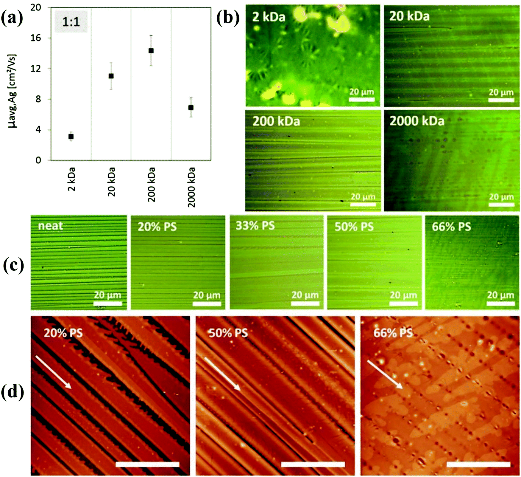
Haase et al. reported the addition of PS with different molecular weights in order to reduce the device-to-device mobility variation of the organic semiconductor C8-BTBT.183 Different molecular weights of the PS polymer including 2 K, 20 K, 200 K and 2000 K were tested on the thin film morphology of the organic semiconductor. PS with a low molecular weight resulted in a spherulitic growth of solution-sheared C8-BTBT films, whereas PS with a larger molecular weight yielded C8-BTBT ribbons with enhanced film coverage, as shown in the microscopic optical images in Fig. 4. Accordingly, the highest mobility of 14.4 cm2 V−1 s−1 was observed with PS with a molecular weight of 200 K, at an optimized blending ratio of 1![[thin space (1/6-em)]](https://www.rsc.org/images/entities/char_2009.gif) :1. Finally, distribution of saturation mobility was studied for thin film transistors based on neat C8-BTBT and the C8-BTBT/PS mixture in a 1:1 ratio. The addition of the PS polymer resulted in a much narrower distribution of mobility as well as reduced standard deviation.
:1. Finally, distribution of saturation mobility was studied for thin film transistors based on neat C8-BTBT and the C8-BTBT/PS mixture in a 1:1 ratio. The addition of the PS polymer resulted in a much narrower distribution of mobility as well as reduced standard deviation.
 | ||
| Fig. 4 Microscopic images of solution-sheared C8-BTBT films from blends based on different PS molecular weights, including 2 K, 20 K, 200 K and 2000 K. Reproduced from ref. 183, with permission from Wiley. | ||
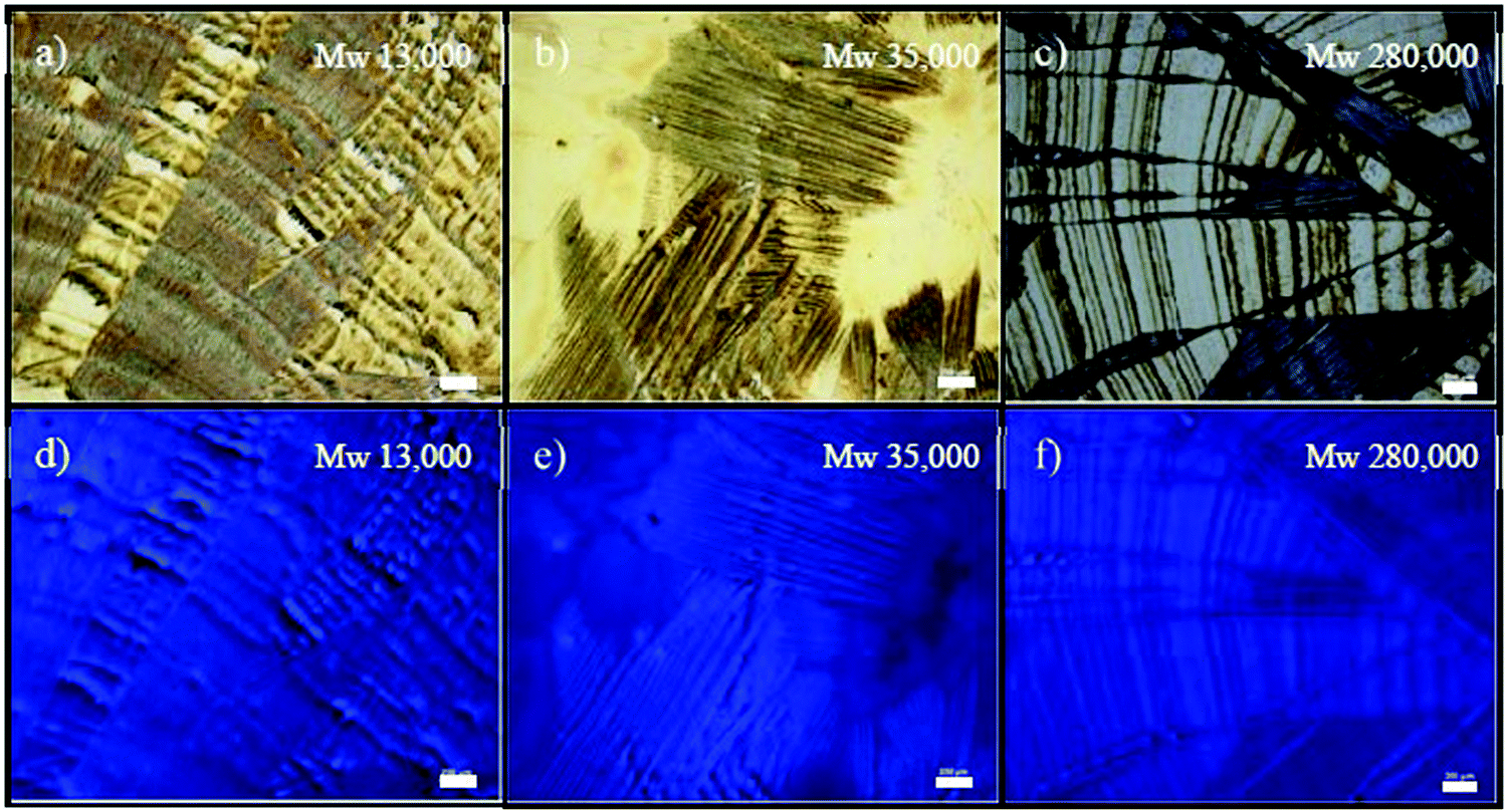
Singsumphan et al. studied the effect of PS molecular weight on the polymer viscosity and drop-cast thin film morphology of organic semiconductor 9,10-bis-2-[tris(1-methylethyl)silyl]ethynyl anthracene (TIPS-anthracene).184Fig. 5 shows the optical images and fluorescence images of drop cast TIPS-anthracene based on mixing with PS of different molecular weights including 13 K, 35 K and 280 K, respectively. For PS with a low molecular weight of 13 K, the mixed TIPS–anthracene exhibited a crystalline morphology of elongated needles. For PS with an intermediate molecular weight of 35 K, the needle shaped TIPS–anthracene crystals adopted alignment in different directions, indicating greater randomness of the thin film morphology. For PS with a high molecular weight of 280 K, the needle-like TIPS–anthracene crystals further suffered from reduced substrate coverage, which was caused by the high viscosity of PS and poor processability. This study indicated that tuning the polymer viscosity by employing polymer additives with different molecular weights can be a pathway to regulate the thin film morphology of organic semiconductors.
 | ||
| Fig. 5 (a–c) Optical images and (d–f) fluorescence images of TIPS–anthracene/PS blend films based on different PS molecular weights including 13 K, 35 K and 280 K. The scale bar is 200 μm. Reproduced from ref. 184, with permission from Elsevier. | ||
Rocha et al. studied the mixing of TIPS pentacene with PS with different molecular weights, including 2 K, 20 K, 200 K and 2000 K, to improve the binary system's miscibility and charge transport.185 At a mixing ratio of 1:1, the TIPS pentacene/PS mixture was deposited by using a solution shearing method. The resultant crystalline film exhibited different morphologies, dependent on different molecular weights of the PS polymer additive and different solution shearing speed. In particular, highly anisotropic crystalline ribbons and more isotropic spherulitic crystals were obtained based on low and high solution shearing speed, respectively. Electrical characterization results indicated that PS with a higher molecular weight yielded a higher charge carrier mobility as compared to the counterpart with 2 K molecular weight. The low mobility from low molecular weight PS can be attributed to the higher miscibility between PS and TIPS pentacene, preventing the phase segregation and the growth of highly crystalline TIPS pentacene ribbons. On the other hand, PS with a molecular weight larger than 20 K was observed to induce a phase segregation between TIPS pentacene and PS. The highest mobility of 12.3 cm2 V−1 s−1 was demonstrated based on the TIPS pentacene/PS mixture with a 20K molecular weight.
Han et al. reported the effect of different PS molecular weights on the response of P3HT based gas sensors.186 Two types of PS, including isotactic semicrystalline PS with molecular weights of 1.3 K, 250 K, 280 K and 290 K and amorphous PS with a molecular weight between 130 K and 290 K, were mixed with P3HT at a 4:1 ratio to form an active layer of the thin film transistors. When the P3HT based transistor devices were exposed to 10 ppm NH3 gas, the gas sensing response increased as the molecular weight of isotactic semicrystalline PS increased. In contrast, a much lower sensing response was observed for the counterpart based on the amorphous PS polymer additive. The enhanced sensing performance by the isotactic semicrystalline PS with a larger molecular weight was attributed to the formation of vertically-segregated, more continuous P3HT microstructures, which provide an undisrupted pathway for the transport of charge carriers in the transistor device. A mobility of 0.03 cm2 V−1 s−1 was reported from the P3HT/PS based transistors.
3.2 Poly(α-methylstyrene) with varying molecular weights
PαMS is an amorphous polymer with outstanding hardness, heat resistance and solvent resistance properties.187 While PαMS in general finds good solubility in both aromatic and halogenated solvents, only PαMS with a low molecular weight can be soluble in methyl ethyl ketone. The physical properties of PαMS such as solvent resistance depend on the amount of monomer and low molecular weight polymer in the compositions. Due to its relative brittleness and lower thermal stability (as compared to PS), the molecular weight of PαMS should be kept at a minimum value to enable any molding and extrusion processes to occur. As a result, it is desirable to set the molecular weight of PαMS at a lower limit, in order to render the polymer more useful physical properties. In the field of organic electronics, PαMS has been extensively studied for mixing with various organic semiconductors in order to improve the uniformity of thin film morphology,188 modulate semiconductor wettability,189 reduce crystal misorientation,30,190 control the formation of thermal cracks,191 enhance charge carrier mobilities,192,193 recover electrical performance,194 and improve the thin film transistor device stability.195Ohe et al. reported the impact of different molecular weights of the polymeric additive PαMS on phase segregation, thin film morphology and charge carrier mobility of the organic semiconductor TIPS pentacene.196 The different molecular weights of the polymeric additive PαMS included 2 K, 20 K, 60 K, 100 K and 800 K. Source and drain contact electrodes were prepatterned on the substrate covered with a cross-linked poly(vinyl phenol) gate dielectric layer. Then PαMS was mixed with TIPS pentacene at a 1:1 weight ratio in solution before being spin coated onto the source and drain electrodes. Electrical characterization results showed while the addition of PαMS with a low molecular weight of 2 K resulted in a low mobility, PαMS with a molecular weight above 20 K yielded a much higher mobility of 0.1 cm2 V−1 s−1. To study the composition in the vertical profile of the organic semiconductor film, time-of-flight secondary ion mass spectrometry was conducted on the TIPS pentacene/PαMS blends. The secondary Si− ions and SiH− ions were used to mark the existence of TIPS pentacene. The addition of a PαMS additive with a molecular weight of 2 K led to a homogeneous distribution of TIPS pentacene, whereas PαMS with a high molecular weight of 100 K promoted a vertical phase segregation between the polymer additive and TIPS pentacene. Furthermore, the polarized optical microscope images showed that the PαMS additive with a high molecular weight of 100 K enlarged the crystalline region on the surface. Flory–Huggins theory, which is indicative of the Gibbs free energy change upon mixing, was applied to understand phase segregation between TIPS pentacene and PαMS. Negative Gibbs free energy of mixing implies homogeneous mixing, whereas positive Gibbs free energy of mixing indicates that phase segregation can more easily occur. The low molecular weight PαMS resulted in a negative value of ΔGm, indicating it is more likely for the blend film to undergo a homogeneous mixing. In contrast, as the high molecular weight PαMS yielded a positive value of ΔGm, the vertical phase segregation between the polymer additive and organic semiconductor was promoted.
Kang et al. reported the impact of PαMS with different molecular weights on the TIPS pentacene phase segregation behavior and compositional structure by employing the neutron reflectivity method.197 Two types of PαMS with different molecular weights at 1.3 K and 575 K were blended with TIPS pentacene at a 1:1 weight ratio before being spin coated on the substrate to form an active layer. After this, thermal annealing at 90 °C was conducted on the active layer. Neutron reflectivity profiles of TIPS pentacene/PαMS blend film are presented in Fig. 6(a and b) based on the different PαMS molecular weights. The addition of PαMS with a lower molecular weight of 1.3 K was observed to induce a vertically segregated film structure, which is composed of an almost pure TIPS pentacene top layer at the air surface, a PαMS rich layer in the middle section, and a TIPS pentacene rich bottom layer at the substrate interface. The thicknesses from top to bottom layer corresponding to the lower molecular weight PαMS were 177 Å, 326 Å and 70 Å, respectively. In contrast, the mixing of PαMS with a higher molecular weight of 575 K induced a similar vertically segregated film but with different compositions. The thicknesses of the top and bottom TIPS pentacene rich layer based on the higher molecular weight PαMS changed to 134 Å and 117 Å, respectively. To understand the effect of thermal annealing on the crystallinity of the film, grazing-incidence X-ray diffraction (GIXD) was conducted based on PαMS with a molecular weight of 575 K. The GIXD spectra presented in Fig. 6(c and d) showed that thermal annealing resulted in a highly crystalline film with desired crystal orientations, giving rise to a saturation mobility of 0.54 cm2 V−1 s−1.
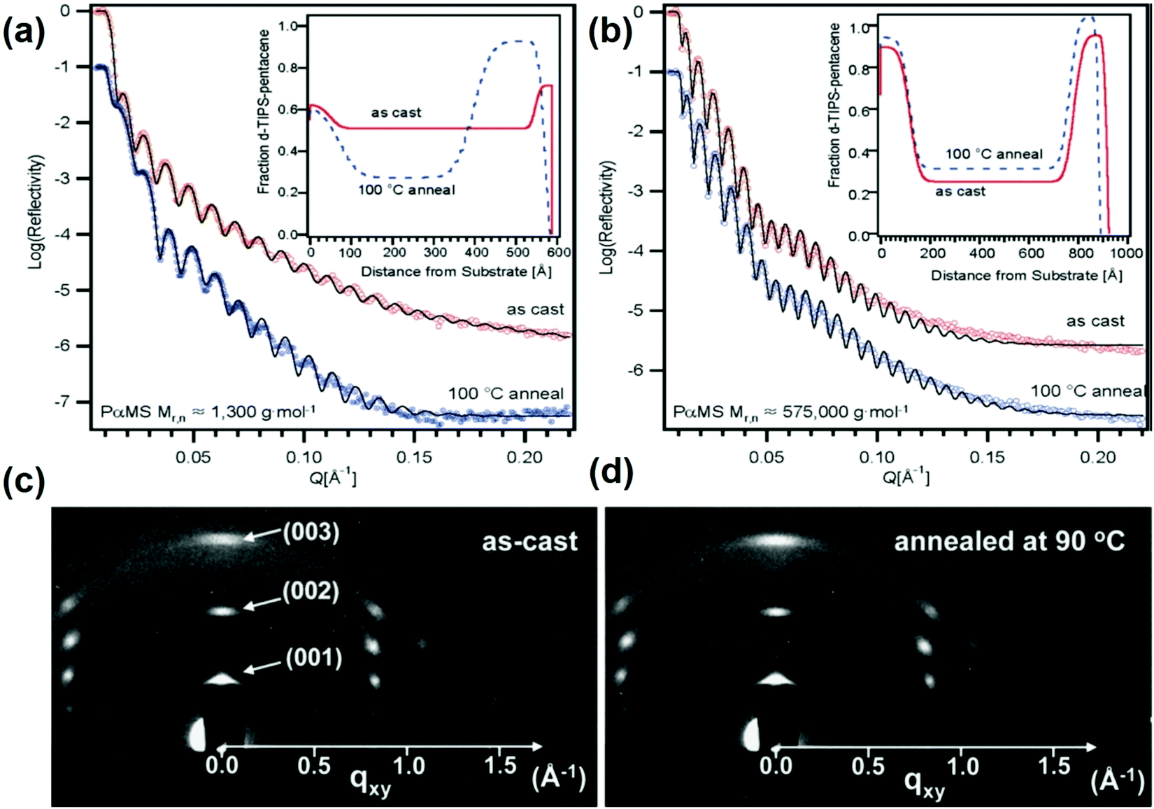 | ||
| Fig. 6 Neutron reflectivity profiles of the TIPS pentacene/PαMS blend film with different PαMS molecular weights of (a) 1.3 K and (b) 575 K, before and after thermal annealing at 100 °C. The insets show the fitted concentration profiles. GIXD patterns of the TIPS pentacene/PαMS blend film with a molecular weight of 575 K, measured (c) after spin coating and (d) after thermal annealing at 90 °C. Reproduced from ref. 197, with permission from American Chemical Society. | ||
3.3 Poly(methyl methacrylate) with varying molecular weights
PMMA is a thermoplastic polymer with optical transparency. PMMA shows outstanding properties such as high impact strength, scratch resistance, and lightweight. The incorporation of an adjacent methyl group in the PMMA structure inhibits close packing and free rotation, which results in an amorphous nature of PMMA.198 PMMA has extensive applications such as in optics, polymer viscosity and biomedical engineering, and also finds important implementation in nanotechnology because of its easy processing and good compatibility with inorganic materials such as carbon nanotubes.199 As one of the most studied polymers for blending with organic semiconductors, PMMA demonstrates exceptional capability for enhancing semiconductor growth,200 film crystallinity,201 grain size,202 phase segregation,203 device air stability195 and charge transport.204 Besides, PMMA also shows excellent gate dielectric properties when employed as the polymer gate insulator material for thin film transistors205,206 and gas sensors.207Kim et al. studied how different molecular weights of PMMA impacted the polymorphism and charge transport of a C8-BTBT organic semiconductor.208 PMMA with different molecular weights including 15 K, 120 K, 350 K, and 996 K were mixed with C8-BTBT before spin coating the blends for crystal growth using a solvent vapor annealing method. As shown in the polarized optical microscopic images in Fig. 7, the crystallization and resultant dimensions of the C8-BTBT rods, in terms of rod height, width and length, were observed to be dependent on the molecular weight of PMMA. In particular, the rod dimension becomes larger as the PMMA molecular weight increases. This was attributed to the reduced polarity of higher molecular weight PMMA, which allowed the free migration of C8-BTBT on the PMMA surface to form enlarged dimensions. Electrical characterization results of C8-BTBT/PMMA (molecular weight 120K) based thin film transistors indicated that the source-drain currents exhibited a tremendous increase by 3–4 orders of magnitude as the device was applied to thermal cycling. This was due to the increased resistivity of C8-BTBT induced by the varying temperatures, at which point the C8-BTBT molecules become oriented downward the substrate. A mobility of 15.6 cm2 V−1 s−1 was obtained when heating was applied to the C8-BTBT/PMMA blend based thin film transistors.
 | ||
| Fig. 7 Polarized optical microscopic images of the crystallization of C8-BTBT rods on PMMA with various molecular weights including (a) 15 K, (b) 120 K, (c) 350 K, and (d) 996 K. Reproduced from ref. 208, with permission from Wiley. | ||
3.4 Polyethylene oxide with varying molecular weights
Polyethylene oxide (PEO) finds important applications in pharmaceutics and is compatible with pharmaceutical dosage due to its thermoplastic behavior. When combined with other polymers, PEO can be utilized to realize controllable drug release.209 In particular, PEO with a high molecular weight is suitable for designing melt-extruded matrices with extended release. On the other hand, PEO is a semicrystalline polymer exhibiting unique crystallization behavior in stark contrast to the conjugated and amorphous counterparts. PEO can eliminate the potential impact of conjugated polymer induced π–π interactions and cocrystallization on the target organic semiconductor,38 which is not a feasible process to optimize for simplified device fabrication procedures. With that said, PEO retains the amorphous nature which helps improve the semiconductor diffusivity and surface energies. The semicrystalline PEO is known for its own crystallization, which is independent of but competing with the crystal growth of the organic semiconductor. These traits of PEO uniquely offer a pathway to modulate solution-based organic semiconductor crystallization from a whole new perspective.He et al. studied the effect of semicrystalline polymer additive PEO with different molecular weights including 8 K and 100 K on the crystallization and charge transport of organic semiconductor TIPS pentacene.210 With the selection of 8K and 100K molecular weights, the PEO polymer with both light and heavy chain entanglements and its impact on modulating semiconductor crystallization can be compared. PEO was mixed with TIPS pentacene at a 1:1 weight ratio before the mixture was deposited to form the active layer via drop casting. Fig. 8(a–d) show the morphology of the TIPS pentacene/PEO (molecular weight of 8 K) crystals based on different sections of the same substrate. The charge transport direction in the organic crystals is highlighted by red arrows. The dark regions observed in Fig. 8 are the formation of PEO crystals, as a result of its own nucleation and crystallization process. The crystal dimensions of PEO crystals are typically under 20 microns, which is consistent with the observation in Fig. 8. In comparison, TIPS pentacene crystals exhibit clear longitudinal dimension extending to a few hundred of microns and also crystal orientation-induced color variations in the crystalline domains under a polarized light microscope. It can be referred that the TIPS pentacene crystals were aligned by the addition of the PEO polymer with a lower molecular weight of 8 K. The effects on modulating the TIPS pentacene crystallization can be attributed to the partially amorphous nature of PEO, which tunes the semiconductor diffusivity and surface energy of faceted evolution.
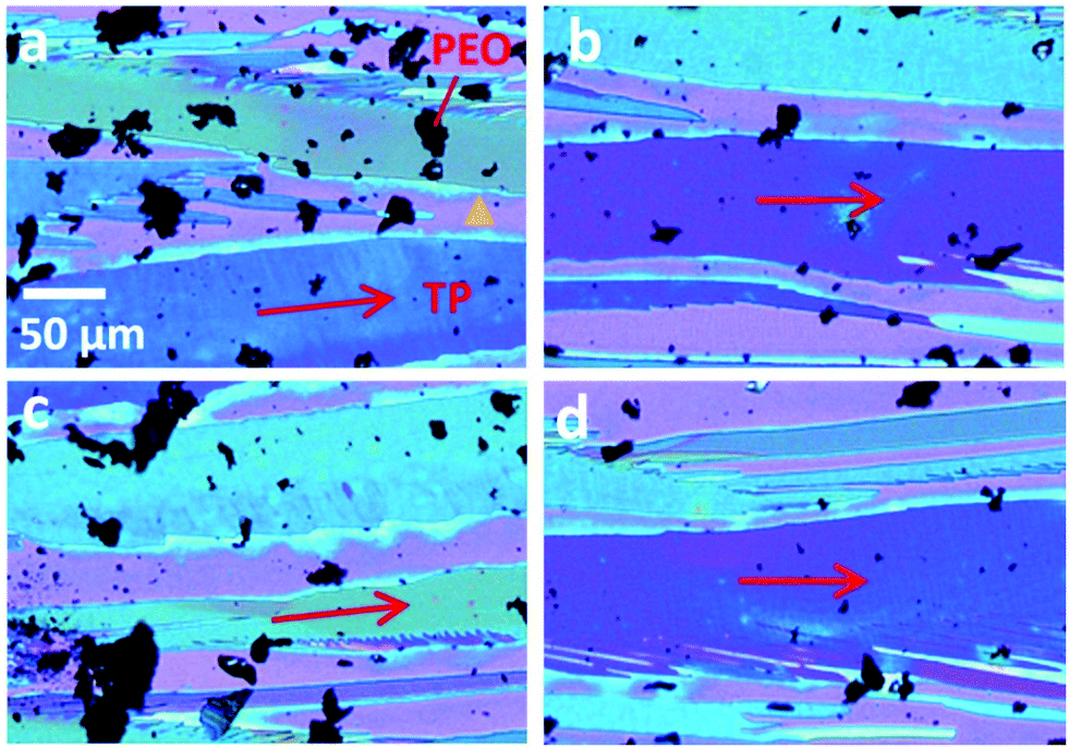 | ||
| Fig. 8 (a–d) Four polarized microscope images of TIPS pentacene crystals with the PEO polymer additive (molecular weight of 8 K). The charge transport direction in the TIPS pentacene/PEO crystals is highlighted by the red arrows. The substrate uncovered by TIPS pentacene/PEO crystals is marked by the yellow triangles. The scale bar shown in (a) applies to all images. Reproduced from ref. 210, with permission from Springer Nature. | ||
In contrast, blending TIPS pentacene with a PEO polymer with a higher molecular weight of 100 K resulted in a distinctively different thin film morphology as shown in the optical images in Fig. 9(a–d). A PEO polymer with a 100 K molecular weight did not benefit TIPS pentacene from reducing random crystal orientations, as indicated by the misoriented red arrows in various directions. Additionally, the film was composed of a top TIPS pentacene/PEO crystal layer as well as a bottom base layer, suggesting strong vertical phase segregation. The blending of PEO with a higher molecular weight likely enhances the interaction between the polymer hydroxyl groups and the silicon dioxide layer on the substrate, further attributing to the phase segregation as observed in the optical images in Fig. 9. Although no obvious crystal alignment was observed, the PEO additive with a molecular weight of 100K showed a more pronounced effect on promoting film formation and increasing coverage. TIPS pentacene/PEO mixture film was further used as the active layer for fabricating bottom-gate, top-contact thin film transistors. The addition of PEO with a lower molecular weight of 8 K resulted in a mobility of 0.017 cm2 V−1 s−1, which is 5-fold larger as compared to that based on PEO with a molecular weight of 100 K.
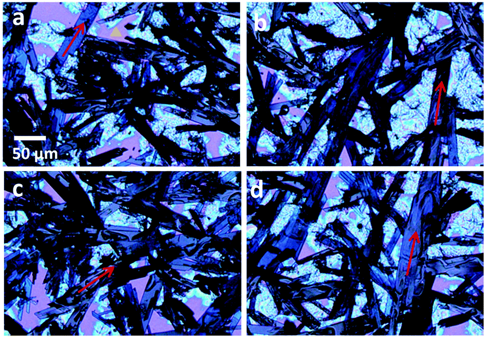 | ||
| Fig. 9 (a-d) Four polarized optical microscope images of TIPS pentacene crystals with the PEO polymer additive (molecular weight of 100 K). The charge transport direction in the TIPS pentacene/PEO crystals is highlighted by the red arrows. The uncovered substrate is marked by the yellow triangle. The scale bar shown in (a) applies to all images. Reproduced from ref. 210, with permission from Springer Nature. | ||
The different studies reviewed in this section are summarized in Table 1, which lists the authors, polymer (with its molecular weight), semiconductor, result and mobility.
| Authors | Polymer | Semiconductor | Result | Mobility |
|---|---|---|---|---|
| Leonardia et al. | PS (3 K, 100 K) | PDPP-TT(1)-SVS(9) | PS resulted in vertical phase segregation and formed a top encapsulation layer; thickness of the top layer depended on PS molecular weight | 0.22 cm2 V−1 s−1 |
| Niazi et al. | PS (2.2 K, 900 K) | diF-TES-ADT | PS molecular weight impacted film morphology, phase segregation and compositions | 6.7 cm2 V−1 s−1 |
| Haase et al. | PS (2 K, 20 K, 200 K, 2000 K) | C8-BTBT | Increase in molecular weight of PS resulted in spherulitic to ribbon-like morphology | 14.4 cm2 V−1 s−1 |
| Singsumphan et al. | PS (13 K, 35 K, 280 K) | TIPS-anthracene | PS of different molecular weights induced different thin film morphologies due to difference in viscosity and processability | Not reported |
| Rocha et al. | PS (2 K, 20 K, 200 K, 2000 K) | TIPS pentacene | Different PS molecular weights impacted intermixing, phase segregation, morphology and charge transport | 12.3 cm2 V−1 s−1 |
| Han et al. | PS (1.3 K, 250 K, 280 K and 290 K) | P3HT | PS with a high molecular weight resulted in a more continuous P3HT microstructure, enhancing gas sensor response | 0.03 cm2 V−1 s−1 |
| Ohe et al. | PαMS (2 K, 20 K, 60 K, 100 K, 800 K) | TIPS pentacene | PαMS with a high molecular weight resulted in a positive Gibbs free energy upon mixing and vertical phase segregation | 0.1 cm2 V−1 s−1 |
| Kang et al. | PαMS (1.3 K and 575 K) | TIPS pentacene | PαMS with a high molecular weight enhanced vertical phase segregation and induced a thicker TIPS pentacene at the charge transport interface | 0.54 cm2 V−1 s−1 |
| Kim et al. | PMMA (15 K, 120 K, 350 K, and 996 K) | C8-BTBT | Crystal dimensions of C8-BTBT increased with molecular weight of PMMA; thermal cycling tunes resistivity and thereby charge transport of C8-BTBT | 15.6 cm2 V−1 s−1 |
| He et al. | PEO (8 K, 100 K) | TIPS pentacene | PEO with 8 K molecular weight improved crystal alignment, whereas PEO with 100 K increased film coverage | 0.017 cm2 V−1 s−1 |
4. Conclusions and outlook
In this article, we have reviewed the influence of polymer additives with different molecular weights on the crystallization, vertical phase separation, compositional structure, thin film morphology and charge carrier mobility of solution-processed organic semiconductors. We first discussed the general benefits of mixing organic semiconductors with amorphous polymers, conjugated polymers, and semicrystalline polymers, respectively. Then, we reviewed several extensively studied amorphous polymers PS, PαMS and PMMA, as well as semicrystalline polymer PEO, in the context of small-molecular organic semiconductors such as TIPS pentacene, C8-BTBT and diF-TES-ADT. In particular, PS with different molecular weights impacted solution viscosity, processability, solute intermixing, phase segregation, crystal morphology and active layer compositions. PαMS with different molecular weights influenced Gibbs free energy upon intermixing, phase segregation, semiconductor layer thickness and charge transport. PMMA with different molecular weights led to different film interconnection, grain boundary, crystal dimension and charge transport. PEO with different molecular weights affected crystal alignment, film coverage, and charge carrier mobility. Using these representative organic semiconductor and polymer additive examples, we demonstrate in this work an easy and useful pathway to manipulate the charge transport of solution-processable organic semiconductors more effectively by tuning the molecular weight of the polymer additive component.While current research is underway in many aspects of organic electronics, we believe future endeavors that focus on these following topics will likely yield exciting discoveries. First, chemical engineering of the polymeric structures is a useful way to tune the molecular weight but at the same time add new properties to the polymers. For instance, side chain engineering can bestow solubility in organic solvents,211,212 regulate molecular packing,213,214 and modulate intermolecular interactions.215,216 Second, polymers with both a similar molecular weight and a similar molecular structure, but with different side chain lengths, present another way to tune molecular stacking,217,218 thin film morphology,219,220 and charge transport.221,222 Third, polymers can be deposited as an additional dielectric layer which helps tune the dielectric properties,223,224 eliminate substrate hydroxyl groups,225 reduce surface roughness,226 enable low-voltage operation,227 enhance film topography,228 control polarizability,229 and improve charge carrier mobility.230,231 Fourth, while current polymer mixing studies are predominately carried out on p-type organic semiconductors, the n-type counterparts are equally important to realize the fabrication of electronic devices such as complementary inverts and logic circuits.232,233 Mixing these polymer additives with n-type organic semiconductors can provide a more effective approach to control semiconductor crystallization, improve electron charge transport, and modulate surface passivation.234,235 Future research in these aforementioned areas may shed light on further improving the overall electronic device performance.
Conflicts of interest
There are no conflicts to declare.Acknowledgements
S. Bi would like to thank Science and Technology Project of Liaoning Province (20180540006).References
- D. Powell, E. V. Campbell, L. Flannery, J. Ogle, S. E. Soss and L. Whittaker-Brooks, Steric hindrance dependence on the spin and morphology properties of highly oriented self-doped organic small molecule thin films, Mater. Adv., 2021, 2(1), 356–365 RSC.
- M. Reali, P. Saini and C. Santato, Electronic and protonic transport in bio-sourced materials: a new perspective on semiconductivity, Mater. Adv., 2021, 2(1), 15–31 RSC.
- Q. Wang, S. Jiang, Y. Shi and Y. Li, Effect of access resistance on the experimentally measured temperature–carrier mobility dependence in highly-crystalline DNTT-based transistors, Mater. Adv., 2020, 1(6), 1799–1804 RSC.
- S. Bi, Q. Li, Y. Yan, K. Asare-Yeboah, T. Ma, C. Tang, Z. Ouyang, Z. He, Y. Liu and C. Jiang, Layer-dependent anisotropic frictional behavior in two-dimensional monolayer hybrid perovskite/ITO layered heterojunctions, Phys. Chem. Chem. Phys., 2019, 21(5), 2540–2546 RSC.
- J.-H. Tang and Y. Sun, Visible-light-driven organic transformations integrated with H2 production on semiconductors, Mater. Adv., 2020, 1(7), 2155–2162 RSC.
- J. H. L. Ngai, C. C. M. Chan, C. H. Y. Ho, J. K. W. Ho, S. H. Cheung, H. Yin and S. K. So, A facile and robust approach to prepare fluorinated polymer dielectrics for probing the intrinsic transport behavior of organic semiconductors, Mater. Adv., 2020, 1(4), 891–898 RSC.
- Q. Liu, Y. Wang, L. Arunagiri, M. Khatib, S. Manzhos, K. Feron, S. E. Bottle, H. Haick, H. Yan, T. Michinobu and P. Sonar, Versatile nature of anthanthrone based polymers as active multifunctional semiconductors for various organic electronic devices, Mater. Adv., 2020, 1(9), 3428–3438 RSC.
- S. Bi, W. Zhao, Y. Sun, C. Jiang, Y. Liu, Z. He, Q. Li and J. Song, Dynamic photonic perovskite light-emitting diodes with post-treatment-enhanced crystallization as writable and wipeable inscribers, Nanoscale Adv., 2021, 3(23), 6659–6668 RSC.
- J. Guo, B. Yu, F. Zhu and D. Yan, Significant improvement of 2,9-DPh-DNTT organic thin-film transistors based on organic heterojunction buffer layer, Org. Electron., 2021, 93, 106159 CrossRef CAS.
- W. Li, L. Li, Q. Sun, X. Liu, M. Kanehara, T. Nakayama, J. Jiu, K. Sakamoto and T. Minari, Direct fabrication of high-resolution and high-performance flexible electronics via surface-activation-localized electroless plating, Chem. Eng. J., 2021, 416, 127644 CrossRef CAS.
- K. J. Thorley, M. Benford, Y. Song, S. R. Parkin, C. Risko and J. E. Anthony, What is special about silicon in functionalised organic semiconductors?, Mater. Adv., 2021, 2(16), 5415–5421 RSC.
- Z. He, Z. Zhang and S. Bi, Nanoparticles for organic electronics applications, Mater. Res. Express, 2020, 7, 012004 CrossRef CAS.
- Z. Yang, S. Lin, J. Liu, K. Zheng, G. Lu, B. Ye, J. Huang, Y. Zhang, Y. Ye, T. Guo and G. Chen, High performance phototransistors with organic/quantum dot composite materials channels, Org. Electron., 2020, 78, 105565 CrossRef CAS.
- J. H. Chen, J. Anthony and D. C. Martin, Thermally induced solid-state phase transition of bis(triisopropylsilylethynyl) pentacene crystals, J. Phys. Chem. B, 2006, 110(33), 16397–16403 CrossRef CAS PubMed.
- D. Kneppe, F. Talnack, B. K. Boroujeni, C. Teixeira da Rocha, M. Höppner, A. Tahn, S. C. B. Mannsfeld, F. Ellinger, K. Leo and H. Kleemann, Solution-processed pseudo-vertical organic transistors based on TIPS-pentacene, Mater. Today Energy, 2021, 21, 100697 CrossRef CAS.
- Z. He, Z. Zhang, S. Bi, K. Asare-Yeboah, J. Chen and D. Li, A facile and novel route to improve TIPS pentacene based organic thin film transistor performance with elastomer, Synth. Met., 2020, 262, 116337 CrossRef CAS.
- J. H. Chen, J. E. Anthony and D. C. Martin, Crystallographic cracking during a thermally-induced solid-state phase transition in TIPS pentacene, Abstr. Pap. Am. Chem. Soc., 2005, 230, 309 Search PubMed.
- G. Schweicher, G. Liu, P. Fastré, R. Resel, M. Abbas, G. Wantz and Y. H. Geerts, Directional crystallization of C8-BTBT-C8 thin films in a temperature gradient, Mater. Chem. Front., 2021, 5(1), 249–258 RSC.
- R. Janneck, T. S. Nowack, F. De Roose, H. Ali, W. Dehaene, P. Heremans, J. Genoe and C. Rolin, Integration of highly crystalline C8-BTBT thin-films into simple logic gates and circuits, Org. Electron., 2019, 67, 64–71 CrossRef CAS.
- W. Zhao, J. Jie, Q. Wei, Z. Lu, R. Jia, W. Deng, X. Zhang and X. Zhang, A facile method for the growth of organic semiconductor single crystal arrays on polymer dielectric toward flexible field-effect transistors, Adv. Funct. Mater., 2019, 29(32), 1902494 CrossRef.
- Z. Chai, S. A. Abbasi and A. A. Busnaina, Scalable directed assembly of highly crystalline 2,7-dioctyl[1]benzothieno[3,2-b][1]benzothiophene (C8-BTBT) films, ACS Appl. Mater. Interfaces, 2018, 10(21), 18123–18130 CrossRef CAS PubMed.
- S. Bi, Y. Li, Z. He, Z. Ouyang, Q. Guo and C. Jiang, Self-assembly diketopyrrolopyrrole-based materials and polymer blend with enhanced crystal alignment and property for organic field-effect transistors, Org. Electron., 2019, 65, 96–99 CrossRef CAS.
- S. Y. Qu and H. Tian, Diketopyrrolopyrrole (DPP)-based materials for organic photovoltaics, Chem. Commun., 2012, 48(25), 3039–3051 RSC.
- Y. Qiao, Y. Guo, C. Yu, F. Zhang, W. Xu, Y. Liu and D. Zhu, Diketopyrrolopyrrole-containing quinoidal small molecules for high-performance, air-stable, and solution-processable n-channel organic field-effect transistors, J. Am. Chem. Soc., 2012, 134(9), 4084–4087 CrossRef CAS PubMed.
- Z. Zhang, Z. He, S. Bi and K. Asare-Yeboah, Phase segregation controlled semiconductor crystallization for organic thin film transistors, J. Sci.: Adv. Mater. Devices, 2020, 5(2), 151–163 Search PubMed.
- C.-H. Kim, Bias-stress effects in diF-TES-ADT field-effect transistors, Solid-State Electron., 2019, 153, 23–26 CrossRef CAS.
- S. Hunter, J. H. Chen and T. D. Anthopoulos, Microstructural control of charge transport in organic blend thin-film transistors, Adv. Funct. Mater., 2014, 24(38), 5969–5976 CrossRef CAS.
- J. Panidi, A. F. Paterson, D. Khim, Z. P. Fei, Y. Han, L. Tsetseris, G. Vourlias, P. A. Patsalas, M. Heeney and T. D. Anthopoulos, Remarkable enhancement of the hole mobility in several organic small-molecules, polymers, and small-molecule:polymer blend transistors by simple admixing of the Lewis acid p-dopant B(C6F5)(3), Adv. Sci., 2018, 5(1), 1700290 CrossRef PubMed.
- K. N. Choi, K. S. Kim, K. S. Chung and H. Lee, Solvent Effect on the Electrical Properties of Triisopropylsilylethynyl (TIPS) Pentacene Organic Thin-Film Transistors, IEEE Trans. Device Mater. Reliab., 2009, 9(3), 489–493 CAS.
- Z. He, Z. Zhang, K. Asare-Yeboah and S. Bi, Poly(α-methylstyrene) polymer and small-molecule semiconductor blend with reduced crystal misorientation for organic thin film transistors, J. Mater. Sci.: Mater. Electron., 2019, 30, 14335–14343 CrossRef CAS.
- J. H. Chen, D. C. Martin and J. E. Anthony, Morphology and molecular orientation of thin-film bis(triisopropylsilylethynyl) pentacene, J. Mater. Res., 2007, 22(6), 1701–1709 CrossRef CAS.
- W. Zhou, N. J. Yutronkie, B. H. Lessard and J. L. Brusso, From chemical curiosity to versatile building blocks: Unmasking the hidden potential of main-group phthalocyanines in organic field-effect transistors, Mater. Adv., 2021, 2(1), 165–185 RSC.
- S. Sehlangia, S. Sharma, S. K. Sharma and C. P. Pradeep, 2,2′-(Arylenedivinylene)bis-8-hydroxyquinolines exhibiting aromatic π–π stacking interactions as solution-processable p-type organic semiconductors for high-performance organic field effect transistors, Mater. Adv., 2021, 2(14), 4643–4651 RSC.
- T. Hodsden, K. J. Thorley, A. Basu, A. J. P. White, C. Wang, W. Mitchell, F. Glöcklhofer, T. D. Anthopoulos and M. Heeney, The influence of alkyl group regiochemistry and backbone fluorination on the packing and transistor performance of N-cyanoimine functionalised indacenodithiophenes, Mater. Adv., 2021, 2(5), 1706–1714 RSC.
- A. R. Kirmani, E. F. Roe, C. M. Stafford and L. J. Richter, Role of the electronically-active amorphous state in low-temperature processed In2O3 thin-film transistors, Mater. Adv., 2020, 1(2), 167–176 RSC.
- A. Rianjanu, R. Aflaha, N. I. Khamidy, M. Djamal, K. Triyana and H. S. Wasisto, Room-temperature ppb-level trimethylamine gas sensors functionalized with citric acid-doped polyvinyl acetate nanofibrous mats, Mater. Adv., 2021, 2(11), 3705–3714 RSC.
- R. Malik, N. Joshi and V. K. Tomer, Advances in the designs and mechanisms of MoO3 nanostructures for gas sensors: A holistic review, Mater. Adv., 2021, 2(13), 4190–4227 RSC.
- J. M. Suh, T. H. Eom, S. H. Cho, T. Kim and H. W. Jang, Light-activated gas sensing: A perspective of integration with micro-LEDs and plasmonic nanoparticles, Mater. Adv., 2021, 2(3), 827–844 RSC.
- K. Asare-Yeboah, Q. Li, C. Jiang, Z. He, S. Bi, Y. Liu and C. Liu, High performance and efficiency resonant photo-effect-transistor by near-field nano-strip-controlled organic light emitting diode gate, J. Phys. Chem. Lett., 2020, 11(16), 6526–6534 CrossRef CAS PubMed.
- S. Bi, Q. Li, Z. He, Q. Guo, K. Asare-Yeboah, Y. Liu and C. Jiang, Highly enhanced performance of integrated piezo photo-transistor with dual inverted OLED gate and nanowire array channel, Nano Energy, 2019, 66, 104101 CrossRef CAS.
- J. Panidi, J. Kainth, A. F. Paterson, S. Wang, L. Tsetseris, A.-H. Emwas, M. A. McLachlan, M. Heeney and T. D. Anthopoulos, Introducing a nonvolatile N-type dopant drastically improves electron transport in polymer and small-molecule organic transistors, Adv. Funct. Mater., 2019, 29(34), 1902784 CrossRef.
- D. Panigrahi, R. Hayakawa, K. Honma, K. Kanai and Y. Wakayama, Organic heterojunction transistors for mechanically flexible multivalued logic circuits, Appl. Phys. Express, 2021, 14(8), 081004 CrossRef CAS.
- Z. Yang, S. Lin, J. Liu, K. Zheng, G. Lu, B. Ye, J. Huang, Y. Zhang, Y. Ye, T. Guo and G. Chen, Integration of highly crystalline C8-BTBT thin-films into simple logic gates and circuits, Org. Electron., 2020, 78, 64–71 Search PubMed.
- Q. Li, C. Jiang, S. Bi, K. Asare-Yeboah, Z. He and Y. Liu, Photo-triggered logic circuits assembled on integrated illuminants and resonant nanowires, ACS Appl. Mater. Interfaces, 2020, 12(24), 46501–46508 CrossRef CAS PubMed.
- C. Pitsalidis, N. Kalfagiannis, N. A. Hastas, P. G. Karagiannidis, C. Kapnopoulos, A. Ioakeimidis and S. Logothetidis, High performance transistors based on the controlled growth of triisopropylsilylethynyl-pentacene crystals via non-isotropic solvent evaporation, RSC Adv., 2014, 4(40), 20804–20813 RSC.
- X. Wang, M. Yuan, X. Xiong, M. Chen, M. Qin, L. Qiu, H. Lu, G. Zhang, G. Lv and A. H. W. Choi, Process optimization for inkjet printing of triisopropylsilylethynyl pentacene with single-solvent solutions, Thin Solid Films, 2015, 578, 11–19 CrossRef CAS.
- Z. He, Z. Zhang, S. Bi, K. Asare-Yeboah and J. Chen, Ultra-low misorientation angle in small-molecule semiconductor/polyethylene oxide blends for organic thin film transistors, J. Polym. Res., 2020, 27(3), 75 CrossRef CAS.
- Y.-H. Kim, Y. U. Lee, J.-I. Han, S.-M. Han and M.-K. Han, Influence of solvent on the film morphology, crystallinity and electrical characteristics of triisopropylsilyl pentacene OTFTs, J. Electrochem. Soc., 2007, 154(12), H995–H998 CrossRef CAS.
- D. K. Hwang, C. Fuentes-Hernandez, J. D. Berrigan, Y. N. Fang, J. Kim, W. J. Potscavage, H. Cheun, K. H. Sandhage and B. Kippelen, Solvent and polymer matrix effects on TIPS-pentacene/polymer blend organic field-effect transistors, J. Mater. Chem., 2012, 22(12), 5531–5537 RSC.
- M. S. Ozorio, S. A. Camacho, N. J. A. Cordeiro, J. P. L. Duarte and N. Alves, Solvent effect on morphology and optical properties of poly(3-hexylthiophene): TIPS-pentacene blends, J. Electron. Mater., 2018, 47(2), 1353–1361 CrossRef CAS.
- M. Chen, B. Peng, S. Huang and P. K. L. Chan, Understanding the meniscus-guided coating parameters in organic field-effect-transistor fabrications, Adv. Funct. Mater., 2020, 30(1), 1905963 CrossRef CAS.
- M. Kondo, T. Kajitani, T. Uemura, Y. Noda, F. Ishiwari, Y. Shoji, T. Araki, S. Yoshimoto, T. Fukushima and T. Sekitani, Highly-ordered triptycene modifier layer based on blade coating for ultraflexible organic transistors, Sci. Rep., 2019, 9(1), 9200 CrossRef PubMed.
- D. Wu, M. Kaplan, H. W. Ro, S. Engmann, D. A. Fischer, D. M. DeLongchamp, L. J. Richter, E. Gann, L. Thomsen, C. R. McNeill and X. Zhang, Blade coating aligned, high-performance, semiconducting-polymer transistors, Chem. Mater., 2018, 30(6), 1924–1936 CrossRef CAS.
- L. Ding, J. Zhao, Y. Huang, W. Tang, S. Chen and X. Guo, Flexible-blade coating of small molecule organic semiconductor for low voltage organic field effect transistor, IEEE Electron Device Lett., 2017, 38(3), 338–340 CAS.
- R. Hofmockel, U. Zschieschang, U. Kraft, R. Rödel, N. H. Hansen, M. Stolte, F. Würthner, K. Takimiya, K. Kern, J. Pflaum and H. Klauk, High-mobility organic thin-film transistors based on a small-molecule semiconductor deposited in vacuum and by solution shearing, Org. Electron., 2013, 14(12), 3213–3221 CrossRef CAS.
- S. Galindo, A. Tamayo, F. Leonardi and M. Mas-Torrent, Control of polymorphism and morphology in solution sheared organic field-effect transistors, Adv. Funct. Mater., 2017, 27(25), 1700526 CrossRef.
- Q. Meng, F. Zhang, Y. Zang, D. Huang, Y. Zou, J. Liu, G. Zhao, Z. Wang, D. Ji, C.-A. Di, W. Hu and D. Zhu, Solution-sheared ultrathin films for highly-sensitive ammonia detection using organic thin-film transistors, J. Mater. Chem. C, 2014, 2(7), 1264–1269 RSC.
- Z. Liu, H. A. Becerril, M. E. Roberts, Y. Nishi and Z. Bao, Experimental study and statistical analysis of solution-shearing processed organic transistors based on an asymmetric small-molecule semiconductor, IEEE Trans. Electron Devices, 2009, 56(2), 176–185 CAS.
- M. Stolte, M. Gsänger, R. Hofmockel, S.-L. Suraru and F. Würthner, Improved ambient operation of n-channel organic transistors of solution-sheared naphthalene diimide under bias stress, Phys. Chem. Chem. Phys., 2012, 14(41), 14181–14185 RSC.
- S. Huang, B. Peng and P. K. L. Chan, Ambipolar organic field-effect transistors based on a dual-function, ultrathin and highly crystalline 2,9-didecyldinaphtho[2,3-b:2′,3′-f]thieno[3,2-b]thiophene (C10-DNTT) layer, Adv. Electron. Mater., 2017, 3(12), 1700268 CrossRef.
- K. Kim, K. Nam, X. Li, D. Y. Lee and S. H. Kim, Programmed design of highly crystalline organic semiconductor patterns with uniaxial alignment via blade coating for high-performance organic field-effect, ACS Appl. Mater. Interfaces, 2019, 11(45), 42403–42411 CrossRef CAS PubMed.
- B. Y. Peng, S. Y. Huang, Z. W. Zhou and P. K. L. Chan, Solution-processed monolayer organic crystals for high-performance field-effect transistors and ultrasensitive gas sensors, Adv. Funct. Mater., 2017, 27(29), 1700999 CrossRef.
- A. Bilgaiyan, S.-I. Cho, M. Abiko, K. Watanabe and M. Mizukami, Flexible, high mobility short-channel organic thin film transistors and logic circuits based on 4H-21DNTT, Sci. Rep., 2021, 11(1), 11710 CrossRef CAS PubMed.
- Y. Y. Zhao, X. Y. Fan, J. G. Feng, X. D. Wang, Y. C. Wu, B. Su and L. Jiang, Regulated dewetting for patterning organic single crystals with pure crystallographic orientation toward high performance field-effect transistors, Adv. Funct. Mater., 2018, 28(49), 1800470 CrossRef.
- T. Shen, H. Zhou, X. Liu, Y. Fan, D. D. Mishra, Q. Fan, Z. Yang, X. Wang, M. Zhang and J. Li, Wettability Control of Interfaces for High-Performance Organic Thin-Film Transistors by Soluble Insulating Polymer Films, ACS Omega, 2020, 5(19), 10891–10899 CrossRef CAS PubMed.
- X. Z. Wei Deng, H. Dong, J. Jie, X. Xu, J. Liu, L. He, L. Xu, W. Hu and X. Zhang, Channel-restricted meniscus self-assembly for uniformly aligned growth of single-crystal arrays of organic semiconductors, Mater. Today, 2019, 24, 17–25 CrossRef.
- J. Chang, C. Chi, J. Zhang and J. Wu, Controlled growth of large-area high-performance small-molecule organic single-crystalline transistors by slot-die coating using a mixed solvent system, Adv. Mater., 2013, 25(44), 6442–6447 CrossRef CAS PubMed.
- R. Wang, H.-j. Kwon, X. Tang, H. Ye, C. E. Park, J. Kim, H. Kong and S. H. Kim, Slot-die coating of sol–gel-based organic–inorganic nanohybrid dielectric layers for flexible and large-area organic thin film transistors, Appl. Surf. Sci., 2020, 529, 147198 CrossRef CAS.
- J. Chang, Z. Lin, J. Li, S. L. Lim, F. Wang, G. Li, J. Zhang and J. Wu, Enhanced polymer thin film transistor performance by carefully controlling the solution self-assembly and film alignment with slot die coating, Adv. Electron. Mater., 2015, 1(7), 1500036 CrossRef.
- A. K. K. Kyaw, L. S. Lay, G. W. Peng, J. Changyun and Z. Jie, A nanogroove-guided slot-die coating technique for highly ordered polymer films and high-mobility transistors, Chem. Commun., 2016, 52(2), 358–361 RSC.
- Z. Lin, X. Guo, L. Zhou, C. Zhang, J. Chang, J. Wu and J. Zhang, Solution-processed high performance organic thin film transistors enabled by roll-to-roll slot die coating technique, Org. Electron., 2018, 54, 80–88 CrossRef CAS.
- P. Xie, T. Liu, J. Sun, J. Jiang, Y. Yuan, Y. Gao, J. Zhou and J. Yang, Solution-processed ultra-flexible C8-BTBT organic thin-film transistors with the corrected mobility over 18 cm2/(V s), Sci. Bull., 2020, 65(10), 791–795 CrossRef CAS.
- W. Han and Z. Q. Lin, Learning from “Coffee Rings”: Ordered structures enabled by controlled evaporative self-assembly, Angew. Chem., Int. Ed., 2012, 51(7), 1534–1546 CrossRef CAS PubMed.
- A. J. Petsi and V. N. Burganos, Evaporation-induced flow in an inviscid liquid line at any contact angle, Physical Review E, 2006, 73(4), 041201 CrossRef CAS PubMed.
- H. S. Lee, D. Kwak, W. H. Lee, J. H. Cho and K. Cho, Self-organization characteristics of soluble pentacene on wettability-controlled patterned substrate for organic field-effect transistors, J. Phys. Chem. C, 2010, 114(5), 2329–2333 CrossRef CAS.
- Z. Wang, H. Guo, J. Li, L. Wang and G. Dong, Marangoni effect-controlled growth of oriented film for high performance C8-BTBT transistors, Adv. Mater. Interfaces, 2019, 6(8), 1801736 CrossRef.
- J. Soeda, T. Uemura, T. Okamoto, C. Mitsui, M. Yamagishi and J. Takeya, Inch-size solution-processed single-crystalline films of high-mobility organic semiconductors, Appl. Phys. Express, 2013, 6(7), 076503 CrossRef.
- K. Manoli, L. M. Dumitru, M. Y. Mulla, M. Magliulo, C. D. Franco, M. V. Santacroce, G. Scamarcio and L. Torsi, A comparative study of the gas sensing behavior in P3HT- and PBTTT-based OTFTs: The influence of film morphology and contact electrode position, Sensors, 2014, 14(9), 16869–16880 CrossRef PubMed.
- Y. Seo, J. H. Lee, J. E. Anthony, K. V. Nguyen, Y. H. Kim, H. W. Jang, S. Ko, Y. Cho and W. H. Lee, Effects of grain boundary density on the gas sensing properties of triethylsilylethynyl-anthradithiophene field-effect transistors, Adv. Mater. Interfaces, 2018, 5(3), 1701399 CrossRef.
- S. Hou, X. Zhuang, H. Fan and J. Yu, Grain boundary control of organic semiconductors via solvent vapor annealing for high-sensitivity NO2 detection, Sensors, 2021, 21(1), 226 CrossRef CAS PubMed.
- B. Shao, Y. Liu, X. Zhuang, S. Hou, S. Han, X. Yu and J. Yu, Crystallinity and grain boundary control of TIPS-pentacene in organic thin-film transistors for the ultra-high sensitive detection of NO2, J. Mater. Chem. C, 2019, 7(33), 10196–10202 RSC.
- Z. He, Z. Zhang, K. Asare-Yeboah, S. Bi, J. Chen and D. Li, Polyferrocenylsilane semicrystalline polymer additive for solution-processed p-channel organic thin film transistors, Polymers, 2021, 13(3), 402 CrossRef CAS PubMed.
- C. W. Sele, B. K. C. Kjellander, B. Niesen, M. J. Thornton, J. van der Putten, K. Myny, H. J. Wondergem, A. Moser, R. Resel, A. van Breemen, N. van Aerle, P. Heremans, J. E. Anthony and G. H. Gelinck, Controlled deposition of highly ordered soluble acene thin films: Effect of morphology and crystal orientation on transistor performance, Adv. Mater., 2009, 21(48), 4926–4931 CrossRef CAS PubMed.
- S. Yamazaki, T. Hamada, T. Nagase, S. Tokai, M. Yoshikawa, T. Kobayashi, Y. Michiwaki, S. Watase, M. Watanabe, K. Matsukawa and H. Naito, Drastic improvement in wettability of 6,13-bis(triisopropylsilylethynyl)pentacene by addition of silica nanoparticles for solution-processable organic field-effect transistors, Appl. Phys. Express, 2010, 3(9), 091602 CrossRef.
- J. A. Lim, H. S. Lee, W. H. Lee and K. Cho, Control of the morphology and structural development of solution-processed functionalized acenes for high-performance organic transistors, Adv. Funct. Mater., 2009, 19(10), 1515–1525 CrossRef CAS.
- S. S. Lee, C. S. Kim, E. D. Gomez, B. Purushothaman, M. F. Toney, C. Wang, A. Hexemer, J. E. Anthony and Y.-L. Loo, Controlling nucleation and crystallization in solution-processed organic semiconductors for thin-film transistors, Adv. Mater., 2009, 21(35), 3605–3609 CrossRef CAS.
- Z. He, K. Xiao, W. Durant, D. K. Hensley, J. E. Anthony, K. Hong, S. M. Kilbey, II, J. Chen and D. Li, Enhanced performance consistency in nanoparticle/tips pentacene-based organic thin film transistors, Adv. Funct. Mater., 2011, 21(19), 3617–3623 CrossRef CAS.
- D.-K. Kim, P. Vincent, J. Jang, I. M. Kang, H. Kim, P. Lang, M. Choi and J.-H. Bae, Contact line curvature-induced molecular misorientation of a surface energy patterned organic semiconductor in meniscus-guided coating, Appl. Surf. Sci., 2020, 504, 144362 CrossRef CAS.
- J. Chen, M. Shao, K. Xiao, Z. He, D. Li, B. S. Lokitz, D. K. Hensley, S. M. Kilbey, II, J. E. Anthony, J. K. Keum, A. J. Rondinone, W.-Y. Lee, S. Hong and Z. Bao, Conjugated polymer-mediated polymorphism of a high performance, small-molecule organic semiconductor with tuned intermolecular interactions, enhanced long-range order, and charge transport, Chem. Mater., 2013, 25(21), 4378–4386 CrossRef CAS.
- S. C. B. Mannsfeld, M. L. Tang and Z. Bao, Thin film structure of triisopropylsilylethynyl-functionalized pentacene and tetraceno[2,3-b]thiophene from grazing incidence X-ray diffraction, Adv. Mater., 2011, 23(1), 127–131 CrossRef CAS PubMed.
- Z. He, Z. Zhang and S. Bi, Nanoscale alignment of semiconductor crystals for high-fidelity organic electronics applications, Appl. Nanosci., 2021, 11, 787–795 CrossRef CAS.
- H. Yoo, H. H. Choi, T. J. Shin, T. Rim, K. Cho, S. Jung and J.-J. Kim, Self-assembled, millimeter-sized TIPS-pentacene spherulites grown on partially crosslinked polymer gate dielectric, Adv. Funct. Mater., 2015, 25(24), 3658–3665 CrossRef CAS.
- Z. He, Z. Zhang, S. Bi and J. Chen, Tuning charge transport in organic semiconductors with nanoparticles and hexamethyldisilazane, J. Nanopart. Res., 2021, 23(1), 5 CrossRef CAS.
- J. Rivnay, L. H. Jimison, J. E. Northrup, M. F. Toney, R. Noriega, S. Lu, T. J. Marks, A. Facchetti and A. Salleo, Large modulation of carrier transport by grain-boundary molecular packing and microstructure in organic thin films, Nat. Mater., 2009, 8(12), 952–958 CrossRef CAS PubMed.
- Z. He, Z. Zhang and S. Bi, Long-range crystal alignment with polymer additive for organic thin film transistors, J. Polym. Res., 2019, 26(7), 173 CrossRef.
- D. Choi, B. Ahn, S. H. Kim, K. Hong, M. Ree and C. E. Park, High-performance triisopropylsilylethynyl pentacene transistors via spin coating with a crystallization-assisting layer, ACS Appl. Mater. Interfaces, 2012, 4(1), 117–122 CrossRef CAS PubMed.
- Z. He, J. Chen, J. K. Keum, G. Szulczewski and D. Li, Improving performance of TIPS pentacene-based organic thin film transistors with small-molecule additives, Org. Electron., 2014, 15(1), 150–155 CrossRef CAS.
- R. Jia, X. Wu, W. Deng, X. Zhang, L. Huang, K. Niu, L. Chi and J. Jie, Unraveling the mechanism of the persistent photoconductivity in organic phototransistors, Adv. Funct. Mater., 2019, 29(45), 1905657 CrossRef CAS.
- J. H. Chen, C. K. Tee, M. Shtein, D. C. Martin and J. Anthony, Controlled solution deposition and systematic study of charge-transport anisotropy in single crystal and single-crystal textured TIPS pentacene thin films, Org. Electron., 2009, 10(4), 696–703 CrossRef CAS.
- Z. He, N. Lopez, X. Chi and D. Li, Solution-based 5,6,11,12-tetrachlorotetracene crystal growth for high-performance organic thin film transistors, Org. Electron., 2015, 22, 191–196 CrossRef CAS.
- S. Bi, Z. He, J. Chen and D. Li, Solution-grown small-molecule organic semiconductor with enhanced crystal alignment and areal coverage for organic thin film transistors, AIP Adv., 2015, 5(7), 077170 CrossRef.
- J. H. Chen, C. K. Tee, J. Y. Yang, C. Shaw, M. Shtein, J. Anthony and D. C. Martin, Thermal and mechanical cracking in bis(triisopropylsilyiethnyl) pentacene thin films, J. Polym. Sci. Pol. Phys., 2006, 44(24), 3631–3641 CrossRef CAS.
- K. Asare-Yeboah, R. M. Frazier, G. Szulczewski and D. Li, Temperature gradient approach to grow large, preferentially oriented 6,13-bis(triisopropylsilylethynyl) pentacene crystals for organic thin film transistors, J. Vac. Sci. Technol. B, 2014, 32(5), 052401 CrossRef.
- M. Y. Cho, Y. D. Han, H. S. Kang, K. Kim, K. H. Kim, M. J. Cho, D. H. Choi and J. Joo, Photoresponsive characteristics and hysteresis of soluble 6,13-bis(triisopropyl-silylethynyl)-pentacene-based organic thin film transistors with and without annealing, J. Appl. Phys., 2010, 107(3), 6 CrossRef.
- Z. He, J. Chen and D. Li, Crystal alignment for high performance organic electronics devices, J. Vac. Sci. Technol. A, 2019, 37(4), 040801 CrossRef.
- M. J. Lee, D. Gupta, N. Zhao, M. Heeney, I. McCulloch and H. Sirringhaus, Anisotropy of charge transport in a uniaxially aligned and chain-extended, high-mobility, conjugated polymer semiconductor, Adv. Funct. Mater., 2011, 21(5), 932–940 CrossRef CAS.
- Z. He, J. Chen, Z. Sun, G. Szulczewski and D. Li, Air-flow navigated crystal growth for TIPS pentacene-based organic thin-film transistors, Org. Electron., 2012, 13(10), 1819–1826 CrossRef CAS.
- M. J. Kim, H. W. Heo, Y. K. Suh and C. K. Song, Morphology control of TIPS-pentacene grains with inert gas injection and effects on the performance of OTFTs, Org. Electron., 2011, 12(7), 1170–1176 CrossRef CAS.
- L. Yu, X. Li, J. Smith, S. Tierney, R. Sweeney, B. K. C. Kjellander, G. H. Gelinck, T. D. Anthopoulos and N. Stingelin, Solution-processed small molecule transistors with low operating voltages and high grain-boundary anisotropy, J. Mater. Chem., 2012, 22(19), 9458–9461 RSC.
- K. V. Nguyen, M. M. Payne, J. E. Anthony, J. H. Lee, E. Song, B. Kang, K. Cho and W. H. Lee, Grain boundary induced bias instability in soluble acene-based thin-film transistors, Sci. Rep., 2016, 6(1), 33224 CrossRef CAS PubMed.
- Z. He, K. Asare-Yeboah, Z. Zhang and S. Bi, Self-assembly crystal microribbons with nucleation additive for high-performance organic thin film transistors, Jpn. J. Appl. Phys., 2019, 58, 061009 CrossRef CAS.
- X. Meng, Z. Liu, B. Cui, D. Qin, H. Geng, W. Cai, L. Fu, J. He, Z. Ren and J. Sui, Grain boundary engineering for achieving high thermoelectric performance in n-type Skutterudites, Adv. Energy Mater., 2017, 1602582 CrossRef.
- Z. He, Z. Zhang, K. Asare-Yeboah, S. Bi, J. Chen and D. Li, Crystal growth of small-molecule organic semiconductors with nucleation additive, Curr. Appl. Phys., 2021, 21, 107–115 CrossRef.
- Y. Sun, Z. Zhang, K. Asare-Yeboah, S. Bi and Z. He, Poly(butyl acrylate) polymer enhanced phase segregation and morphology of organic semiconductor for solution-processed thin film transistors, J. Appl. Polym. Sci., 2021, 138(27), 50654 CrossRef CAS.
- Z. R. He, J. H. Chen, J. K. Keum, G. Szulczewski and D. W. Li, Improving performance of TIPS pentacene-based organic thin film transistors with small-molecule additives, Org. Electron., 2014, 15(1), 150–155 CrossRef CAS.
- S. H. Jin, K. D. Jung, H. Shin, B.-G. Park and J. D. Lee, Grain size effects on contact resistance of top-contact pentacene TFTs, Synth. Met., 2006, 156(2), 196–201 CrossRef CAS.
- Z. He, Z. Zhang and S. Bi, Small-molecule additives for organic thin film transistors, J. Mater. Sci.: Mater. Electron., 2019, 30, 20899–20913 CrossRef CAS.
- J. Zhang, J. P. Rabe and N. Koch, Grain-boundary evolution in a pentacene monolayer, Adv. Mater., 2008, 20(17), 3254–3257 CrossRef CAS.
- M. Hirose, E. Tsunemi, K. Kobayashi and H. Yamada, Influence of grain boundary on electrical properties of organic crystalline grains investigated by dual-probe atomic force microscopy, Appl. Phys. Lett., 2013, 103(17), 173109 CrossRef.
- M. Weis, K. Gmucová, V. Nádaždy, E. Majková, D. Haško, D. Taguchi, T. Manaka and M. Iwamoto, Grain boundary effect on charge transport in pentacene thin films, Jpn. J. Appl. Phys., 2011, 50(4), 04DK03 CrossRef.
- A. Di Carlo, F. Piacenza, A. Bolognesi, B. Stadlober and H. Maresch, Influence of grain sizes on the mobility of organic thin-film transistors, Appl. Phys. Lett., 2005, 86(26), 263501 CrossRef.
- J. Levinson, F. R. Shepherd, P. J. Scanlon, W. D. Westwood, G. Este and M. Rider, Conductivity behavior in polycrystalline semiconductor thin film transistors, J. Appl. Phys., 1982, 53(2), 1193–1202 CrossRef CAS.
- F. V. Farmakis, J. Brini, G. Kamarinos, C. T. Angelis, C. A. Dimitriadis and M. Miyasaka, On-current modeling of large-grain polycrystalline silicon thin-film transistors, IEEE Trans. Electron Devices, 2001, 48(4), 701–706 CrossRef CAS.
- Z. He, J. Chen and D. Li, Polymer additive controlled morphology for high performance organic thin film transistors, Soft Matter, 2019, 15(29), 5790–5803 RSC.
- H. Chung and Y. Diao, Polymorphism as an emerging design strategy for high performance organic electronics, J. Mater. Chem. C, 2016, 4(18), 3915–3933 RSC.
- T. Shen, H. Zhou, J. Xin, Q. Fan, Z. Yang, J. Wang, T. Mei, X. Wang, N. Wang and J. Li, Controllable microstructure of polymer-small molecule blend thin films for high-performance organic field-effect transistors, Appl. Surf. Sci., 2019, 498, 143822 CrossRef CAS.
- Y. Sun, Z. Zhang, K. Asare-Yeboah, S. Bi and Z. He, Large-dimensional organic semiconductor crystals with poly(butyl acrylate) polymer for solution-processed organic thin film transistors, Electron Mater. Lett., 2021, 17, 33–42 CrossRef CAS.
- J. Smith, R. Hamilton, I. McCulloch, M. Heeney, J. E. Anthony, D. D. C. Bradley and T. D. Anthopoulos, High mobility p-channel organic field effect transistors on flexible substrates using a polymer-small molecule blend, Synth. Met., 2009, 159(21–22), 2365–2367 CrossRef CAS.
- X. Xiao, G. Pan and F. Zhang, High transparency and enhanced mobility of field-effect transistors of the semiconductor/insulator polymer blends with ultralow semiconductor content, Org. Electron., 2020, 82, 105709 CrossRef CAS.
- M. Nikolka, I. Nasrallah, B. Rose, M. K. Ravva, K. Broch, A. Sadhanala, D. Harkin, J. Charmet, M. Hurhangee, A. Brown, S. Illig, P. Too, J. Jongman, I. McCulloch, J. L. Bredas and H. Sirringhaus, High operational and environmental stability of high-mobility conjugated polymer field-effect transistors through the use of molecular additives, Nat. Mater., 2017, 16(3), 356–362 CrossRef CAS PubMed.
- K. Fukuda, Y. Takeda, M. Mizukami, D. Kumaki and S. Tokito, Fully solution-processed flexible organic thin film transistor arrays with high mobility and exceptional uniformity, Sci. Rep., 2014, 4(1), 3947 CrossRef PubMed.
- Y. H. Kim, J. E. Anthony and S. K. Park, Polymer blended small molecule organic field effect transistors with improved device-to-device uniformity and operational stability, Org. Electron., 2012, 13(7), 1152–1157 CrossRef CAS.
- Y. Li, C. Liu, A. Kumatani, P. Darmawan, T. Minari and K. Tsukagoshi, Large plate-like organic crystals from direct spin-coating for solution-processed field-effect transistor arrays with high uniformity, Org. Electron., 2012, 13(2), 264–272 CrossRef CAS.
- R. Hamilton, J. Smith, S. Ogier, M. Heeney, J. E. Anthony, I. McCulloch, J. Veres, D. D. C. Bradley and T. D. Anthopoulos, High-performance polymer-small molecule blend organic transistors, Adv. Mater., 2009, 21(10–11), 1166–1171 CrossRef CAS.
- F. Aikawa, J. Ueno, T. Kashiwagi and E. Itoh, Improvement of field-effect transistor performance with highly oriented, vertically phase separated TIPS-pentacene/polystylene blends on high-k metal oxide films by using meniscus coating, Jpn. J. Appl. Phys., 2019, 59, SCCA10 CrossRef.
- N. Onojima, Y. Mori, T. Ozawa, T. Sugai, N. Akiyama and S. Obata, Flexible organic field-effect transistors based on 6,13-bis(triisopropylsilylethynyl) pentacene/polystyrene blend film prepared by electrostatic spray deposition, Jpn. J. Appl. Phys., 2019, 59, SDDA13 CrossRef.
- F. Leonardi, Q. Zhang, Y.-H. Kim and M. Mas-Torrent, Solution-sheared thin films of a donor-acceptor random copolymer/polystyrene blend as active material in field-effect transistors, Mater. Sci. Semicond. Process., 2019, 93, 105–110 CrossRef CAS.
- N. Onojima, K. Hara and A. Nakamura, Vertical phase separation of 6,13-bis(triisopropylsilylethynyl) pentacene/poly(methyl methacrylate) blends prepared by electrostatic spray deposition for organic field-effect transistors, Jpn. J. Appl. Phys., 2017, 56, 5S2 CrossRef.
- Y. J. Kwon, Y. D. Park and W. H. Lee, Inkjet-printed organic transistors based on organic semiconductor/insulating polymer blends, Materials, 2016, 9(8), 650 CrossRef PubMed.
- J. H. Park, Y. T. Lee, H. S. Lee, J. Y. Lee, K. Lee, G. B. Lee, J. Han, T. W. Kim and S. Im, Origin of bias-stress induced instability in organic thin-film transistors with semiconducting small-molecule/insulating polymer blend channel, ACS Appl. Mater. Interfaces, 2013, 5(5), 1625–1629 CrossRef CAS PubMed.
- H. L. Zhong, J. Smith, S. Rossbauer, A. J. P. White, T. D. Anthopoulos and M. Heeney, Air-stable and high-mobility n-channel organic transistors based on small-molecule/polymer semiconducting blends, Adv. Mater., 2012, 24(24), 3205–3211 CrossRef CAS PubMed.
- X. Guo, R. P. Ortiz, Y. Zheng, Y. Hu, Y.-Y. Noh, K.-J. Baeg, A. Facchetti and T. J. Marks, Bithiophene-imide-based polymeric semiconductors for field-effect transistors: Synthesis, structure–property correlations, charge carrier polarity, and device stability, J. Am. Chem. Soc., 2011, 133(5), 1405–1418 CrossRef CAS PubMed.
- T. Endo, T. Nagase, T. Kobayashi, K. Takimiya, M. Ikeda and H. Naito, Solution-processed dioctylbenzothienobenzothiophene-based top-gate organic transistors with high mobility, low threshold voltage, and high electrical stability, Appl. Phys. Express, 2010, 3(12), 121601 CrossRef.
- S. Georgakopoulos, D. Sparrowe, F. Meyer and M. Shkunov, Stability of top- and bottom-gate amorphous polymer field-effect transistors, Appl. Phys. Lett., 2010, 97(24), 243507 CrossRef.
- K. Sim, Y. Choi, H. Kim, S. Cho, S. C. Yoon and S. Pyo, Soluble pentacene thin-film transistor using a high solvent and heat resistive polymeric dielectric with low-temperature processability and its long-term stability, Org. Electron., 2009, 10(3), 506–510 CrossRef CAS.
- J. A. Lim, J. H. Kim, L. Qiu, W. H. Lee, H. S. Lee, D. Kwak and K. Cho, Inkjet-printed single-droplet organic transistors based on semiconductor nanowires embedded in insulating polymers, Adv. Funct. Mater., 2010, 20(19), 3292–3297 CrossRef CAS.
- F. C. Chen and C. H. Liao, Improved air stability of n-channel organic thin-film transistors with surface modification on gate dielectrics, Appl. Phys. Lett., 2008, 93(10), 103310 CrossRef.
- J. Soeda, T. Okamoto, C. Mitsui and J. Takeya, Stable growth of large-area single crystalline thin films from an organic semiconductor/polymer blend solution for high-mobility organic field-effect transistors, Org. Electron., 2016, 39, 127–132 CrossRef CAS.
- J. Smith, W. M. Zhang, R. Sougrat, K. Zhao, R. P. Li, D. K. Cha, A. Amassian, M. Heeney, I. McCulloch and T. D. Anthopoulos, Solution-processed small molecule-polymer blend organic thin-film transistors with hole mobility greater than 5 cm2/Vs, Adv. Mater., 2012, 24(18), 2441–2446 CrossRef CAS PubMed.
- J. A. Lim, W. H. Lee, H. S. Lee, J. H. Lee, Y. D. Park and K. Cho, Self-organization of ink-jet-printed triisopropylsilylethynyl pentacene via evaporation-induced flows in a drying droplet, Adv. Funct. Mater., 2008, 18(2), 229–234 CrossRef CAS.
- H. B. Akkerman, H. Y. Li and Z. N. Bao, TIPS-pentacene crystalline thin film growth, Org. Electron., 2012, 13(10), 2056–2062 CrossRef CAS.
- D. T. James, B. K. C. Kjellander, W. T. T. Smaal, G. H. Gelinck, C. Combe, I. McCulloch, R. Wilson, J. H. Burroughes, D. D. C. Bradley and J. S. Kim, Thin-film morphology of inkjet-printed single-droplet organic transistors using polarized raman spectroscopy: Effect of blending TIPS-pentacene with insulating polymer, Acs Nano, 2011, 5(12), 9824–9835 CrossRef CAS PubMed.
- J. I. Han, C.-Y. Lim, S. K. Park and Y.-H. Kim, High-performance 2,8-difluoro-5,11-bis(triethylsilylethynyl) anthradithiophene thin-film transistors facilitated by predeposited ink-jet blending, Jpn. J. Appl. Phys., 2013, 52(3R), 031601 CrossRef.
- X. Lei, S. Ge, Y. Tan, Z. Wang, J. Li, X. Li, G. Hu, X. Zhu, M. Huang, Y. Zhu and B. Xiang, High capacity and energy density of Zn–Ni–Co–P nanowire arrays as an advanced electrode for aqueous asymmetric supercapacitor, ACS Appl. Mater. Interfaces, 2020, 12(8), 9158–9168 CrossRef CAS PubMed.
- S. Hou, J. Yu, X. Zhuang, D. Li, Y. Liu, Z. Gao, T. Sun, F. Wang and X. Yu, Phase separation of P3HT/PMMA blend film formed semiconducting and dielectric layers in organic thin film transistors for high sensitivity NO2 detection, ACS Appl. Electron. Mater., 2019, 11(47), 44521–44527 CrossRef CAS PubMed.
- N. Onojima, S. Obata, A. Nakamura and K. Hara, Influence of phase-separated morphology on small molecule/polymer blend organic field-effect transistors fabricated using electrostatic spray deposition, Thin Solid Films, 2017, 640, 99–103 CrossRef CAS.
- S. G. Lee, H. S. Lee, S. Lee, C. W. Kim and W. H. Lee, Thickness-dependent electrical properties of soluble acene–polymer blend semiconductors, Org. Electron., 2015, 24, 113–119 CrossRef CAS.
- X. Xu, T. Xiao, X. Gu, X. Yang, S. V. Kershaw, N. Zhao, J. Xu and Q. Miao, Solution-processed ambipolar organic thin-film transistors by blending p- and n-type semiconductors: solid solution versus microphase separation, ACS Appl. Mater. Interfaces, 2015, 7(51), 28019–28026 CrossRef CAS PubMed.
- Z. He, D. Li, D. K. Hensley, A. J. Rondinone and J. Chen, Switching phase separation mode by varying the hydrophobicity of polymer additives in solution-processed semiconducting small-molecule/polymer blends, Appl. Phys. Lett., 2013, 103(11), 113301 CrossRef.
- W. H. Lee, D. Kwak, J. E. Anthony, H. S. Lee, H. H. Choi, D. H. Kim, S. G. Lee and K. Cho, The influence of the solvent evaporation rate on the phase separation and electrical performances of soluble acene–polymer blend semiconductors, Adv. Funct. Mater., 2012, 22(2), 267–281 CrossRef CAS.
- A. C. Arias, F. Endicott and R. A. Street, Surface-induced self-encapsulation of polymer thin-film transistors, Adv. Mater., 2006, 18(21), 2900–2904 CrossRef CAS.
- C. Liu, Y. Li, M. V. Lee, A. Kumatani and K. Tsukagoshi, Self-assembly of semiconductor/insulator interfaces in one-step spin-coating: A versatile approach for organic field-effect transistors, Phys. Chem. Chem. Phys., 2013, 15(21), 7917–7933 RSC.
- Z. He, Z. Zhang, S. Bi, J. Chen and D. Li, Conjugated polymer controlled morphology and charge transport of small-molecule organic semiconductors, Sci. Rep., 2020, 10(1), 4344 CrossRef PubMed.
- H. Shin, J. Park and J. S. Choi, P-14: Electrical characteristics of P3HT:TIPS-pentacene blend organic thin-film transistor under light irradiation, SID Symp. Dig. Tech. Pap., 2020, 51(1), 1362–1364 CrossRef CAS.
- F. Shiono, H. Abe, T. Nagase, T. Kobayashi and H. Naito, Optical memory characteristics of solution-processed organic transistors with self-organized organic floating gates for printable multi-level storage devices, Org. Electron., 2019, 67, 109–115 CrossRef CAS.
- C. M. Benavides, M. Biele, O. Schmidt, C. J. Brabec and S. F. Tedde, TIPS pentacene as a beneficial interlayer for organic photodetectors in imaging applications, IEEE Trans. Electron Devices, 2018, 65(4), 1516–1522 CAS.
- M. D. Ozorio, G. L. Nogueira, R. M. Morais, C. D. Martin, C. J. L. Constantino and N. Alves, Poly(3-hexylthiophene): TIPS-pentacene blends aiming transistor applications, Thin Solid Films, 2016, 608, 97–101 CrossRef.
- S. Mansouri, L. El Mir, A. A. Al-Ghamdi, O. A. Al-Hartomy, S. A. F. Al Said and F. Yakuphanoglu, Characterization and modeling of TIPS-pentacene-poly(3-hexyl) thiophene blend organic thin film transistor, Synth. Met., 2013, 185, 153–158 CrossRef.
- R. K. Layek, V. S. Parihar, M. Skrifvars, F. Javanshour, M. Kroon, M. Kanerva, J. Vuorinen, M. Kellomäki and E. Sarlin, Tailoring of the physical and mechanical properties of biocompatible graphene oxide/gelatin composite nanolaminates via altering the crystal structure and morphology, Mater. Adv., 2021, 2(14), 4781–4791 RSC.
- P. Bhagabati, D. Das and V. Katiyar, Bamboo-flour-filled cost-effective poly(ε-caprolactone) biocomposites: A potential contender for flexible cryo-packaging applications, Mater. Adv., 2021, 2(1), 280–291 RSC.
- K. Wu, G. Wu, A. J. MacRobert, E. Allan, A. Gavriilidis and I. P. Parkin, Ultra high molecular weight polyethylene with incorporated crystal violet and gold nanoclusters is antimicrobial in low intensity light and in the dark, Mater. Adv., 2020, 1(9), 3339–3348 RSC.
- M. Ito, Y. Yamashita, T. Mori, K. Ariga, J. Takeya and S. Watanabe, Band mobility exceeding 10 cm2 V−1 s−1 assessed by field-effect and chemical double doping in semicrystalline polymeric semiconductors, Appl. Phys. Lett., 2021, 119(1), 013302 CrossRef CAS.
- C. Wang, W. Y. Lee, D. S. Kong, R. Pfattner, G. Schweicher, R. Nakajima, C. Lu, J. G. Mei, T. H. Lee, H. C. Wu, J. Lopez, Y. Diao, X. D. Gu, S. Himmelberger, W. J. Niu, J. R. Matthews, M. Q. He, A. Salleo, Y. Nishi and Z. N. Bao, Significance of the double-layer capacitor effect in polar rubbery dielectrics and exceptionally stable low-voltage high transconductance organic transistors, Sci. Rep., 2015, 5, 17849 CrossRef CAS PubMed.
- B. Burkhart, P. P. Khlyabich and B. C. Thompson, Influence of the ethylhexyl side-chain content on the open-circuit voltage in rr-Poly(3-hexylthiophene-co-3-(2-ethylhexyl)thiophene) copolymers, Macromolecules, 2012, 45(9), 3740–3748 CrossRef CAS.
- E. Orgiu, A. M. Masillamani, J.-O. Vogel, E. Treossi, A. Kiersnowski, M. Kastler, W. Pisula, F. Dötz, V. Palermo and P. Samorì, Enhanced mobility in P3HT-based OTFTs upon blending with a phenylene–thiophene–thiophene–phenylene small molecule, Chem. Commun., 2012, 48(10), 1562–1564 RSC.
- N. Onojima, N. Akiyama, Y. Mori, T. Sugai and S. Obata, Small molecule/polymer blends prepared by environmentally-friendly process for mechanically-stable flexible organic field-effect transistors, Org. Electron., 2020, 78, 105597 CrossRef CAS.
- Y. Wang, D. Hu, M. Chen, X. Wang, H. Lu, G. Zhang, X. Wang, Z. Wu and L. Qiu, Modulation of surface solubility and wettability for high-performance inkjet-printed organic transistors, Org. Electron., 2014, 15(11), 3101–3110 CrossRef CAS.
- P. S. Jo, D. T. Duong, J. Park, R. Sinclair and A. Salleo, Control of rubrene polymorphs via polymer binders: Applications in organic field-effect transistors, Chem. Mater., 2015, 27(11), 3979–3987 CrossRef CAS.
- C. He, Y. He, X. Liu, A. Li, J. Chen and H. Meng, Enhancing the performance of solution-processed organic thin-film transistors by blending binary compatible small molecule semiconductors, Org. Electron., 2019, 64, 104–109 CrossRef CAS.
- I. Temiño, F. G. Del Pozo, M. R. Ajayakumar, S. Galindo, J. Puigdollers and M. Mas-Torrent, A rapid, low-cost, and scalable technique for printing state-of-the-art organic field-effect transistors, Adv. Mater. Technol., 2016, 1(5), 1600090 CrossRef.
- F. Leonardi, Q. Zhang, Y.-H. Kim and M. Mas-Torrent, Solution-sheared thin films of a donor-acceptor random copolymerpolystyrene blend as active material in field-effect transistors, Mater. Sci. Semicond. Process., 2019, 93, 105–110 CrossRef CAS.
- M. R. Niazi, R. P. Li, E. Q. Li, A. R. Kirmani, M. Abdelsamie, Q. X. Wang, W. Y. Pan, M. M. Payne, J. E. Anthony, D. M. Smilgies, S. T. Thoroddsen, E. P. Giannelis and A. Amassian, Solution-printed organic semiconductor blends exhibiting transport properties on par with single crystals, Nat. Commun., 2015, 6, 8598 CrossRef CAS PubMed.
- K. Haase, C. T. da Rocha, C. Hauenstein, Y. C. Zheng, M. Hambsch and S. C. B. Mannsfeld, High-mobility, solution-processed organic field-effect transistors from C8-BTBT:polystyrene blends, Adv. Electron. Mater., 2018, 4(8), 1800076 CrossRef.
- K. Singsumphan, Influence of polymer on morphological and optical properties of small molecules/polymer blend films, Mater. Today Proc., 2017, 4(5), 6478–6484 CrossRef.
- C. T. da Rocha, K. Haase, Y. C. Zheng, M. Loffler, M. Hambsch and S. C. B. Mannsfeld, Solution coating of small molecule/polymer blends enabling ultralow voltage and high-mobility organic transistors, Adv. Electron. Mater., 2018, 4(8), 1800141 CrossRef.
- S. Han, X. Zhuang, W. Shi, X. Yang, L. Li and J. Yu, Poly(3-hexylthiophene)/polystyrene (P3HT/PS) blends based organic field-effect transistor ammonia gas sensor, Sens. Actuators, B, 2016, 225, 10–15 CrossRef CAS.
- G. D. Jones, R. E. Friedrich, T. E. Werkema and R. L. Zimmerman, Poly-alpha-methylstyrene, Ind. Eng. Chem., 1956, 48(12), 2123–2131 CrossRef CAS.
- J. H. Lee, H. H. Choi, Y. D. Park, J. E. Anthony, J. A. Lim, J. Cho, D. S. Chung, J. Hwang, H. W. Jang, K. Cho and W. H. Lee, 1D versus 2D growth of soluble acene crystals from soluble acene/polymer blends governed by a residual solvent reservoir in a phase-separated polymer matrix, Adv. Funct. Mater., 2018, 28(34), 1802875 CrossRef.
- L.-H. Chou, W.-C. Chang, G.-Y. He, Y.-C. Chiu and C.-L. Liu, Controllable electrical performance of spray-coated semiconducting small molecule/insulating polymer blend thin film for organic field effect transistors application, React. Funct. Polym., 2016, 108, 130–136 CrossRef CAS.
- K. Sim, A. K. Palai, G. Tarsoly, H. Na and S. Pyo, Polymer binder assisted, solution processed cyanophenyl functionalized diketopyrrolopyrrole microwire for n-channel field-effect transistors, Synth. Met., 2019, 250, 152–160 CrossRef CAS.
- K. Asare-Yeboah, S. Bi, Z. He and D. Li, Temperature gradient controlled crystal growth from TIPS pentacene-poly(alpha-methyl styrene) blends for improving performance of organic thin film transistors, Org. Electron., 2016, 32, 195–199 CrossRef CAS.
- N. L. Vaklev, R. Muller, B. V. O. Muir, D. T. James, R. Pretot, P. van der Schaaf, J. Genoe, J. S. Kim, J. H. G. Steinke and A. J. Campbell, High-performance flexible bottom-gate organic field-effect transistors with gravure printed thin organic dielectric, Adv. Mater. Interfaces, 2014, 1(3), 1300123 CrossRef PubMed.
- W. C. Xu, H. X. He, X. S. Jing, S. J. Wu, Z. Zhang, J. W. Gao, X. S. Gao, G. F. Zhou, X. B. Lu and J. M. Liu, High performance organic nonvolatile memory transistors based on HfO2 and poly(α-methylstyrene) electret hybrid charge-trapping layers, Appl. Phys. Lett., 2017, 111(6), 063302 CrossRef.
- Y. S. Chung, N. Shin, J. Kang, Y. Jo, V. M. Prabhu, S. K. Satija, R. J. Kline, D. M. DeLongchamp, M. F. Toney, M. A. Loth, B. Purushothaman, J. E. Anthony and D. Y. Yoon, Zone-refinement effect in small molecule-polymer blend semiconductors for organic thin-film transistors, J. Am. Chem. Soc., 2011, 133(3), 412–415 CrossRef CAS PubMed.
- Z. He, S. Shaik, S. Bi, J. Chen and D. Li, Air-stable solution-processed n-channel organic thin film transistors with polymer-enhanced morphology, Appl. Phys. Lett., 2015, 106(18), 183301 CrossRef.
- T. Ohe, M. Kuribayashi, A. Tsuboi, K. Satori, M. Itabashi and K. Nomoto, Organic thin-film transistors with phase separation of polymer-blend small-molecule semiconductors: Dependence on molecular weight and types of polymer, Appl. Phys. Express, 2009, 2(12), 121502 CrossRef.
- J. Kang, N. Shin, D. Y. Jang, V. M. Prabhu and D. Y. Yoon, Structure and properties of small molecule-polymer blend semiconductors for organic thin film transistors, J. Am. Chem. Soc., 2008, 130(37), 12273–12275 CrossRef CAS PubMed.
- U. Ali, K. J. B. A. Karim and N. A. Buang, A review of the properties and applications of poly(methyl methacrylate) (PMMA), Polym. Rev., 2015, 55(4), 678–705 CrossRef CAS.
- H. Li, Z. He, Z. Ouyang, S. Palchoudhury, C. W. Ingram, I. I. Harruna and D. Li, Modifying electrical and magnetic properties of single-walled carbon nanotubes by decorating with iron oxide nanoparticles, J. Nanosci. Nanotechnol., 2020, 20(4), 2611–2616 CrossRef CAS PubMed.
- C. Liu, T. Minari, Y. Li, A. Kumatani, M. V. Lee, S. H. A. Pan, K. Takimiya and K. Tsukagoshi, Direct formation of organic semiconducting single crystals by solvent vapor annealing on a polymer base film, J. Mater. Chem., 2012, 22(17), 8462–8469 RSC.
- X. Zhu, Q. Wang, X. Tian, X. Zhang, Y. Feng, W. Feng, R. Li and W. Hu, Unidirectional and crystalline organic semiconductor microwire arrays by solvent vapor annealing with PMMA as the assisting layer, J. Mater. Chem. C, 2018, 6(46), 12479–12483 RSC.
- L. Zhang, D. Yang, Y. Wang, H. Wang, T. Song, C. Fu, S. Yang, J. Wei, R. Liu and B. Zou, Performance enhancement of FET-based photodetector by blending P3HT with PMMA, IEEE Photon. Technol. Lett., 2015, 27(14), 1535–1538 CAS.
- N. Onojima, N. Akiyama, Y. Mori, T. Sugai and S. Obata, Small molecule/polymer blends prepared by environmentally-friendly process for mechanically-stable flexible organic field-effect transistors, Org. Electron., 2020, 78(105597), 105597 CrossRef CAS.
- S. Y. Yeo, S. Park, Y. J. Yi, D. H. Kim and J. A. Lim, Highly sensitive flexible pressure sensors based on printed organic transistors with centro-apically self-organized organic semiconductor microstructures, ACS Appl. Mater. Interfaces, 2017, 9(49), 42996–43003 CrossRef CAS PubMed.
- S. Jung, M. Albariqi, G. Gruntz, T. Al-Hathal, A. Peinado, E. Garcia-Caurel, Y. Nicolas, T. Toupance, Y. Bonnassieux and G. Horowitz, A TIPS-TPDO-tetraCN-based n-type organic field-effect transistor with a cross-linked pmma polymer gate dielectric, ACS Appl. Mater. Interfaces, 2016, 8(23), 14701–14708 CrossRef CAS PubMed.
- J. Kang, J. Kim, J.-W. Jo, J. S. Heo, M.-G. Kim, Y.-H. Kim, J. Kim and S. K. Park, Photochemical molecular tailoring for efficient diffusion and reorganization of organic nanocrystals for ultra-flexible organic semiconductor arrays, Small, 2017, 13(1), 1602467 CrossRef PubMed.
- Q. Xie, L. Wang, Y. Zhu, Q. Sun and L. Wang, Highly sensitive NO2 sensors based on organic field effect transistors with Al2O3/PMMA bilayer dielectrics by sol-spin coating, Org. Electron., 2019, 74, 69–76 CrossRef CAS.
- M.-W. Kim, S. Kwon, J. Kim, C. Lee, I. Park, J. H. Shim, I.-S. Jeong, Y.-R. Jo, B. Park, J.-H. Lee, K. Lee and B.-J. Kim, Reversible polymorphic transition and hysteresis-driven phase selectivity in single-crystalline C8-BTBT rods, Small, 2020, 16(3), 1906109 CrossRef CAS PubMed.
- S. B. Upadhye and A. R. Rajabi-Siahboomi, in Melt Extrusion: Materials, Technology and Drug Product Design, ed. M. A. Repka, N. Langley and J. DiNunzio, Springer New York, New York, NY, 2013, pp. 145–158 Search PubMed.
- Z. He, Z. Zhang, S. Bi and J. Chen, Effect of polymer molecular weight on morphology and charge transport of small-molecular organic semiconductors, Electron Mater. Lett., 2020, 16(5), 441–450 CrossRef CAS.
- S. K. Park, J. E. Anthony and T. N. Jackson, Solution-processed TIPS-pentacene organic thin-film-transistor circuits, IEEE Electron Device Lett., 2007, 28(10), 877–879 CAS.
- J. G. Park, R. Vasic, J. S. Brooks and J. E. Anthony, Characterization of functionalized pentacene field-effect transistors and its logic gate application, J. Appl. Phys., 2006, 100(4), 044511 CrossRef.
- Z. Chen, P. Müller and T. M. Swager, Syntheses of soluble, π-stacking tetracene derivatives, Org. Lett., 2006, 8(2), 273–276 CrossRef CAS PubMed.
- J. E. Anthony, Functionalized acenes and heteroacenes for organic electronics, Chem. Rev., 2006, 106(12), 5028–5048 CrossRef CAS PubMed.
- S. Saito, K. Nakakura and S. Yamaguchi, Macrocyclic restriction with flexible alkylene linkers: A simple strategy to control the solid-state properties of π-conjugated systems, Angew. Chem., Int. Ed., 2012, 51(3), 714–717 CrossRef CAS PubMed.
- L. Ding, H.-B. Li, T. Lei, H.-Z. Ying, R.-B. Wang, Y. Zhou, Z.-M. Su and J. Pei, Alkylene-chain effect on microwire growth and crystal packing of π-moieties, Chem. Mater., 2012, 24(10), 1944–1949 CrossRef CAS.
- G. E. Park, J. Shin, D. H. Lee, M. J. Cho and D. H. Choi, Effect of branched alkyl side chains on the performance of thin-film transistors and photovoltaic cells fabricated with isoindigo-based conjugated polymers, J. Polym. Sci., Part A: Polym. Chem., 2015, 53(10), 1226–1234 CrossRef CAS.
- Q. Wei, S. Miyanishi, K. Tajima and K. Hashimoto, Enhanced charge transport in polymer thin-film transistors prepared by contact film transfer method, ACS Appl. Mater. Interfaces, 2009, 1(11), 2660–2666 CrossRef CAS PubMed.
- Z. He, S. Bi, K. Asare-Yeboah and Z. Zhang, Phase segregation effect on TIPS pentacene crystallization and morphology for organic thin film transistors, J. Mater. Sci.: Mater. Electron., 2020, 31(6), 4503–4510 CrossRef CAS.
- Z. He, Z. Zhang and S. Bi, Polyacrylate polymer assisted crystallization: Improved charge transport and performance consistency for solution-processable small-molecule semiconductor based organic thin film transistors, J. Sci.: Adv. Mater. Devices, 2019, 4(3), 467–472 Search PubMed.
- Z. Hu, B. Fu, A. Aiyar and E. Reichmanis, Synthesis and characterization of graft polymethacrylates containing conducting diphenyldithiophene for organic thin-film transistors, J. Polym. Sci., Part A: Polym. Chem., 2012, 50(2), 199–206 CrossRef CAS.
- S. Chen, Y. Meng, Y. Li, B. Qu and D. Zhuo, Effect of the length and branching point of alkyl side chains on DPP-thieno [3,2-b]thiophene copolymers for organic thin-film transistors, Opt. Mater., 2019, 88, 500–507 CrossRef CAS.
- S. H. Kim, S. Y. Yang, K. Shin, H. Jeon, J. W. Lee, K. P. Hong and C. E. Park, Low-operating-voltage pentacene field-effect transistor with a high-dielectric-constant polymeric gate dielectric, Appl. Phys. Lett., 2006, 89(18), 183516 CrossRef.
- S. C. Lim, S. H. Kim, J. B. Koo, J. H. Lee, C. H. Ku, Y. S. Yang and T. Zyung, Hysteresis of pentacene thin-film transistors and inverters with cross-linked poly(4-vinylphenol) gate dielectrics, Appl. Phys. Lett., 2007, 90(17), 173512 CrossRef.
- Y.-H. Chou, Y.-C. Chiu and W.-C. Chen, High-k polymer–graphene oxide dielectrics for low-voltage flexible nonvolatile transistor memory devices, Chem. Commun., 2014, 50(24), 3217–3219 RSC.
- Y. Jang, D. H. Kim, Y. D. Park, J. H. Cho, M. Hwang and K. Cho, Influence of the dielectric constant of a polyvinyl phenol insulator on the field-effect mobility of a pentacene-based thin-film transistor, Appl. Phys. Lett., 2005, 87(15), 152105 CrossRef.
- M. J. Panzer, C. R. Newman and C. D. Frisbie, Low-voltage operation of a pentacene field-effect transistor with a polymer electrolyte gate dielectric, Appl. Phys. Lett., 2005, 86(10), 103503 CrossRef.
- B. Stadlober, M. Zirkl, M. Beutl, G. Leising, S. Bauer-Gogonea and S. Bauer, High-mobility pentacene organic field-effect transistors with a high-dielectric-constant fluorinated polymer film gate dielectric, Appl. Phys. Lett., 2005, 86(24), 242902 CrossRef.
- A. K. Mahato, D. Bharti, P. Saxena, V. Raghuwanshi, I. Varun and S. P. Tiwari, Influence of molecular weight of polymer dielectric on the photo-response of solution-processed OFETs, Polymer, 2021, 224, 123724 CrossRef CAS.
- D. K. Hwang, M. S. Oh, J. M. Hwang, J. H. Kim and S. Im, Hysteresis mechanisms of pentacene thin-film transistors with polymer/oxide bilayer gate dielectrics, Appl. Phys. Lett., 2008, 92(1), 013304 CrossRef.
- X. G. Yu, N. J. Zhou, S. J. Han, H. Lin, D. B. Buchholz, J. S. Yu, R. P. H. Chang, T. J. Marks and A. Facchetti, Flexible spray-coated TIPS-pentacene organic thin-film transistors as ammonia gas sensors, J. Mater. Chem. C, 2013, 1(40), 6532–6535 RSC.
- H. J. Cho, D.-H. Lee, E.-K. Park, M. S. Kim, S. Y. Lee, K. Park, H. Choe, J.-H. Jeon and Y.-S. Kim, Solution-processed organic-inorganic hybrid gate insulator for complementary thin film transistor logic circuits, Thin Solid Films, 2019, 673, 14–18 CrossRef CAS.
- J. W. Borchert, B. Y. Peng, F. Letzkus, J. N. Burghartz, P. K. L. Chan, K. Zojer, S. Ludwigs and H. Klauk, Small contact resistance and high-frequency operation of flexible low-voltage inverted coplanar organic transistors, Nat. Commun., 2019, 10, 1119 CrossRef PubMed.
- D. Kumaki, S. Ando, S. Shimono, Y. Yamashita, T. Umeda and S. Tokito, Significant improvement of electron mobility in organic thin-film transistors based on thiazolothiazole derivative by employing self-assembled monolayer, Appl. Phys. Lett., 2007, 90(5), 053506 CrossRef.
- L. L. Chua, J. Zaumseil, J. F. Chang, E. C. W. Ou, P. K. H. Ho, H. Sirringhaus and R. H. Friend, General observation of n-type field-effect behaviour in organic semiconductors, Nature, 2005, 434(7030), 194–199 CrossRef CAS PubMed.
| This journal is © The Royal Society of Chemistry 2022 |