
 Open Access Article
 This Open Access Article is licensed under a
 Creative Commons Attribution 3.0 Unported Licence
A wafer-scale two-dimensional platinum monosulfide ultrathin film via metal sulfurization for high performance photoelectronics†
Jinbo
Pang‡
 *a,
Yanhao
Wang‡
bcd,
Xiaoxin
Yang‡
e,
Lei
Zhang‡
f,
Yufen
Li
a,
Yu
Zhang
b,
Jiali
Yang
a,
Feng
Yang
*f,
Xiao
Wang
*e,
Gianaurelio
Cuniberti
ghno,
Hong
Liu
ai and
Mark H.
Rümmeli
jklm
*a,
Yanhao
Wang‡
bcd,
Xiaoxin
Yang‡
e,
Lei
Zhang‡
f,
Yufen
Li
a,
Yu
Zhang
b,
Jiali
Yang
a,
Feng
Yang
*f,
Xiao
Wang
*e,
Gianaurelio
Cuniberti
ghno,
Hong
Liu
ai and
Mark H.
Rümmeli
jklm
aCollaborative Innovation Center of Technology and Equipment for Biological Diagnosis and Therapy in Universities of Shandong, Institute for Advanced Interdisciplinary Research (iAIR), University of Jinan, Shandong, Jinan 250022, China. E-mail: ifc_pangjb@ujn.edu.cn; jinbo.pang@hotmail.com
bInstitute of Marine Science and Technology, Shandong University, Shandong, Qingdao 266237, China
cThe Interdisciplinary Research Center, Shanghai Advanced Research Institute, Chinese Academy of Sciences, 99 Haike Road, Zhangjiang Hi-Tech Park, Pudong, Shanghai 201210, China
dSchool of Microelectronics, University of Chinese Academy of Sciences, 19 Yuquan Road, Beijing 100049, China
eShenzhen Key Laboratory of Nanobiomechanics, Shenzhen Institute of Advanced Technology, Chinese Academy of Sciences, Shenzhen 518055, China. E-mail: xiao.wang@siat.ac.cn
fDepartment of Chemistry, Guangdong Provincial Key Laboratory of Catalysis, Southern University of Science and Technology, Shenzhen 518055, China. E-mail: yangf3@sustech.edu.cn
gInstitute for Materials Science and Max Bergmann Center of Biomaterials, TU Dresden, Dresden 01069, Germany
hCenter for Advancing Electronics Dresden, TU Dresden, Dresden 01069, Germany
iState Key Laboratory of Crystal Materials, Center of Bio & Micro/Nano Functional Materials, Shandong University, 27 Shandanan Road, Jinan 250100, China. E-mail: hongliu@sdu.edu.cn
jCollege of Energy, Soochow Institute for Energy and Materials Innovations, Soochow University, Key Laboratory of Advanced Carbon Materials and Wearable Energy Technologies of Jiangsu Province, Soochow University, Suzhou 215006, China, Suzhou 215006, China
kCentre of Polymer and Carbon Materials, Polish Academy of Sciences, M. Curie Sklodowskiej 34, Zabrze 41-819, Poland
lInstitute for Complex Materials, IFW Dresden, 20 Helmholtz Strasse, Dresden 01069, Germany
mInstitute of Environmental Technology, VŠB-Technical University of Ostrava, 17. listopadu 15, Ostrava 708 33, Czech Republic
nDresden Center for Computational Materials Science, Technische Universität Dresden, Dresden 01062, Germany
oThe Dresden Center for Intelligent Materials (DCIM), Technische Universität Dresden, Dresden 01062, Germany
First published on 29th December 2021
Abstract
2D nonlayered materials have attracted enormous research interests due to their novel physical and chemical properties with confined dimensions. Platinum monosulfide as one of the most common platinum-group minerals has been less studied due to either the low purity in the natural product or the extremely high-pressure conditions for synthesis. Recently, platinum monosulfide (PtS) 2D membranes have emerged as rising-star materials for fundamental Raman and X-ray photoelectron spectral analysis as well as device exploration. However, a large-area homogeneous synthesis route has not yet been proposed and released. In this communication, we report a facile metal sulfurization strategy for the synthesis of a 4-inch wafer-scale PtS film. Enhanced characterization tools have been employed for thorough analysis of the crystal structure, chemical environment, vibrational modes, and atomic configuration. Furthermore, through theoretical calculations the phase diagram of the Pt–S compound has been plotted for showing the successful formation of PtS in our synthesis conditions. Eventually, a high-quality PtS film has been reflected in device demonstration by a photodetector. Our approach may shed light on the mass production of PtS films with precise control of their thickness and homogeneity as well as van der Waals heterostructures and related electronic devices.
Introduction
Two-dimensional (2D) layered materials have drawn a research vortex since the discovery of graphene, transition metal dichalcogenides, and h-BN. Indeed, they can assemble into van der Waals heterostructures1–3 as the building blocks of semiconductors, superconductors, semimetals, dielectrics and topo insulators. However, a majority of inorganic materials do not possess layered structures. Indeed, their counterpart 2D nonlayered materials,4–6e.g., perovskites, metals, metal oxides, and metal chalcogenides, have brought up interesting physical properties and device performances.Besides, noble metal dichalcogenides (nMDCs) or noble metal chalcogenides (nMCs) have emerged as a hot topic with the current progress in their controlled synthesis7–9 and photoelectronic devices.10–12 Platinum sulfide has shown extraordinary mechanical,13,14 optical, electronic, magnetic15 and phase transition properties.16 A few reports on 2D PtS exist including electronic structure calculations,17,18 spectral analysis19 and nonlinear optical device applications.20 Besides, 2D PtS has been recently integrated into van der Waals heterostructures21 for enhancing the device performances. As a nonlayered material, PtS cannot be thinned by mechanical exfoliation of its 3D parent. Therefore, PtS has been less studied as a platform for physical phenomena compared with other 2D materials.
Indeed, a homogeneous PtS film over a large area is required for compatibility with the Si based technology. The currently-available techniques for PtS synthesis are categorized into three types, i.e., sealed ampoule annealing of mixed Pt and S powders,22 anodic sulfurization of Pt electrodes in sulfide solution,23 and thermal treatment of Pt films with sulfur vapor.24 Sulfurization in the presence of S vapor led to the formation of mixed PtS and PtS2 phases due to the growth competition of these two compounds.25 The formation mechanism and large area synthesis of PtS are still not fully understood thus far. Thus, there are plenty of rooms for the precise control of PtS synthesis, i.e., thickness and homogeneity.
In this work, we report a facile strategy for wafer-scale homogeneous PtS film formation. Indeed, we employ e-beam evaporation for Pt film deposition, and subsequently, upon thermal treatment in the presence of hydrogen sulfide, PtS has been successfully synthesized (Fig. 1a).
 | ||
| Fig. 1 The synthesis of a 4-inch wafer-scale PtS film with a metal film plus sulfurization approach. (a) Scheme of the synthesis route with metal sulfurization. (b) Photograph of a 4-inch wafer scale PtS film. (c) AFM image of the PtS film. (bottom) The height profile of the line drawn in the panel (c). (d) Raman spectrum of a representative PtS sample. (e) Perspective view of the atomic configuration of the PtS crystal (Pt, blue; S, magenta). (f) Simulated electron diffraction and (g) atomic-resolution imaging of the PtS film along the [001] direction. False (rainbow) color image processing was employed for guiding the eyes with blue for Pt atoms and light yellow for S atoms. (h) Simulated electron diffraction and (i) atomic-resolution imaging of the PtS film along the [021] direction. The large magenta dots represent the Pt atoms and small blue dots stand for S atoms. | ||
With the e-beam evaporation technique, we have fabricated a 4-inch wafer scale Pt film over a quartz substrate (Fig. S1a, ESI†). The following sulfurization (Fig. 1a) has transformed the Pt film into a sulfide film (Fig. 1b and Fig. S1b, ESI†). The thickness of the synthetic film was 10 nm as indicated by the AFM height profile (Fig. 1c). The Raman spectrum shows a peak at around 325 cm−1, which corresponds to the B1g mode of PtS.19 Further scanning transmission electron microscope (STEM) images show the structure of PtS with [001] and [021] orientations (discussed later in Fig. 2).
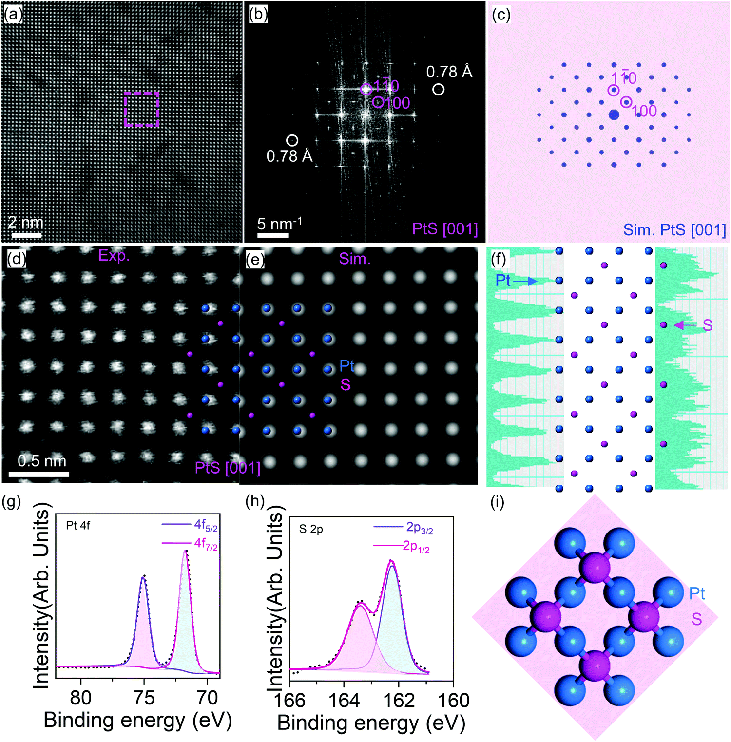 | ||
| Fig. 2 Atomic-resolution imaging of the PtS thin film. (a) STEM graph of PtS. (b) Fast Fourier transform (FFT) pattern derived from the dashed square marked area in panel (a). (c) Simulated electron diffraction pattern of PtS in the [001] direction. (d) The experimental close-up view and (e) the corresponding simulated HAADF-STEM image of PtS along the [001] direction. The superimposed model of PtS is also shown. (f) Atomic model of PtS along the [001] zone axis. XPS spectra of PtS at (g) Pt 4f and (h) S 2p peaks. (i) Primary cell structure of PtS. | ||
The perspective view of the PtS crystal is presented in Fig. 1e. Indeed, the PtS crystal structure has been confirmed with atomic resolution STEM graphs. The PtS film was transferred onto the TEM grid for structural observation (Fig. S2, ESI†). We first look at the simulated electron diffraction patterns (Fig. 1f and h) of PtS at two typical orientations. Then, we observed the sample with the Cs corrected STEM approach and captured the atomic resolution STEM graphs in Fig. 1g and i, which agree well with the PtS [001] and [021], respectively. Here, fake color processing was employed to enhance the contrast of the STEM images.
Now we come to discuss the PtS imaging in detail. Fig. 2 shows the chemically sensitive high-angle annular dark field scanning TEM (HAADF-STEM) characterization of the PtS thin film. A periodic oscillation of intensity is observed from Fig. 2a. The intensity contrast between Pt and S is caused by the Z-contrast of these two elements (Pt, 78 and S, 16).
The corresponding Fast Fourier transform (FFT) pattern indicates that this image was projected along the PtS [001] direction. The diffraction spots of 3.4 and 2.5 Å measured from Fig. 2b match well with lattice spacings of (100) and (1![[1 with combining macron]](https://www.rsc.org/images/entities/char_0031_0304.gif) 0) PtS (ICSD-654379, space group: P42/mmc, a = b = 3.47 Å, c = 6.11 Å, α = β = γ = 90°),26 respectively. The atomic model of PtS along the [001] zone axis and the corresponding simulated HAADF-STEM image match well with the synthetic PtS (Fig. 2d and e).
0) PtS (ICSD-654379, space group: P42/mmc, a = b = 3.47 Å, c = 6.11 Å, α = β = γ = 90°),26 respectively. The atomic model of PtS along the [001] zone axis and the corresponding simulated HAADF-STEM image match well with the synthetic PtS (Fig. 2d and e).
Besides, the intensity profiles (Fig. 2f) were plotted from the vertical lines connecting the bright dots in Fig. 2d. The vertical lines are labelled in Fig. S4 (ESI†). Indeed, the average distance between two adjacent Pt atoms is 0.25 nm (Fig. S4, ESI†), which agrees with the lattice parameter of PtS. Besides, the two neighboring S atoms possess a distance of 0.5 nm (Fig. S5, ESI†), which also matches the PtS lattice. In addition, the Pt–Pt distance along the diagonal direction (Fig. S6, ESI†) is measured as 0.35 nm, which is identical to the S–S distance (Fig. S7, ESI†). This shows a significant difference compared with pure Pt crystals.27
More STEM images showing different orientations, e.g., PtS [021], are shown in Fig. S3 (ESI†). Along the [021] zone axis, the Pt–Pt distance is determined as 0.23 nm (Fig. S8, ESI†). Similarly, the S–S distance remains 0.23 nm (Fig. S9, ESI†), which agrees well with the structural model.26 All these atomic-scale STEM characterization studies clearly evidenced that pure phase PtS formed in the sample.
The grain size was determined by averaging the length and width for each grain by color mapping. This idea was inspired by the relative rotation angle between two adjacent graphene facets with mapping by the dark-field TEM and SAED approach.28–30 Indeed, we have developed this SAED approach to determine the average grain size of 2D materials, as reported in our previous work.31
Besides, the grain size matches well with the aperture size from SAED data. Indeed, under electron-beam irradiation by the aperture size (ca. 220 nm in Fig. S10, ESI†), two sets of diffraction patterns emerge (Fig. S11, ESI†). For a larger aperture size (ca. 860 nm in Fig. S10a, ESI†), twelve sets of diffraction patterns were observed in SAED data (Fig. S12, ESI†). Therefore, the grain size was determined in the range from 220 nm to 290 nm. The number of grains inside the aperture was estimated from SAED patterns (Fig. S10c and d, ESI†). This information confirms the assignment of grains with different image contrasts in STEM micrographs for two neighboring domains (Fig. S13a–c, ESI†). Eventually, the histogram of the average grain size (width) is presented (Fig. S13d, ESI†), ranging from 100 to 500 nm. Therefore, the PtS film was produced with nanocrystalline grains.
X-Ray photoelectron spectroscopy has been employed to obtain the chemical environment of the PtS sample. Indeed, the Pt element (Fig. 2g) shows a doublet peak at 72.1 and 75.5 eV, which corresponds to the featural peaks of Pt 4f 7/2 and Pt 4f 5/2. Besides, the S element (Fig. 2h) demonstrates a doublet peak at 162.6 and 163.6 eV, respectively. These XPS peaks agree well with the reference powder samples of PtS synthesized from the high vacuum annealing of stoichiometrically mixed Pt and S powders.22 The elemental analysis further confirms the successful PtS formation. The PtS primary cell was provided in atomic configuration in the (001) orientation (Fig. 2i).
However, another phase, PtS2, has garnered recent attention due to its excellent electronic properties32–34 and promising applications35 and has been synthesized with the CVD method and observed frequently in recent studies.36
In order to interpret our experimental results and understand the competition between PtS and PtS2 during the CVD growth, we calculated the Gibbs free energy difference (Fig. S14, ESI†) of PtS and PtS2 by tuning the chemical potential of S under certain conditions. Here, G is abbreviated for Gibbs free energy, and ΔG means the change in Gibbs free energy. The transformation of PtS into PtS2 can be interpreted as the addition or incorporation of one S atom into the PtS structure. In this reaction, the change in free energy can be expressed as follows: ΔG = GPtS2− GPtS− NS·μS. The calculation approach is presented in the Experimental section (and more details are presented in the ESI†). In view of thermodynamics, the chemical potential of S species, i.e., the change in the energy of the system upon the incorporation of one S atom, is shown in Fig. 3a at different growth temperatures and sulfur partial pressures. The chemical potential of S (μS) increases as the partial pressure of S vapor increases; however, it decreases when the temperature increases. Indeed, the trends obey the laws of thermodynamics.
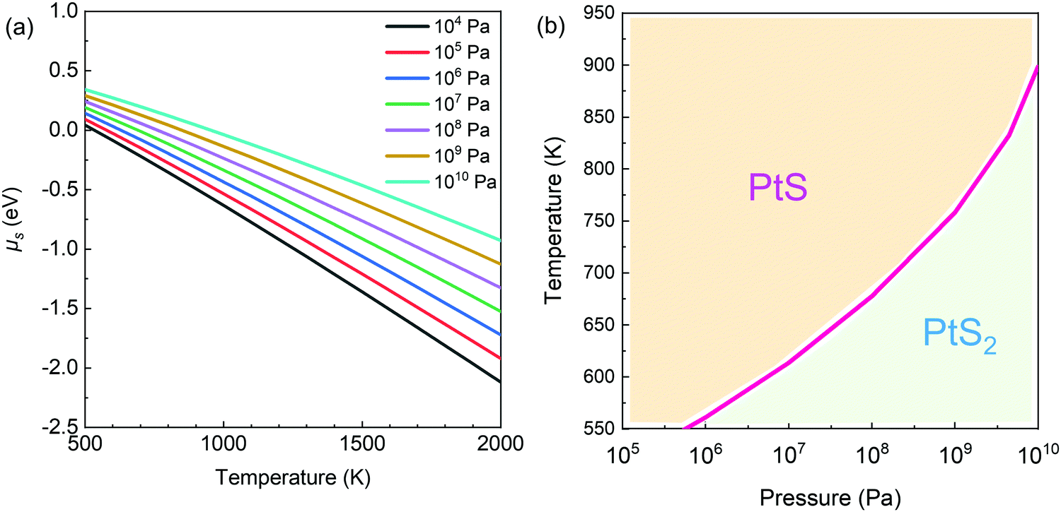 | ||
| Fig. 3 Calculated phase diagram of platinum sulfide. (a) The chemical potential of sulfur in the incorporation into PtS for the formation of PtS2 at different growth temperatures T and partial pressures P of sulfur vapor. (b) Phase diagrams of PtS and PtS2 at different growth temperatures T and sulfur partial pressures P. In thermodynamics, ΔG < 0 occurs in the PtS2 region, while ΔG > 0 is the case in the PtS region. At the boundary, ΔG = 0 for the reaction PtS + S = PtS2. | ||
Then, the phase diagram for the Pt–S compound (Fig. 3b) can be drawn according to the change in Gibbs free energy in the reaction PtS + S = PtS2. Here, PtS seems to be dominating in the top left region (Fig. 3b), i.e., under the condition of high temperature and low sulfur partial pressure, while PtS2 preferably forms in the bottom region (low temperature and high sulfur partial pressure).
Based on the calculated phase diagram (Fig. 3b), PtS tends to form at or below the sulfur partial pressure of 1 atm when the growth temperature is set as 700 °C. During thermal sulfurization, the sulfur partial pressure was much lower than 1 atm (i.e., 0.21 atm). Indeed, the total pressure of the Ar/H2/H2S mixture was maintained at 1 atm. Under the experimental conditions, PtS dominates in the synthetic product after sulfurization of Pt films.
Indeed, our calculation shows validity in interpreting the formation of either PtS or PtS2 under different growth conditions. First, the chemical vapor transport technique leads to formation of bulk crystals of PtS2,35,37–39 in which the confined space of the sealed ampoule facilitates a high partial pressure of S vapor. In contrast, the open-space sintering of mixed Pt/S powders results in the synthesis of PtS crystals40–44 in the early stage or the sulfurization of Pt metal,20,45,46 which provided PtS powders for the XRD investigation to obtain the standard diffraction pattern data. By the tuning of S partial pressure during the annealing, one can convert PtS into PtS2.24,25,47
Our calculation results may provide a general guide for selecting proper parameter windows to synthesize stoichiometric or defective transition metal dichalcogenides, e.g., PtS2, MoS2 or PdS2. For example, one can obtain a stoichiometric MS2-rich film (here M denotes the metal) by the regulation of pressure and temperature, i.e., increasing the partial pressure of sulfur and decreasing the reaction temperature. Similarly, one can selectively grow sub-stoichiometric MSx (1 ≤ x < 2), i.e., containing S vacancies, by regulating the growth parameters of low sulfur pressure and high temperature. In addition, the S-deficient defects can also be induced through the application of external forces, e.g., sonication,48 laser irradiation,49,50 plasma treatment51 or thermal annealing in vacuum.52
After knowing the good material quality of the resultant PtS film, we began to investigate its device performance. PtS films of three different thicknesses were characterized in the first place with optical imaging and Raman spectroscopy (Fig. S15, ESI†). The photodetector was fabricated with direct deposition of the electrode pad (Fig. 4a) over the PtS film on the dielectric substrate, e.g., Si/SiO2.
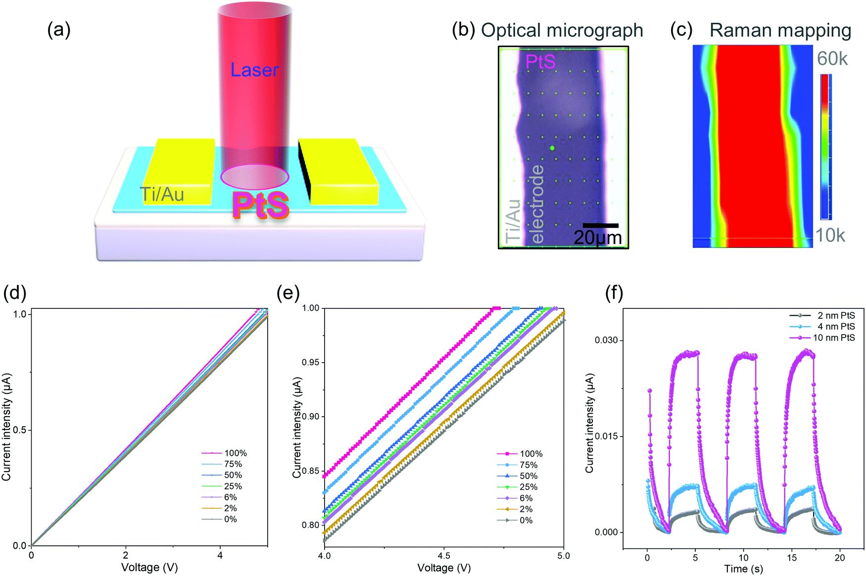 | ||
| Fig. 4 The performance of the PtS based photodetector. (a) Scheme of the device. (b) Optical micrograph of the device. (c) Raman mapping of the B1g mode of PtS. (d) The laser power dependent current. The laser wavelength is 650 nm. (e) Magnified region from panel (d). (f) Time dependent current of the PtS based photodetector with periodical switching on and off of the light source. Different PtS thicknesses of 2 nm, 4 nm and 10 nm were applied for photodetector fabrication. The current intensity was the net photocurrent, i.e., the change in current with turning the light on. | ||
The optical micrograph (Fig. 4b) and Raman mapping of the B1g mode (Fig. 4c) confirmed the successful device fabrication. The PtS based photodetector has shown an excellent photocurrent response upon light irradiation of increasing laser power (Fig. 4d). Indeed, the magnified line curves (Fig. 4e) clearly demonstrated the increase of photocurrent intensity upon the increase of laser power.
Besides, it shows a significant photocurrent response with the illumination of 2% laser power (ca. 4 mW). Eventually, we investigated the effect of PtS thickness on the device performance, i.e., photocurrent curves upon the illumination (Fig. 4f). Dark currents of 0.50, 0.70, and 1.01 μA were provided corresponding to the PtS based devices with film thicknesses of 2, 4, and 10 nm, respectively, for comparison. The 10 nm PtS based photodetector shows superior photocurrent compared with the 2 nm and 4 nm counterparts. The thickness of PtS films was determined by AFM height profiles (Fig. S16, ESI†). Here, the surface roughness is presented (Table S1, ESI†). Therefore, the optimal PtS thickness for the photodetector was determined as 10 nm in this study.
We have evaluated the device performances with the approach of determining the rise time and decay time of the photodetectors.53–56 The rise time and decay time were extracted as 0.29 s and 0.82 s from Fig. S17 (ESI†), respectively. With the regulation of laser power, one can collect the power-dependent photocurrent curves and obtain the responsivity57–60 and detectivity61–64 of a photodetector. We have obtained a responsivity of 201 mA W−1 and a detectivity of 5.3 × 10⁹ Jones from Fig. S17a (ESI†). The PtS film shows good absorbance in the UV-vis and near-infrared range (Fig. S18, ESI†). Indeed, the PtS based photodetector exhibited analogous photocurrent performances under illumination of three typical wavelengths (Fig. S19, ESI†). Therefore, the PtS film shows excellent potential for a full spectral photoelectronic response, which is highly desired in image sensors.
Our PtS based device showed a comparable performance, with some parameters exceeding those of devices based on Pt chalcogenides (Table 1). Moreover, the 2D PtS thin film can be synthesized over a wafer scale, which has great potential for large-area image sensors based on arrayed photodetectors.
Our facile metal-sulfurization strategy has led to the synthesis of a 4-inch wafer-scale homogeneous PtS film. Besides, the atomic resolution STEM imaging and diffraction simulation confirm the formation of pure phase PtS. Furthermore, the thermodynamically calculated phase diagram of the Pt–S compound has shown dominant PtS formation other than PtS2 under our experimental conditions. Eventually, the PtS-based photodetector has demonstrated a superior photoresponse and large photocurrent generation. Our approach may shed light on the large area integration of PtS into 2D material-based van der Waals heterostructures67–71 as well as their electronic and photoelectronic applications.
Experimental section
Materials synthesis
PtS thin films were synthesized through metal film plus post-sulfurization treatment. The Pt films were deposited on the substrate using an electron beam evaporation furnace (model: HHV ATS500). The film thickness was controlled by a controller with a crystal oscillator. Different substrates were employed to host Pt film deposition such as quartz and Si/SiO2 wafers. The Pt films were mounted in the horizontal tube furnace. Then the furnace was evacuated to remove oxygen, flushed with Ar gas and then filled with an Ar/H2 mixture (225 sccm/75 sccm). After heating the substrate to a typical temperature, i.e., 700 °C, a flow of 80 sccm H2S was introduced for sulfurization. The partial pressure of sulfur was estimated as 21% (80 sccm H2S in 380 sccm total gases). The temperature has been regulated from 600, 650, 700, 750, and 800 °C. Different sulfurization durations ranging from 30 min to 3 h were applied. Eventually, the samples were cooled with an air ventilator by moving the horizontal tube furnace (on a sliding rail) out of the zone of substrates. When the temperature drops to 25 °C, the samples were taken out for characterization and device fabrication.Materials characterization tools
The following instruments were employed, i.e., a Raman spectrometer (Horiba LabRAM HR Evolution with an excitation wavelength of 532 nm), an optical microscope (Olympus BX53MRF-S), an atomic force microscope (Bruker Dimension Icon) and an X-ray photoelectron spectrometer (model: AXIS Supra) for chemical environment analysis.TEM characterization of the PtS film
The PtS film was transferred from the Si/SiO2 substrate onto the TEM grid with a polymer-assisted transfer approach.31,72–75 STEM experiments were performed on a Double Cs-corrected FEI Titan Cube transmission electron microscope (300 kV). The simulated STEM images of PtS [001] were obtained using a quantitative STEM simulation package (see the ESI† for more details).DFT computations
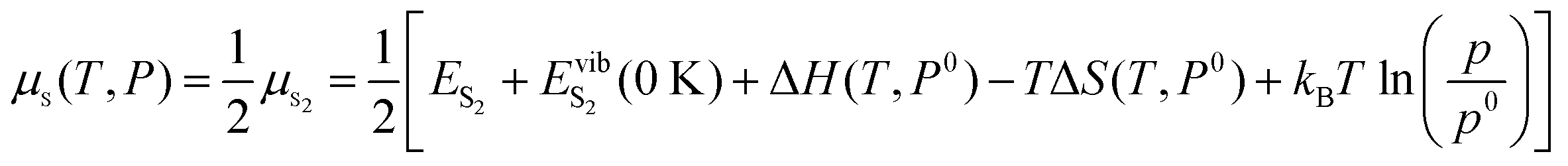
Density functional theory was employed for the computations of the chemical potential of sulfur and the Gibbs free energies of PtS and PtS2. More details on the simulation package,76,77 approximation78 and algorithm79,80 are provided in the ESI† (including other calculation parameters).81The thermodynamic phase diagram was explored by comparing the difference of the Gibbs free energy ΔG between PtS and PtS2 as follows:
| ΔG = GPtS2 − GPtS − NSμS | (1) |
| G(P,T) = Fphonon + PV | (2) |
 | (3) |
 | (4) |
Here ES2 is the calculated energy of an isolated S dimer (denoted as S2) molecule and EvibS2 (0 K) corresponds to the zero-point vibrational energy, also obtained from the calculations, p is the partial pressure of sulfur and p0 is the standard pressure which is 105 Pa. Changes in both the enthalpy and entropy of S dimer S2 are extracted from the thermochemical tables83 at p0 = 105 Pa.
Device fabrication and performance examination
The photodetector devices were directly fabricated on Si/SiO2 substrates by depositing electrode pads over PtS films. Electron beam evaporation (with HHV ATS 500 evaporator equipment) was employed to deposit 10 nm Ti and 50 nm Au patterns over PtS films through a hard stainless-steel mask. The channel length between two electrodes was 50 μm. The measurements of photocurrent responses were made using a Keithley 2400. The laser light source for illumination has a wavelength of 650 nm and a full power of 200 mW. Neutral density filters were used for regulating the laser power during light irradiation.Author contributions
Jinbo Pang: conceptualization, methodology, investigation, writing – original draft preparation; Yanhao Wang & Yu Zhang: data curation – electronic device data collection; Lei Zhang & Feng Yang: data curation – TEM and SAED data collection; Xiaoxin Yang & Xiao Wang: software, data curation – phase diagram calculation; Yufen Li: investigation; Jiali Yang: visualization, validation; Gianaurelio Cuniberti: software, project administration; Hong Liu: supervision, writing – editing, funding acquisition; Mark H Rümmeli: validation, writing – review and editing.Conflicts of interest
There are no conflicts of interest to declare.Acknowledgements
The authors show their gratitude to the National Natural Science Foundation of China (NSFC, grant no. 51802116), the Natural Science Foundation of Shandong Province (grant no. ZR2019BEM040), the State Key Laboratory of Biobased Material and Green Papermaking (Qilu University of Technology, Shandong Academy of Sciences, grant no. GZKF202107), the National Key Research and Development Program of China (2017YFB0405400) from the Ministry of Science and Technology (MOST) of China, the Natural Science Foundation for Distinguished Young Scientists of Shandong Province (grant no. JQ201814), the Project of “20 items of University” of Jinan (2018GXRC031), Taishan Scholars Project Special Funds (tsqn201812083) and the NSFC (No. 52022037). X. W. acknowledges funding by the NSFC (22003074), the State Key Laboratory of Mechanics and Control of Mechanical Structures (Nanjing University of Aeronautics and Astronautics) (MCMS-E-0420G01) and the SIAT Innovation Program for Excellent Young Researchers. F. Y. was supported by the National Key Research and Development Program of China (2021YFA0717400), the National Natural Science Foundation of China (92161124 and 52002165), Beijing National Laboratory for Molecular Sciences (BNLMS202013), Shenzhen Basic Research Project (JCYJ20170817113121505 and JCYJ20210324104808022), Guangdong Provincial Natural Science Foundation (2021A1515010229), Guangdong Provincial Innovation Project (2019KTSCX155), and Guangdong Provincial Key Laboratory of Catalysis (2020B121201002). M. H. R. thanks the National Science Foundation China (NSFC, Project 52071225), the National Science Center and the Czech Republic under the ERDF program “Institute of Environmental Technology—Excellent Research” (No. CZ.02.1.01/0.0/0.0/16_019/0000853) and the Sino-German Research Institute for support (Project No. GZ 1400).References
- K. S. Novoselov, A. Mishchenko, A. Carvalho and A. H. Castro Neto, Science, 2016, 353, aac9439 CrossRef CAS PubMed.
- Y. Liu, N. O. Weiss, X. Duan, H.-C. Cheng, Y. Huang and X. Duan, Nat. Rev. Mater., 2016, 1, 16042 CrossRef CAS.
- D. Jariwala, T. J. Marks and M. C. Hersam, Nat. Mater., 2017, 16, 170–181 CrossRef CAS PubMed.
- Z. Zheng, J. Yao, J. Li and G. Yang, Mater. Horiz., 2020, 7, 2185–2207 RSC.
- F. Wang, Z. Wang, T. A. Shifa, Y. Wen, F. Wang, X. Zhan, Q. Wang, K. Xu, Y. Huang, L. Yin, C. Jiang and J. He, Adv. Funct. Mater., 2017, 27, 1603254 CrossRef.
- F. Wang, Z. Wang, L. Yin, R. Cheng, J. Wang, Y. Wen, T. A. Shifa, F. Wang, Y. Zhang, X. Zhan and J. He, Chem. Soc. Rev., 2018, 47, 6296–6341 RSC.
- D. Wu, Z. Zhao, W. Lu, L. Rogée, L. Zeng, P. Lin, Z. Shi, Y. Tian, X. Li and Y. H. Tsang, Nano Res., 2021, 14, 1973–1979 CrossRef CAS.
- D. Wu, J. Guo, C. Wang, X. Ren, Y. Chen, P. Lin, L. Zeng, Z. Shi, X. J. Li, C. X. Shan and J. Jie, ACS Nano, 2021, 15, 10119–10129 CrossRef PubMed.
- D. Wu, J. Guo, J. Du, C. Xia, L. Zeng, Y. Tian, Z. Shi, Y. Tian, X. J. Li, Y. H. Tsang and J. Jie, ACS Nano, 2019, 13, 9907–9917 CrossRef CAS PubMed.
- D. Wu, Z. Mo, Y. Han, P. Lin, Z. Shi, X. Chen, Y. Tian, X. J. Li, H. Yuan and Y. H. Tsang, ACS Appl. Mater. Interfaces, 2021, 13, 41791–41801 CrossRef CAS PubMed.
- D. Wu, C. Jia, F. Shi, L. Zeng, P. Lin, L. Dong, Z. Shi, Y. Tian, X. Li and J. Jie, J. Mater. Chem. A, 2020, 8, 3632–3642 RSC.
- D. Wu, C. Guo, Z. Wang, X. Ren, Y. Tian, Z. Shi, P. Lin, Y. Tian, Y. Chen and X. Li, Nanoscale, 2021, 13, 13550–13557 RSC.
- A. Marmier, P. S. Ntoahae, P. E. Ngoepe, D. G. Pettifor and S. C. Parker, Phys. Rev. B: Condens. Matter Mater. Phys., 2010, 81, 172102 CrossRef.
- V. I. Rozhdestvina, A. A. Udovenko, S. V. Rubanov and N. V. Mudrovskaya, Crystallogr. Rep., 2016, 61, 193–202 CrossRef CAS.
- A. Kjekshus, Acta Chem. Scand., 1961, 15, 159–166 CrossRef CAS.
- R. Collins, R. Kaner, P. Russo, A. Wold and D. Avignant, Inorg. Chem., 2002, 18, 727–729 CrossRef.
- P. Raybaud, J. Hafner, G. Kresse and H. Toulhoat, J. Phys.: Condens. Matter, 1997, 9, 11107–11140 CrossRef CAS.
- J. C. Harms, L. C. O'Brien and J. J. O'Brien, J. Chem. Phys., 2019, 151, 094303 CrossRef PubMed.
- C. P. Cullen, C. O. Coileáin, J. B. McManus, O. Hartwig, D. McCloskey, G. S. Duesberg and N. McEvoy, Nanoscale, 2021, 13, 7403–7411 RSC.
- J. Huang, N. Dong, N. McEvoy, L. Wang, C. O. Coileain, H. Wang, C. P. Cullen, C. Chen, S. Zhang, L. Zhang and J. Wang, ACS Nano, 2019, 13, 13390–13402 CrossRef CAS PubMed.
- M. S. Shawkat, S. S. Han, H. S. Chung, S. A. Mofid, C. Yoo and Y. Jung, Adv. Electron. Mater., 2021, 7, 2100395 CrossRef CAS.
- J. Dembowski, L. Marosi and M. Essig, Surf. Sci. Spectra, 1993, 2, 104–108 CrossRef CAS.
- N. Ramasubramanian, J. Electroanal. Chem. Interfacial Electrochem., 1975, 64, 21–37 CrossRef CAS.
- R. Kempt, A. Kuc and T. Heine, Angew. Chem., Int. Ed., 2020, 59, 9242–9254 CrossRef CAS PubMed.
- D. Zhao, S. Xie, Y. Wang, H. Zhu, L. Chen, Q. Sun and D. W. Zhang, AIP Adv., 2019, 9, 025225 CrossRef.
- K. Persson, Materials Data on PtS (SG:131) by Materials Project, 2014, vol. 1 DOI:10.17188/1202853.
- K. Persson, Materials Data on Pt (SG:225) by Materials Project, 2015, vol. 1 DOI:10.17188/1189002.
- P. Y. Huang, C. S. Ruiz-Vargas, A. M. van der Zande, W. S. Whitney, M. P. Levendorf, J. W. Kevek, S. Garg, J. S. Alden, C. J. Hustedt, Y. Zhu, J. Park, P. L. McEuen and D. A. Muller, Nature, 2011, 469, 389–392 CrossRef CAS PubMed.
- A. M. van der Zande, P. Y. Huang, D. A. Chenet, T. C. Berkelbach, Y. You, G. H. Lee, T. F. Heinz, D. R. Reichman, D. A. Muller and J. C. Hone, Nat. Mater., 2013, 12, 554–561 CrossRef CAS PubMed.
- M. P. Levendorf, C. J. Kim, L. Brown, P. Y. Huang, R. W. Havener, D. A. Muller and J. Park, Nature, 2012, 488, 627–632 CrossRef CAS PubMed.
- J. Pang, R. G. Mendes, P. S. Wrobel, M. D. Wlodarski, H. Q. Ta, L. Zhao, L. Giebeler, B. Trzebicka, T. Gemming, L. Fu, Z. Liu, J. Eckert, A. Bachmatiuk and M. H. Rummeli, ACS Nano, 2017, 11, 1946–1956 CrossRef CAS PubMed.
- R. A. B. Villaos, C. P. Crisostomo, Z.-Q. Huang, S.-M. Huang, A. A. B. Padama, M. A. Albao, H. Lin and F.-C. Chuang, npj 2D Mater. Appl., 2019, 3, 2 CrossRef.
- M. Sajjad, N. Singh and U. Schwingenschlögl, Appl. Phys. Lett., 2018, 112, 043101 CrossRef.
- Y. Zhao, J. Qiao, P. Yu, Z. Hu, Z. Lin, S. P. Lau, Z. Liu, W. Ji and Y. Chai, Adv. Mater., 2016, 28, 2399–2407 CrossRef CAS PubMed.
- Z. Wang, P. Wang, F. Wang, J. Ye, T. He, F. Wu, M. Peng, P. Wu, Y. Chen, F. Zhong, R. Xie, Z. Cui, L. Shen, Q. Zhang, L. Gu, M. Luo, Y. Wang, H. Chen, P. Zhou, A. Pan, X. Zhou, L. Zhang and W. Hu, Adv. Funct. Mater., 2019, 30, 1907945 CrossRef.
- H. Xu, H. P. Huang, H. Fei, J. Feng, H. R. Fuh, J. Cho, M. Choi, Y. Chen, L. Zhang, D. Chen, D. Zhang, C. O. Coileain, X. Han, C. R. Chang and H. C. Wu, ACS Appl. Mater. Interfaces, 2019, 11, 8202–8209 CrossRef CAS PubMed.
- Y. Sato, T. Nishimura, D. Duanfei, K. Ueno, K. Shinokita, K. Matsuda and K. Nagashio, Adv. Electron. Mater., 2021, 7, 2100292 CrossRef CAS.
- X. Wang, H. Long, W. Qarony, C. Y. Tang, H. Yuan and Y. H. Tsang, J. Lumin., 2019, 211, 227–232 CrossRef.
- A. Finley, D. Schleich, J. Ackerman, S. Soled and A. Wold, Mater. Res. Bull., 1974, 9, 1655–1659 CrossRef CAS.
- M. A. Malik, P. O’Brien and N. Revaprasadu, J. Mater. Chem., 2002, 12, 92–97 RSC.
- B. Z. Li, K. Y. Jung and T. C. Steimle, J. Mol. Spectrosc., 1995, 170, 310–322 CrossRef CAS.
- F. Grønvold, T. Thurmann-Moe, E. F. Westrum and E. Chang, J. Chem. Phys., 1961, 35, 1665–1669 CrossRef.
- F. Grønvold, H. Haraldsen, A. Kjekshus and R. Söderquist, Acta Chem. Scand., 1960, 14, 1879–1893 CrossRef.
- J. E. Mungall, D. R. A. Andrews, L. J. Cabri, P. J. Sylvester and M. Tubrett, Geochim. Cosmochim. Acta, 2005, 69, 4349–4360 CrossRef CAS.
- S. Monaghan, E. M. Coleman, L. Ansari, J. Lin, A. Buttimer, P. A. Coleman, J. Connolly, I. M. Povey, B. Kelleher, C. Ó. Coileáin, N. McEvoy, P. K. Hurley and F. Gity, Appl. Mater. Today, 2021, 25, 101163 CrossRef.
- B. Lin, Y. Zhou, B. Xu, C. Zhu, W. Tang, Y. Niu, J. Di, P. Song, J. Zhou, X. Luo, L. Kang, R. Duan, Q. Fu, H. Liu, R. Jin, C. Xue, Q. Chen, G. Yang, K. Varga, Q. Xu, Y. Li, Z. Liu and F. Liu, Mater. Horiz., 2021, 8, 612–618 RSC.
- J. Lu, X. Zhang, G. Su, W. Yang, K. Han, X. Yu, Y. Wan, X. Wang and P. Yang, Mater. Today Phys., 2021, 18, 100376 CrossRef CAS.
- J. Liu, H. Xu, J. Yan, J. Huang, Y. Song, J. Deng, J. Wu, C. Ding, X. Wu, S. Yuan and H. Li, J. Mater. Chem. A, 2019, 7, 18906–18914 RSC.
- Q. Liang, Q. Zhang, X. Zhao, M. Liu and A. T. S. Wee, ACS Nano, 2021, 15, 2165–2181 CrossRef CAS PubMed.
- X. Yin, C. S. Tang, Y. Zheng, J. Gao, J. Wu, H. Zhang, M. Chhowalla, W. Chen and A. T. S. Wee, Chem. Soc. Rev., 2021, 50, 10087–10115 RSC.
- Q. Liang, Q. Zhang, J. Gou, T. Song, Arramel, H. Chen, M. Yang, S. X. Lim, Q. Wang, R. Zhu, N. Yakovlev, S. C. Tan, W. Zhang, K. S. Novoselov and A. T. S. Wee, ACS Nano, 2020, 14, 5668–5677 CrossRef CAS PubMed.
- R. Chua, J. Yang, X. He, X. Yu, W. Yu, F. Bussolotti, P. K. J. Wong, K. P. Loh, M. B. H. Breese, K. E. J. Goh, Y. L. Huang and A. T. S. Wee, Adv. Mater., 2020, 32, 2000693 CrossRef CAS PubMed.
- Z. Zheng, L. Gan, J. Zhang, F. Zhuge and T. Zhai, Adv. Sci., 2017, 4, 1600316 CrossRef PubMed.
- R. Zhuo, L. Zeng, H. Yuan, D. Wu, Y. Wang, Z. Shi, T. Xu, Y. Tian, X. Li and Y. H. Tsang, Nano Res., 2018, 12, 183–189 CrossRef.
- L. Zeng, S. Lin, Z. Lou, H. Yuan, H. Long, Y. Li, W. Lu, S. P. Lau, D. Wu and Y. H. Tsang, NPG Asia Materials, 2018, 10, 352–362 CrossRef CAS.
- Q. Zhao, W. Wang, F. Carrascoso-Plana, W. Jie, T. Wang, A. Castellanos-Gomez and R. Frisenda, Mater. Horiz., 2020, 7, 252–262 RSC.
- H. Wang, Z. Li, D. Li, P. Chen, L. Pi, X. Zhou and T. Zhai, Adv. Funct. Mater., 2021, 31, 2103106 CrossRef CAS.
- S. Yang, P. Luo, F. Wang, T. Liu, Y. Zhao, Y. Ma, H. Li and T. Zhai, Small, 2021, 2105211, DOI:10.1002/smll.202105211.
- M. Dai, H. Chen, F. Wang, M. Long, H. Shang, Y. Hu, W. Li, C. Ge, J. Zhang, T. Zhai, Y. Fu and P. Hu, ACS Nano, 2020, 14, 9098–9106 CrossRef CAS PubMed.
- D. Wu, Y. Wang, L. Zeng, C. Jia, E. Wu, T. Xu, Z. Shi, Y. Tian, X. Li and Y. H. Tsang, ACS Photonics, 2018, 5, 3820–3827 CrossRef CAS.
- M. Zhao, J. Su, Y. Zhao, P. Luo, F. Wang, W. Han, Y. Li, X. Zu, L. Qiao and T. Zhai, Adv. Funct. Mater., 2020, 30, 1909849 CrossRef CAS.
- W. Han, C. Li, S. Yang, P. Luo, F. Wang, X. Feng, K. Liu, K. Pei, Y. Li, H. Li, L. Li, Y. Gao and T. Zhai, Small, 2020, 16, 2000228 CrossRef CAS PubMed.
- Z. Wang, P. Luo, B. Han, X. Zhang, S. Zhao, S. Wang, X. Chen, L. Wei, S. Yang, X. Zhou, S. Wang, X. Tao and T. Zhai, ACS Nano, 2021, 15(12), 20442–20452 CrossRef CAS PubMed.
- C. Chang, W. Chen, Y. Chen, Y. Chen, Y. Chen, F. Ding, C. Fan, H. Jin Fan, Z. Fan, C. Gong, Y. Gong, Q. He, X. Hong, S. Hu, W. Hu, W. Huang, Y. Huang, W. Ji, D. Li, L.-J. Li, Q. Li, L. Lin, C. Ling, M. Liu, N. Liu, Z. Liu, K. Ping Loh, J. Ma, F. Miao, H. Peng, M. Shao, L. Song, S. Su, S. Sun, C. Tan, Z. Tang, D. Wang, H. Wang, J. Wang, X. Wang, X. Wang, A. T. S. Wee, Z. Wei, Y. Wu, Z.-S. Wu, J. Xiong, Q. Xiong, W. Xu, P. Yin, H. Zeng, Z. Zeng, T. Zhai, H. Zhang, H. Zhang, Q. Zhang, T. Zhang, X. Zhang, L.-D. Zhao, M. Zhao, W. Zhao, Y. Zhao, K.-G. Zhou, X. Zhou, Y. Zhou, H. Zhu, H. Zhang and Z. Liu, Acta Phys. – Chim. Sin., 2021, 37, 2108017 Search PubMed.
- Z. X. Zhang, Z. Long-Hui, X. W. Tong, Y. Gao, C. Xie, Y. H. Tsang, L. B. Luo and Y. C. Wu, J. Phys. Chem. Lett., 2018, 9, 1185–1194 CrossRef CAS PubMed.
- J. Yuan, T. Sun, Z. Hu, W. Yu, W. Ma, K. Zhang, B. Sun, S. P. Lau, Q. Bao, S. Lin and S. Li, ACS Appl. Mater. Interfaces, 2018, 10, 40614–40622 CrossRef CAS PubMed.
- J. Jiang, F. Meng, Q. Cheng, A. Wang, Y. Chen, J. Qiao, J. Pang, W. Xu, H. Ji, Y. Zhang, Q. Zhang, S. Wang, X. Feng, L. Gu, H. Liu and L. Han, Small Methods, 2020, 4, 2070032 CrossRef CAS.
- J. F. Jiang, F. Q. Meng, Q. L. Cheng, A. Z. Wang, Y. K. Chen, J. Qiao, J. B. Pang, W. D. Xu, H. Ji, Y. Zhang, Q. H. Zhang, S. P. Wang, X. J. Feng, L. Gu, H. Liu and L. Han, Small Methods, 2020, 4, 2000238 CrossRef CAS.
- Y. Wang, J. Pang, Q. Cheng, L. Han, Y. Li, X. Meng, B. Ibarlucea, H. Zhao, F. Yang, H. Liu, H. Liu, W. Zhou, X. Wang, M. H. Rummeli, Y. Zhang and G. Cuniberti, Nano-Micro Lett., 2021, 13, 143 CrossRef CAS PubMed.
- Q. Cheng, J. Pang, D. Sun, J. Wang, S. Zhang, F. Liu, Y. Chen, R. Yang, N. Liang, X. Lu, Y. Ji, J. Wang, C. Zhang, Y. Sang, H. Liu and W. Zhou, InfoMat, 2020, 2, 656–697 CrossRef CAS.
- B. J. Sun, J. Pang, Q. L. Cheng, S. Zhang, Y. F. Li, C. C. Zhang, D. H. Sun, B. Ibarlucea, Y. Li, D. Chen, H. M. Fan, Q. F. Han, M. X. Chao, H. Liu, J. G. Wang, G. Cuniberti, L. Han and W. J. Zhou, Adv. Mater. Technol., 2021, 6, 2000744 CrossRef.
- L. Ding, A. Tselev, J. Wang, D. Yuan, H. Chu, T. P. McNicholas, Y. Li and J. Liu, Nano Lett., 2009, 9, 800–805 CrossRef CAS PubMed.
- Q. Hao, J. Pang, Y. Zhang, J. W. Wang, L. B. Ma and O. G. Schmidt, Adv. Opt. Mater., 2018, 6, 1700984 CrossRef.
- R. G. Mendes, J. Pang, A. Bachmatiuk, H. Q. Ta, L. Zhao, T. Gemming, L. Fu, Z. Liu and M. H. Rummeli, ACS Nano, 2019, 13, 978–995 CAS.
- Y. Yin, J. Pang, J. Wang, X. Lu, Q. Hao, E. Saei Ghareh Naz, X. Zhou, L. Ma and O. G. Schmidt, ACS Appl. Mater. Interfaces, 2019, 11, 15891–15897 CrossRef CAS PubMed.
- G. Kresse and J. Furthmuller, Phys. Rev. B: Condens. Matter Mater. Phys., 1996, 54, 11169–11186 CrossRef CAS PubMed.
- G. Kresse and J. Furthmüller, Comput. Mater. Sci., 1996, 6, 15–50 CrossRef CAS.
- J. P. Perdew, K. Burke and M. Ernzerhof, Phys. Rev. Lett., 1996, 77, 3865–3868 CrossRef CAS PubMed.
- G. Kresse and D. Joubert, Phys. Rev. B: Condens. Matter Mater. Phys., 1999, 59, 1758–1775 CrossRef CAS.
- P. E. Blöchl, Phys. Rev. B: Condens. Matter Mater. Phys., 1994, 50, 17953–17979 CrossRef PubMed.
- H. J. Monkhorst and J. D. Pack, Phys. Rev. B: Solid State, 1976, 13, 5188–5192 CrossRef.
- M. V. Bollinger, K. W. Jacobsen and J. K. Nørskov, Phys. Rev. B: Condens. Matter Mater. Phys., 2003, 67, 5410 Search PubMed.
- P. J. Linstrom and W. G. Mallard, NIST Chem, WebBook, 2018, vol. 1 DOI:10.18434/T18434D18303.
Footnotes |
| † Electronic supplementary information (ESI) available. See DOI: 10.1039/d1ma00757b |
| ‡ These authors contributed equally to this work. |
| This journal is © The Royal Society of Chemistry 2022 |