
 Open Access Article
 This Open Access Article is licensed under a Creative Commons Attribution-Non Commercial 3.0 Unported Licence
Controlling the interfacial reactions and environment of rare-earth ions in thin oxide films towards wafer-scalable quantum technologies†
N.
Harada
a,
A.
Tallaire
a,
D.
Serrano
a,
A.
Seyeux
a,
P.
Marcus
a,
X.
Portier
b,
C.
Labbé
b,
P.
Goldner
 a and
A.
Ferrier
*ac
a and
A.
Ferrier
*ac
aChimie Paris Tech, PSL University, CNRS, Institut de Recherche de Chimie Pairs, Paris, 75005, France. E-mail: alban.ferrier@chimieparistech.psl.eu
bCIMAP, CEA, UMR CNRS 6252, ENSICAEN, Normandie Université, Caen Cedex 04 14050, France
cFaculté des Sciences et Ingénierie, Sorbonne Universités, UFR 933, Paris 7505, France
First published on 18th October 2021
Abstract
Rare earth (RE) doped oxides have demonstrated great potential for photonic applications and have also appeared as promising candidates for quantum memory devices and microwave to optical transducers. Here, we investigate the potential of Chemical Vapor Deposited (CVD) europium-doped Y2O3 thin films on silicon as a new platform for integrated quantum devices. We aim at improving the optical properties of such thin films by carefully controlling the RE ion's environment. In particular, we study the effect of annealing post treatments and demonstrate that a significant source of broadening of the optical transition arises from interfacial reactions with the silicon substrate. We thus propose to encapsulate RE ions between undoped high-quality thick layers in order to limit the impact of interfacial reactions on their properties during thermal annealing. Using this approach, we succeeded in measuring a narrow inhomogeneous linewidth of 18 GHz and an ultra-narrow homogeneous linewidth of 5 MHz inferred from spectral hole width. These results are promising towards the use of these engineered RE doped thin films for the development of a scalable nanostructured spin-photon interface. In addition, our strategy could be applied to a large variety of oxide films for a broad range of applications.
Introduction
Rare earth doped oxides (REOs) constitute a promising material system for quantum technologies.1,2 Their uniqueness stems from their electronic configuration in which the optical transitions of interest occur between 4f electrons that are shielded by closed shells, setting them akin to atoms naturally trapped inside a crystalline matrix. They offer exceptionally long optical coherence lifetimes, up to 4.4 ms,3 and record spin coherence lifetimes of 6 h4 at cryogenic temperatures. RE elements are also easily exchangeable and provide a wide range of optical transitions including the technologically useful telecom wavelength (with Er3+ at 1530 nm) suitable for fiber-based quantum communications5 and coherent microwave to optical transduction.6 In addition, the possibility of individually addressing single ions within an inhomogeneously broadened linewidth has recently been highlighted as a great advantage for the development of scalable qubit architectures for quantum computing.7Bulk single crystals, such as RE doped Y2SiO5 (YSO), grown by pulling techniques have been largely used for those demonstrations as they provide a well-controlled and high crystalline quality environment for the ions.3,8–10 Nevertheless, their integration into practical and scalable quantum devices, resonators or hybrid structures is limited by the bulky nature of those systems. In fact, processing them by a top-down approach into nanoscale systems in which single ion emitters are precisely spatially localized and addressable represents an important challenge in those macro-systems.11–13 As an alternative, specially designed and optimized Eu:Y2O3 nanoparticles have been recently developed leading to record optical and spin coherence times14–17 for a nanoscale material and have opened up interesting integration perspectives to cavities.18
Beyond the development of those systems, a compact, wafer-scalable thin film platform would be a great asset19 to develop new functionalities including the coupling of a RE doped film with cavities,20 graphene layers21 or into a waveguide structure.22 In addition, such thin films could be compatible with silicon photonic technologies23,24 and they favor an efficient control and spatial localization of dopants within the crystalline matrix25,26 with applications in quantum sensing27 or single ion spectroscopy for quantum computing.28,29 Currently, the main challenge in nanometer thin films is to preserve the extremely narrow optical and spin homogeneous linewidth related to the long coherence properties of RE ions against the presence of surface defects and impurities. Recently we have assessed the potential of both Atomic Layer Deposited (ALD)30 and Chemical Vapor Deposited (CVD)31 Eu-doped Y2O3 films and managed to successfully burn spectral holes with a 22 MHz linewidth in the CVD films. This is at the state-of-the-art for thin films but still an order of magnitude larger than in optimized nanoparticles.17,32 This suggests that additional dephasing mechanisms intrinsic to thin films exist due to interactions with various defects, grain boundaries, residual disorder or strain.33
One way to reduce native defects in as-grown films is to use a high-temperature annealing post treatment.17 The temperature and duration of this post treatment are key parameters since thermally activated diffusion of impurities or reactions with the substrate are known to take place. For example, although post-growth thermal annealing of ALD Eu:Y2O3 films on silicon substrates allowed obtaining narrow and well-resolved emission lines, annealing temperatures (TA) are limited to less than 950 °C before reaction with the silicon substrate leading to parasitic silicate phases.23,26,34
In this work we aim at reducing the optical transition linewidth of Eu-doped Y2O3 thin films grown by CVD on silicon substrates. A comprehensive study by transmission electron microscopy (TEM), time of flight secondary ion mass spectrometry (TOF SIMS), photoluminescence (PL) and high-resolution optical spectroscopy allowed us to reveal Si4+ diffusion in the oxide layer and interfacial oxidation of the substrate during the different post-treatments (conventional or rapid thermal annealing). We probe their impact on the inhomogeneous (ΓIn) and homogeneous linewidths (Γhom) of Eu optical transitions by high resolution and spectral hole burning (SHB) spectroscopies. Encapsulating the active layer containing the RE ions of interest in between high-quality thick undoped oxide layers is proposed as an efficient way to control interfacial reactions and limit their effect on the RE optical properties. Based on these strategies we report ultra-narrow inhomogeneous (18 GHz) and homogeneous (5 MHz) linewidths for Eu:Y2O3 films.
Experimental
Thin film growth
All the thin films produced for this study were grown in a homemade Direct Liquid Injection Chemical Vapor Deposition (DLI-CVD) reactor. The RE precursors used are beta-diketonate complexes: Y(tmhd)3 and Eu(tmhd)3 with a 3N purity were purchased from Strem Chemicals. Once dissolved in mesitylene (99% purity from Alfa Aesar) with concentrations of 0.01 mol L−1 for the yttrium precursor and of 0.001 mol L−1 for europium, the liquid goes through injectors where the aerosol produced is flashily vaporized at 200 °C. The precursors’ vapors are then carried to the reaction chamber by N2 and mixed with O2 so that the deposition of the oxide occurs at a pressure of about 10 mbar. The thin film grows by the heterogeneous reaction between the gaseous phases of RE precursors on 2-inch (111) oriented silicon substrates heated to 650 °C as measured using an optical pyrometer. The amount of precursors, yttrium for the host and europium for the doping, brought into the chamber is precisely controlled by the injection frequency and opening time of the two Kemstream injectors. In situ Spectroscopic Ellipsometry (SE) with a Woollam iSE system is used during deposition to monitor the oxide growth rate (around 300 nm h−1). More details about the growth process are presented in the ESI,† Fig. S1, and in a previous work.35 Multi-layered (doped or undoped) films, with thicknesses varying from a few tens of nm up to 2 μm, were produced in this study.Prior to the deposition, the (111) silicon wafers were wet cleaned using the standard RCA (Radio Corporation of America) protocol.36,37 This chemical treatment removes the native oxide from the surface and leads to a clean surface. The substrate is then placed inside an AS-ONE Rapid Thermal Annealing (RTA) furnace from Annealsys, where a 15 °C s−1 ramp is applied followed by a 10 s step at 1100 °C under an oxygen atmosphere in order to build a 10 nm dense and stable thermal silicon oxide.
TOF-SIMS
The films’ chemical composition was analyzed using a dual-beam TOF-SIMS V spectrometer (ION-TOF GmbH, Muenster, Germany). We measured the depth profile of different ions at a sufficiently low primary ion dose density to keep static conditions. Charge compensation was performed using an electron flood gun. The spectrometer was operated at a pressure of at least 10−9 mbar. A pulsed 25 kV Bi+ primary ion beam delivering 1 pA over a 100 × 100 μm2 area is used to extract the chemical species from the surface. The masses of the removed chemical species are determined by time-of-flight mass spectrometry. The sputtering of the surface was done using a 2 keV Cs+ sputter gun giving a 100 nA target current over a 300 × 300 μm2 area. The interlacing between Bi+ and Cs+ guns allows us to record the TOF-SIMS depth profiles. The analysis was centered inside the sputtered crater to avoid edge effects. Data acquisition and post-processing were carried out using Surface Lab 6.7 software. The sputter profiles were converted into depth by measuring the crater's depth with a surface mechanical profilometer (Dektak 150, Veeco), assuming a constant sputtering rate. The main uncertainty of these data results from the limited accuracy of the depth scaling. TOF-SIMS is destructive but is well adapted to analyze the interfacial reaction as the profiles are done with accuracy better than 1 nm. The depth profiles have been recorded in negative polarity, meaning that only negative secondary ions extracting from the substrate are analyzed. Negative polarity was selected since it provides a better sensibility for oxide species. We focused our study on the contribution of Y3+, Si4+ and Si by following the sputtered ion signal of YO2−, SiO2− and Si2− ions respectively.TEM
The structural properties of the films were studied by conventional and High-Resolution (HR) Transmission Electron Microscopy (TEM), High Angle Annular Dark Field Scanning Transmission Electron Microscopy (HAADF-STEM) combined with Energy Dispersive X-ray Spectroscopy (EDX). TEM observations were performed using a double corrected cold FEG ARM200F JEOL microscope operated at 200 kV. The chemical maps were recorded with a CENTURIO JEOL spectrometer attached to the microscope. The resolution of STEM EDX chemical maps was 256 × 256 pixels with a 5 ms exposure time for each spot during the scanning. The pixel size is 0.8 nm. The maps were recorded with an acquisition rate of approximately 1000 counts per second. All the images were processed by the GMS2 DigitalMicrograph software from GATAN. The TEM thin foils were prepared using a dual beam FEI HELIOS NanoLab 600i focused ion beam (FIB) setup.Post-annealing
After growth, two types of post-treatment annealing systems with temperature ranging from 1000 °C to 1300 °C were used: a Slow Thermal Annealing (STA) system with a 3 °C per min ramp, 2 hours annealing step at the target temperature, and a Rapid Thermal Annealing (RTA) system with a 900 °C per min ramp, 10 s annealing at the target temperature.Optical measurements
Photo-Luminescence Excitation (PLE) spectra were acquired using a tunable optical parametric oscillator pumped by a Nd:YAG Q-switched laser (Ekspla NT342B-SH), with a repetition frequency of 10 Hz and a pulse duration of 6 ns. The spectra were recorded using a spectrometer with an intensified charge coupled device (CCD) camera. Gate width and gate delays used for measurements under excitation around 465 nm were 10 ms and 2 μs, respectively.The inhomogeneous linewidth of the 7F0 → 5D0 transition of Eu3+ was recorded at 10 K in a closed cycle cryostat by monitoring 5D0 → 7F2 emission. Excitation was provided around 580.88 nm (vacuum) using a tunable single-frequency dye laser (Coherent 899-21, 1 MHz linewidth) pumped by a 532 nm semi-conductor laser (Coherent Verdi G10), whereas the 5D0 → 7F2 red fluorescence was collected, filtered and sent to a high sensitivity photomultiplier (Hamamatsu R10699) coupled to a lock-in amplifier.
Spectral hole-burning (SHB) experiments were performed in a helium bath cryostat (Janis SVT-200) run in the gas mode, with temperature monitored using a Si diode (Lakeshore DT-670) at 3 K. A single frequency Sirah Matisse DS dye laser was used as an excitation source around 580.88 nm with a typical linewidth of 300 kHz. The samples and the focusing aspheric lens with Numerical Aperture NA = 0.77 and focusing distance f = 3.1 mm were mounted on nano positioning systems made by Attocube. Pulse sequences were modulated through an arbitrary waveform generator (AWG) Agilent N8242A. The 5D0 → 7F2 red fluorescence of Eu3+ was then filtered using a combination of long pass and interferential filters and focused on a high sensitivity photomultiplier (Hamamatsu R10699).
Results and discussion
In order to improve the crystalline quality and reduce the amount of impurities in the films, high-temperature post-annealing treatments can be used. We first considered a single layer deposited on (111) Si wafers before turning to more complex multilayer structures in which the active layer is sandwiched between the undoped cap and buffer layers. Eventually, we extended this strategy to thicker layers.1. Annealing of a single layer of Eu:Y2O3 grown on Si(111)
A 100 nm thick film of Eu:Y2O3 (2 at% Eu) was first grown by DLI-CVD on a (111)-oriented silicon wafer (labelled sample A) before being subjected to annealing post-treatments. Structural and chemical characterization studies by TEM and EDX of the sample before annealing are presented in Fig. 1. | ||
| Fig. 1 Structure and morphology of the as-grown single Eu:Y2O3 thin film on (111) Si. (a) Dark-field and (b) bright-field TEM cross section pictures showing columnar growth. A 10 nm-thin SiO2 interfacial layer built prior to the deposition is visible. (c) Electron diffraction pattern of the Y2O3 film confirmed the cubic phase with significant texture along the [111] direction (red circle). (d) STEM-EDX images of the sample indicating the chemical composition of the film and confirming that sharp interfaces exist. | ||
The TEM cross-section pictures (Fig. 1a and b) confirm columnar growth of the polycrystalline film with grains increasing their size from about 10 to 50 nm when going from the interface to the top of the film. A 10 nm thin amorphous SiO2 layer at the interface is also visible with some remaining porosity between the grains. However, the film is of good crystalline quality as revealed by the selected area electron diffraction (SAED) pattern in Fig. 1c. The cubic phase of the sesquioxide Y2O3 is obtained with a strong texture along the [111] direction. As a side note, we found that the use of a pre-treatment of the Si wafer to build a clean 10 nm-thick thermal oxide improved the texture and limited the porosity of the Y2O3 film as compared to non-treated substrates. The benefit of this substrate preparation is visible from the TEM data in Fig. S2a (ESI†) and XRD results in Fig. S2b in the ESI.† The chemical composition of the as-grown film was identified by STEM-EDX mapping (Fig. 1d). Yttrium and oxygen respectively in pink and green are homogeneously distributed in the Y2O3 film. The EDX map for the Si element (yellow) confirms the presence of a relatively sharp SiO2 interface. The 10 nm thick layer of silica is well defined. The low contrast observed in the Eu:Y2O3 film is an artifact due to a slight re-deposition process during the FIB preparation of the thin foil. With the aim to reduce defects and impurities, high temperature annealing post-treatments were then applied at 1100 and 1200 °C for 2 h in air using STA. Comparative TOF-SIMS measurements are presented in Fig. 2b.
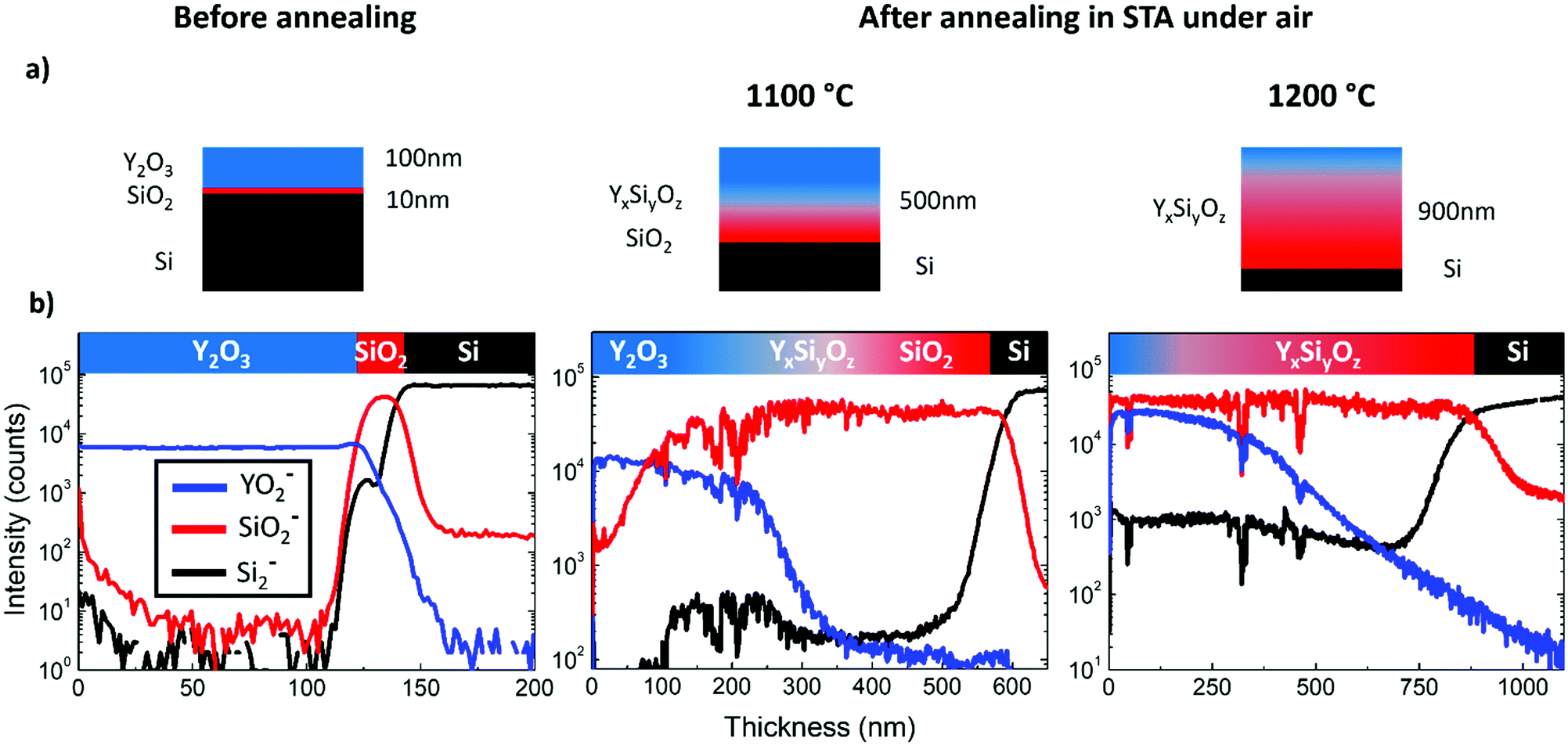 | ||
| Fig. 2 Effect of annealing for a single Eu:Y2O3 thin film grown on (111) Si. (a) Schematic representation of the films’ composition. (b) TOF-SIMS of the sample as-grown and following thermal annealing. The as-grown sample shows a sharp interface between each layer whereas a significant intermixing to form YxSiyOz occurs at high-temperature annealing. | ||
Three distinct and sharp regions can be identified for the as-grown sample: 100 nm of Y2O3, 10 nm of SiO2 and the Si substrate. However, when annealed at high temperature, thickening of the oxide films is observed which is confirmed by the ellipsometry data of Fig. S3 in the ESI.† At an annealing temperature of 1100 °C/1200 °C, a thickness of 500 nm/900 nm had to be sputtered before reaching the Si substrate interface. This significant thickening of oxide layers is the result of oxygen diffusion from the atmosphere through the Y2O3 film and towards the silicon interface, which gradually oxidized the substrate. Indeed, Y2O3 is known to be an ionic conductor at high temperatures with vacancy-assisted oxygen diffusion.38,39 In addition, Si4+ and Y3+ interdiffusion also occurred40–43 leading to intermixing and the formation of an YxSiyOz layer whose thickness increased with the annealing temperature. The exact composition of the new crystalline intermixing phases could not clearly be identified by XRD as the main peak was superimposed with that of the predominant substrate from Si(111).
Since such thermal treatments appear to significantly modify the crystalline environment, we turned to refined optical characterization in order to evaluate if the Eu3+ emission was affected. Room temperature two-dimensional photoluminescence excitation (2D-PLE) map experiments were conducted around the 7F0 → 5D2 europium transition at different excitation wavelengths, while recording the 5D0 → 7F2 emission. The 2D-PLE maps of films annealed at different temperatures are presented in Fig. 3a–c.
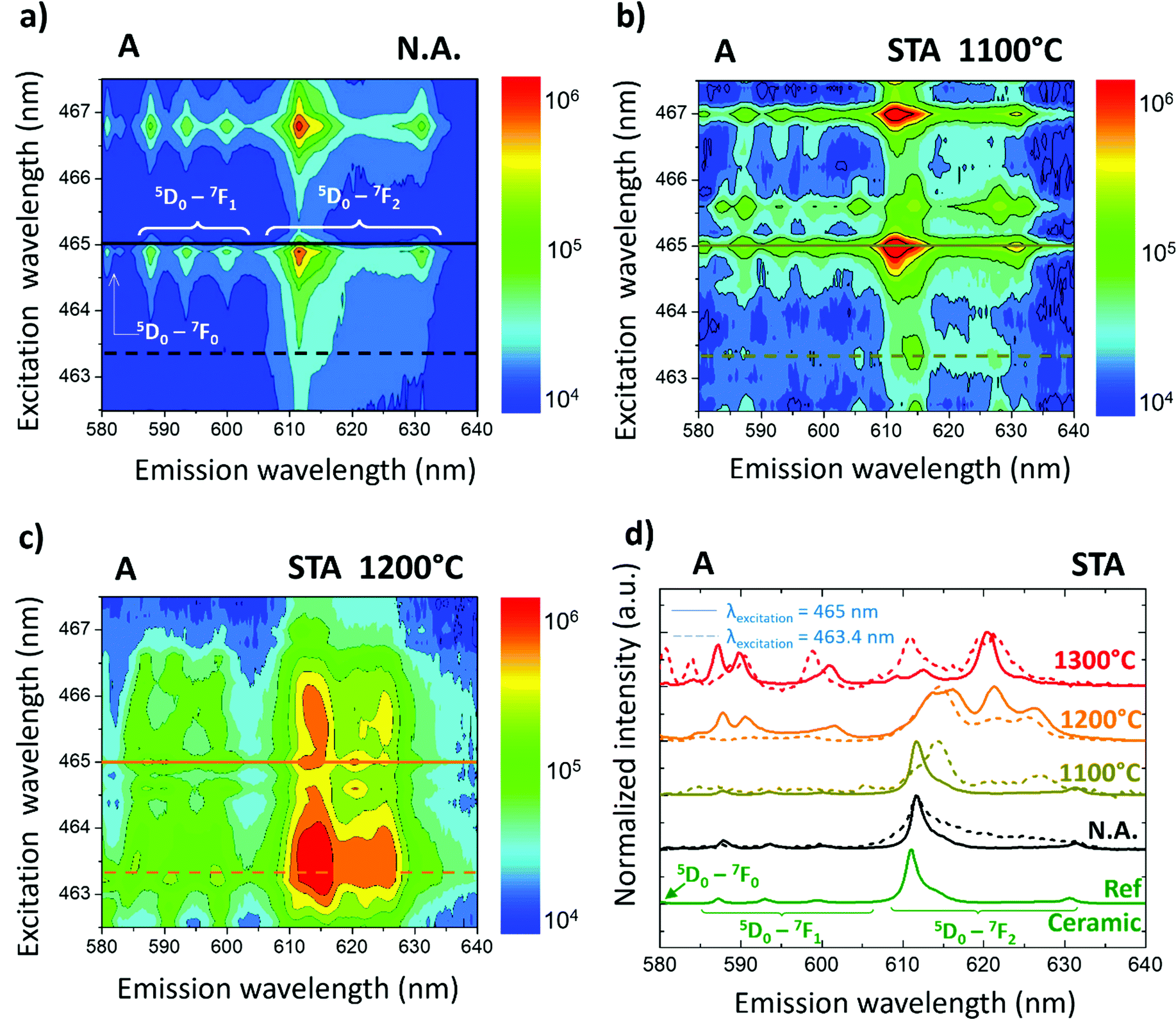 | ||
| Fig. 3 Optical emission at room temperature of the single layer Eu:Y2O3 thin film on Si(111) (labelled A), not annealed (N.A.) and annealed in slow thermal annealing (STA) at various temperatures. (a–c) 2D-PLE maps recorded around the excitation wavelength of the 7F0 → 5D2 Eu transition. Dramatic modification of the emission and excitation is observed after annealing at 1200 °C. The full and dotted lines correspond to the 465 nm and 463.4 nm excitation wavelengths, respectively. The corresponding spectra, normalized to the highest peak intensity, are plotted in (d). A high quality Eu:Y2O3 ceramic spectrum is also shown as a reference. | ||
For the as-grown sample (Fig. 3a), the typical Eu bright and narrow emission centered at 612 nm is observed for excitation wavelengths peaking at 465 and 466.8 nm, which is in good agreement with Eu3+ insertion in the C2 site in cubic Y2O3.44 Moreover, a weak fluorescence also centered at 612 nm is observed for side-line excitation at e.g. 463.4 nm (black dotted line spectrum in Fig. 3d) indicating that some Eu3+ ions experience a slightly distorted environment since the global shape and peak maximum are conserved. The main difference between PL under peak and side-line excitation is an increase of the emission full width at half maximum (FWHM) that is characteristic of a disordered environment. This broader emission has an intensity about twenty times lower in comparison with the bright emission under excitation at 465 nm, indicating that only a minor number of Eu ions experienced a distorted surrounding.
After annealing at 1100 °C, the 2D-PLE map shows slight changes in comparison to the as-grown film (Fig. 3b). For the excitation at 465 nm, a 10% increase of the FWHM emission at 612 nm is observed confirming that the cubic phase presents additional disorder. New weak and relatively narrow emission lines appear e.g. for excitation at 463.4 nm (Fig. 3d, dotted green curve) which likely correspond to new crystalline phases.45–48 However, as the global shape of the 2D-PLE map is conserved, we can conclude that a distorted cubic phase of Y2O3 remains the main crystalline environment experienced by Eu ions.
When the annealing temperature is further increased to 1200 °C (Fig. 3c), new emission peaks between 613 nm and 628 nm become dominant whatever the excitation wavelength and the distortion of the spectra gets stronger. In this case, the change in the 2D-PLE map is dramatic with a strong broadening in both the excitation and emission wavelengths. Indeed, the most intense PL is observed for excitation at 463.4 nm (Fig. 3c) revealing that new phases are now predominant. A further increase of the annealing temperature above 1300 °C leads to a total modification of the 2D-PLE map, indicating complete change of the film's structure (Fig. S4a of the ESI† and full and dotted red lines in Fig. 3d). Those results are in good agreement with the TOF-SIMS analysis: silicon and oxygen diffuse through the sample creating new intermixed phases of silicate (YxSiyO1.5x+2y) as soon as temperatures of 1100 °C are used. For temperatures of 1200 °C and above, the crystalline environment is so drastically changed that the emission is completely modified.
In order to evaluate the effect of the annealing procedure on optical properties, we also measured inhomogeneous linewidth for the single layer film as a function of annealing temperature. The measurements presented in Fig. 4 were done at 10 K by monitoring the 5D0 → 7F2 Eu red emission while the narrow laser line was swept around the central frequency to probe the 7F0 → 5D0 transition (580.88 nm). This low temperature high-resolution excitation measurement is phase and site selective and only Eu ions inserted in the C2 site of the cubic Y2O3 phase are probed.
 | ||
| Fig. 4 Inhomogeneous linewidth at 10 K for the as-grown single Eu:Y2O3 layer on Si(111) (N.A.) and after STA annealing at 1100 °C for 2 h in air. Solid lines are Lorentzian fits to the experimental data, from which the full width at half maximum (FWHM) are extracted. | ||
We found an inhomogeneous linewidth of 40 GHz for the as-grown 2% Eu:Y2O3 thin film which is consistent with a previous study of thin films.35 This value remains broader than for high quality nanoparticles (10 GHz at 0.3% Eu:Y2O3).15 This broadening is attributed to the presence of points or defects especially located close to the substrate's interface.17 Annealing at 1100 °C for 2 h in air more than doubles the linewidth to 96 GHz with a blue shift of the central frequency. This blue shift already reported for ALD films23 is possibly related to the generation of thermal stress due to the thermal expansion coefficient mismatch between silicon and yttria.49,50
The increase of the inhomogeneous linewidth is attributed to disorder that creates nano-scale variations in the ion environment that shift their resonant frequency. We identify two major contributions of disorder: the thermal stress during the annealing post treatment but also the Si4+ diffusion into Y2O3. As the atomic radius of Si4+ is smaller than that of Y3+, its substitution causes strain in the host lattice and changes the crystal field experienced by Eu ions. Moreover, tetravalent Si4+ to trivalent Y3+ substitution requires charge compensation defects (e.g. interstitial oxygen) that also induce a significant change of the crystal field parameter.51 These two combined effects lead to a distribution of excitation wavelengths38 and thus to an increase in the inhomogeneous linewidth.
2. Encapsulation using a multi-layer Y2O3/Eu:Y2O3/Y2O3
In order to keep the curative aspect of annealing while limiting disorder,17,26,30,52 the Eu ions of interest in the active layer were protected with undoped Y2O3 buffer and cap layers of similar thicknesses of 80 nm (Fig. 5a). The encapsulated sample is labelled ABC. It was then annealed in STA in the range of 1100 to 1300 °C for 2 h in air. The 2D-PLE map results are presented below (Fig. 5b).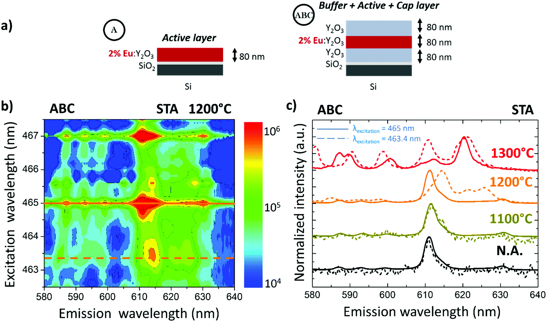 | ||
| Fig. 5 Encapsulation of Eu:Y2O3 by undoped buffer and cap layers. (a) Schematics showing the 2 samples considered here, the first one having an 80 nm-thick active layer of Eu:Y2O3 (A), the other one having the same active layer sandwiched between undoped 80 nm-thin buffer and cap layers (ABC). (b) 2D PLE map for the ABC sample after STA annealing at 1200 °C. The full and dotted lines correspond to the 465 nm and 463.4 nm excitation wavelengths, respectively. The corresponding spectra are plotted in (c) after normalizing to the intensity of the highest peak. | ||
The 2D-PLE map of the multilayer ABC (Fig. 5b) is not as drastically changed as the single layer A after annealing at a temperature of 1200 °C (Fig. 3c). Furthermore, for temperatures lower than 1200 °C, no changes were observed in the emission spectra even when exciting at 463.4 nm where new phases were visible on the single active layer A (dotted green curve). Encapsulating the doped layer seems to have efficiently preserved the active region from silicon diffusion and delayed the formation of an intermixing phase that deteriorates the ions’ environment. However, when annealing at 1300 °C (Fig. S4a in the ESI†) a significant modification of the spectra is once again visible, and the benefit of the multi-layer structure no longer applies.
Since the main origin of the parasitic phase is due to silicon diffusion, a fast post-treatment by RTA for 5 min has also been investigated and the results are presented in the ESI† (Fig. S4b). For the single active layer A, PL results show a strong modification of the Eu emission spectra only for temperatures higher than 1200 °C (Fig. S4b-ii, ESI†), which are 100 °C higher than with STA.
A combination of short annealing time using the RTA system together with multi-layers has also been explored to extend the annealing temperature and try to limit the time available for diffusion into the active layer (see the ESI,† Fig. S4b-ii). Thanks to this approach, we successfully extended the maximal annealing temperature of the multilayer structure up to 1200 °C.
Encapsulating the active layer thus protects the emitting ions from diffusion of Si from the substrate and parasitic phase formation during annealing. To push further the effect of encapsulation, we prepared a final multilayered sample with a 200 nm-thick active layer of Eu:Y2O3 between two other layers of undoped Y2O3 but with a much thicker buffer layer of 2 μm and a 20 nm-thin undoped capping layer. This sample labelled D is presented in the inset of Fig. 6b. We then investigated the effect of post-annealing temperature of all three samples A, ABC and D, using either the STA and RTA, on the inhomogeneous linewidths and peak position (Fig. 6a).
 | ||
| Fig. 6 (a) Inhomogeneous linewidth and position for different post-treatments. NA stands for Not Annealed (in green/empty symbol); STA, slow thermal annealing (in blue/filled symbol); RTA, rapid thermal annealing (in orange, half-filled symbols). Circle symbols for active layers only, square symbols for thin multilayers (buffer, active and cap layers) and star symbol for the thick multilayer. (b) Inhomogeneous linewidth of the as grown thick film (sample D) revealing the lowest broadening of 18 GHz. The red line is a Lorentzian fit to the experimental data. | ||
The as-grown multilayer architecture ABC exhibited an inhomogeneous linewidth between 40 and 50 GHz (green region) comparable to that of a single layer. The thick unannealed sample D however led to an inhomogeneous linewidth of 18 GHz which is the narrowest reported so far for a Eu:Y2O3 thin film to our knowledge. This indicates that localizing the ions away from the reactive substrate interface helped in preserving their properties even before any annealing. After post treatment, inhomogeneous linewidths are clearly broadened by up to a factor of 2 for STA to reach 100 GHz and up to a factor of 4 for RTA to reach 170 GHz. The broadening goes with a systematic shift of the peak position to higher frequencies. This shift remains smaller than 100 GHz (<0.11 nm) and might be due to stress induced by the annealing.3,18 Nevertheless, the use of a multilayer strategy limited the broadening by about 50% as compared to a single layer. For instance, with STA treatment at 1100 °C, sample A has an inhomogeneous linewidth of 96 GHz while the ABC sample only displays 75 GHz (Fig. 6a).
For the RTA treatment, diffusion should however not be a dominant source of broadening due to the short annealing time (5 minutes) and cannot explain the large increase in inhomogeneous linewidth observed. Indeed the fast ramps for heating and cooling led to the build-up of stress and delamination of the layer at the interface has sometimes been observed.53 The film delamination and the large inhomogeneous broadening induced by this treatment led us to rule out this option and to retain the conventional longer duration annealing procedure (STA).
Annealing post treatment of the films broadens ΓIn and shifts the central peak position due to thermal stress and an increased diffusion of Si, O and Y atoms. This led to an intermixing layer especially when the annealing temperature is higher. Nevertheless, as inhomogeneous linewidth is not sensitive to dynamical processes affecting Eu ions, the broadening does not necessarily preclude that individual RE ions exhibit narrow homogeneous lines.1,17 Indeed, the homogeneous line is sensitive to dynamical fluctuations of the environment whereas the inhomogeneous line reveals mainly static perturbations.
In order to get more insight into the coherent properties of the post-annealed single and multi-layered thin film, spectral hole burning (SHB) experiments were performed at 3 K on the A and ABC samples annealed at different temperatures with the STA procedure. SHB is an extremely sensitive optical method that can probe optical homogeneous linewidths (Γhom) and therefore the effect of dynamical fluctuations on RE ion transitions.54,55 Indeed, dynamic changes of the RE ions’ environment modify their optical transition frequencies and induce decoherence. Therefore, the linewidth broadening can be used as an ultra-sensitive probe of fluctuations with different origins like magnetic and charge noise, or dynamical disorder.56,57 Note that as resonant excitation is used, SHB does not probe other ions and phases than Eu ions inserted in the C2 site of the cubic phase of Y2O3.
In this experiment, a spectral hole is burned into the 7F0 → 5D0 inhomogeneous absorption line by using a narrow line dye laser that optically pumps out the population of one long-lived ground state hyperfine level. Afterwards the resulting change in absorption is monitored with the variation of the red fluorescence intensity of the 5D0 → 7F2 transition.54 Indeed, when the optical linewidth of the laser is narrower than the hyperfine splitting (typically tens of MHz for the isotopes 151 and 153 of Eu3+ ions58) the burning pulse changes the population distribution between the hyperfine levels of Eu3+ ions. This population depletion at the burning frequency leads to a reduction of the red fluorescence emission intensity, while at the same time, since the population of the other ground state hyperfine levels increases, brighter fluorescence (anti-holes) may appear on each side of the central hole. The SHB spectrum is recorded by probing the fluorescence contrast for different detuning frequencies between burn and probe pulses. In contrast, when the optical linewidth of the ions is larger than the hyperfine splitting, the population redistribution does not occur, and fluorescence intensity is constant. A more precise description of the measurement, the set-up and the laser sequence are available in a previous publication.35
Spectral hole burning measurements provide information about the Γhom of the optical transition via the width of the spectral hole (Γhole). In the weak excitation limit, the spectral hole width is twice the effective homogeneous linewidth. The effective homogenous linewidth has a temporal dependence too. Indeed, it is a combination of the intrinsic homogeneous linewidth of 5D0 → 7F0 optical transition with broadening induced by faster dephasing processes than the time scale of the measurement. For that reason, effective homogeneous linewidths deduced by SHB measurements are usually broader than that deduced from two pulse photon echoes.
Fig. 7a illustrates the effect of the burning pulse on the fluorescence emission after the probe pulse for the as-grown samples A and ABC, respectively. A different behavior is observed between the two samples. Indeed, for sample A (without buffer layer) no change of the luminescence is observed when using or not a burning pulse. This result indicates that a hole is not burned probably due to a too broad Γhom. In contrast, a significant fluorescence contrast is detected on the ABC sample thereby confirming the validity of the multilayer architecture. The Γhole before any post-treatment is around 23 MHz (blue curve, Fig. 7b). This value is about 10 times larger in comparison to Γhole recorded under the same experimental conditions on Eu doped nanoparticles.17
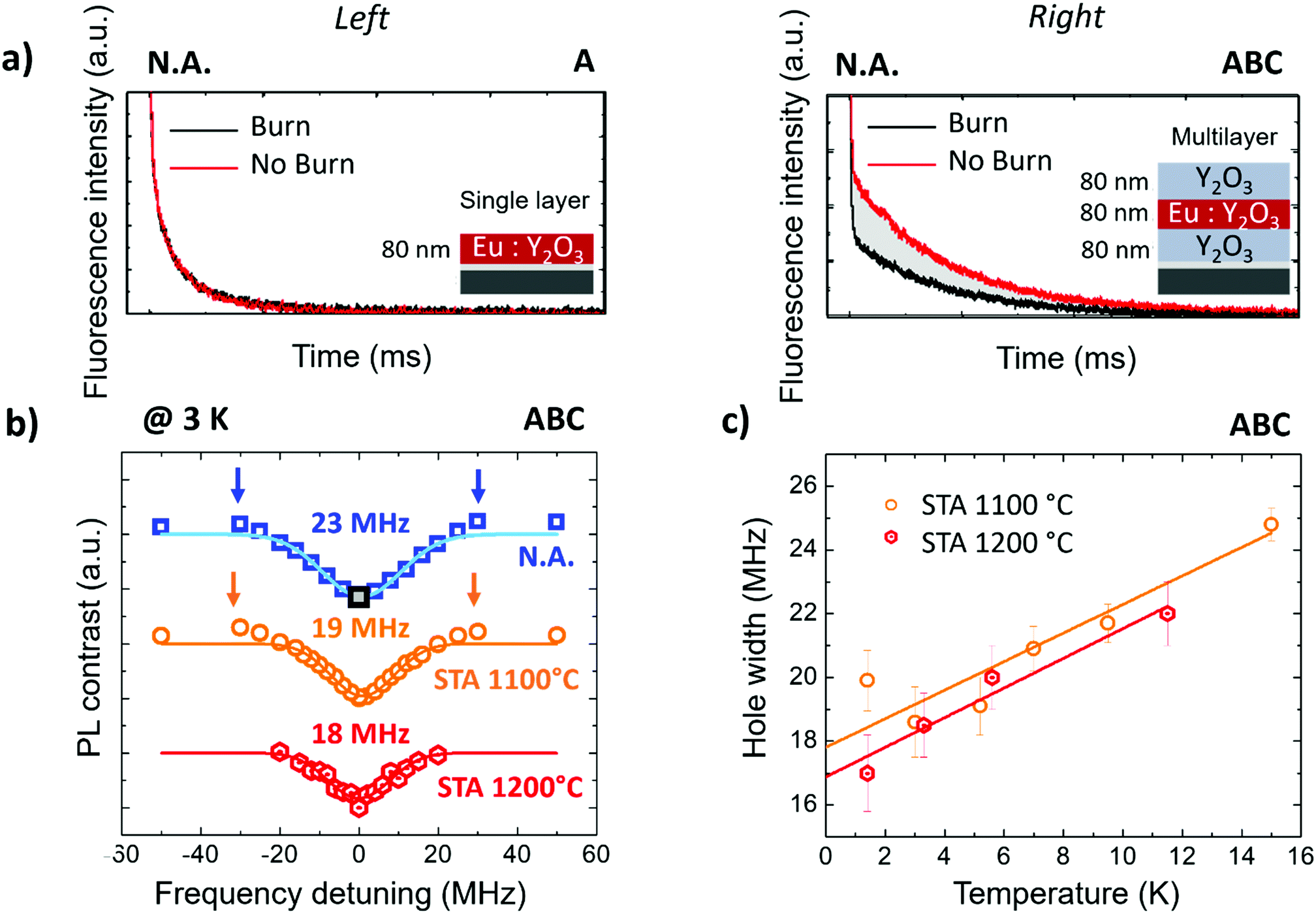 | ||
| Fig. 7 SHB experiment at 3 K for A and ABC samples STA annealed for 2 h at various temperatures in air. (a) PL decay of the 5D0 → 7F2 transition of Eu following the probe pulse used for the as deposited A (left) and ABC (right) samples. A strong PL decrease is only visible for the ABC sample the contrast of which is highlighted in grey and corresponding to the grey square in (b). (b) PL contrast as a function of central frequency detuning revealing a spectral hole in the ABC sample as-grown and after STA annealing. Anti-holes are also visible beside the hole central position (blue and orange arrows). Full lines are Lorentzian fits of the experimental data. (c) Hole width Γhole variation with temperature showing a linear trend. | ||
The effect of the post treatment on the SHB spectra is presented in Fig. 7b for the ABC sample. We observe two modifications of the SHB spectrum with the annealing temperature. For a 1200 °C annealing, a significant decrease of the photoluminescence signal is observed (Fig. 7b) that could be attributed to the formation of mixed Eu doped YxSiyOz phases. In our experiment, the narrow line laser (300 kHz) is extremely selective and only europium ions at 580.88 nm are probed, which corresponds to the cubic Y2O3 phase. Eu3+ ions in other phases are likely to show different transition wavelengths and are not probed. As an example the excitation wavelengths for the two sites of europium in Y2SiO5 are centered at 580.039 nm and at 580.209 nm respectively,59,60 far away from the excitation wavelength of Eu:Y2O3. Secondly, when a post-annealing treatment in STA is applied, the Γhole gets narrower, down to 18 MHz at 1200 °C (Fig. 7b). This indicates that dynamical perturbations are reduced thanks to the thermal treatment. However, that Γhole value remains broad and suggests that additional dephasing processes still occur.
Among the different dephasing mechanisms (e.g. spin flip flops and electric field fluctuations), those related to local disorder, known as Two Level Systems (TLSs), have been reported to have a strong impact on the linewidth of amorphous materials but also on disordered single crystals and nanoparticles.15,61 The origin of this dynamical perturbation is linked to low frequency local disorder modes due to the tunneling of atoms between local configurations of equivalent energies.
We confirm the presence of the TLS dephasing mechanism by probing the evolution of the Γhole as a function of the temperature in Fig. 7c for the ABC sample. Indeed the Γhole increases linearly with temperature, as expected for a TLS process. The slope of broadening is about 0.5 MHz K−1. This value is close to those reported for Eu doped disordered crystals like Ca1−xMxF2+x (1–10 MHz K−1)62 and Eu in Y2−xZrxO3 or Y2−xScxO3 (1 MHz K−1)63 and one order of magnitude lower in comparison to Eu doped silicate glass (10–50 MHz K−1).59,64 This result seems to be in good agreement with the disorder due to the Si4+ diffusion responsible for the broadening of inhomogeneous linewidth. Surprisingly, the slope is similar for annealing at 1100 °C and 1200 °C respectively. Assuming that the coupling of Eu3+ ions to the TLS is the same, this suggests that the TLS density of states is independent of the annealing temperature. A possible explanation might be the saturation of the TLS density of state above a Si4+ threshold. This kind of saturation has already been described in the disordered crystal Ca1−xMxF2+x for a low value of x.63 Moreover, the extrapolated value at 0 K of Γhole (about 17 MHz) remains large in comparison to the bulk, underlying the existence of other dephasing including TLS not related to Si4+ diffusion. Indeed, TLS dephasing has also been observed in Eu:Y2O3 nanoparticles by SHB (0.2 to 0.7 MHz K−1) indicating that additional TLS related to other defects (e.g. oxygen vacancies) might occurred in Y2O3. More SHB results are available in Table S5 in the ESI,† underlining our motivation to work with post-annealed multilayered thin films.
In order to confirm the impact of the Si4+ diffusion on the Γhole we probed the effect of different thermal post treatments on the thicker multilayer device (sample D). For annealing at 1100 °C in air Γhole is slightly reduced to 15 MHz confirming that the encapsulation of the active layer far from the silicon interface reduced the dephasing processes (see Table S5 in the ESI†). One possible explanation of the thick buffer's weak impact could be that the Si4+ still diffuses. Indeed, during air post treatment, the silicon interface remains oxidized and will release Si4+ ions into the buffer layer. For a polycrystalline film, a fast diffusion path along the grain boundaries could still exist. For this reason, we investigated a two-step post-treatment with the aim to reduce the silicon oxidation as far as possible. For that, we performed the 1100 °C annealing under an argon atmosphere rather than air. During this first high temperature annealing no silicon oxidation occurs. Then a second annealing at 600 °C under oxygen was performed to improve the oxygen stoichiometry of the yttria layer while limiting Si diffusion. SHB measurements in Fig. 8 were then performed on this thicker doubly annealed film.
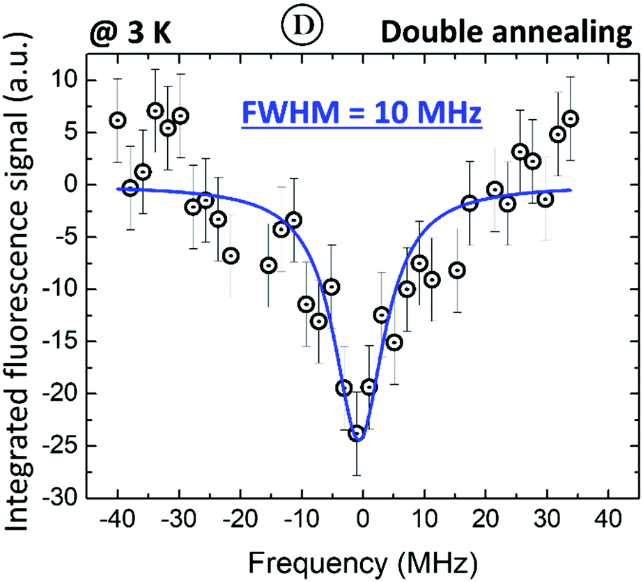 | ||
| Fig. 8 SHB measurements of a 2 μm-thick multilayer sample (labelled D) with 2-step annealing (1100 °C under Ar and 600 °C under O2). Spectral hole burning experiment at 3 K showing a hole width Γhole of 10 MHz. | ||
SHB measurements showed a narrow spectral hole, Γhole of 10 MHz. The effective Γhom deduced is about 5 MHz. This improvement was observed by combining the multi-layer strategy on a thick film and an adapted annealing post-treatment to limit interfacial reactions and Si4+ diffusion.
Conclusions
In this work, we have improved the optical properties of thin RE-doped oxide films grown by DLI-CVD on silicon for scalable optical quantum technologies. The Eu:Y2O3 polycrystalline films grew in a columnar growth mode with full (111)-texture when a thin thermal SiO2 oxide is used between the substrate and the film. Although high-temperature post-annealing treatment is useful to improve the optical properties of the films, it was observed that above a temperature of 1100 °C, Si and Y intermixing as well as oxygen diffusion towards the interface become critical and drastically change the film's phase and RE's environment thus leading to systematic broadening of the inhomogeneous linewidths. To circumvent this issue, we propose the use of a multi-layer strategy in which the active layer containing the emitters’ ions is protected by buffer and cap layers. This helped limiting the inhomogeneous linewidth broadening during annealing by up to about 50% and also reduced the spectral hole width by up to 20%. By pushing this approach further, a double annealing treatment, under different atmospheres, was done to a thicker buffered sample in order to limit as much as possible the formation of these intermixed phases. This led to the narrowest inhomogeneous (18 GHz) and homogeneous (5 MHz) linewidths reported so far in Eu:Y2O3 thin films. Future efforts to reduce Γhom should however be directed to the improvement of the structural quality of our Y2O3 thin films and reduce the presence of grain boundaries as well as impurities and defects that can possibly act as additional sources of decoherence. Nevertheless, this paves the way towards the use of RE ions as a valuable platform for quantum memory devices.Author contributions
The work was conceptualized by N. H., A. T. and A. F. TOF-SIMS experiments were conducted by A. S. and analysed by A. F. TEM experiments were conducted and analysed by X. P. and C. L. All other experiments were conducted by N. H., A. T., D. S. and A. F. and discussed with P. G. All the authors contributed to the final version of the manuscript.Conflicts of interest
There are no conflicts to declare.Acknowledgements
This project has received funding from the European Union's Horizon 2020 Research and Innovation Programme under Grant Agreement No. 820391 (Square). We acknowledge financial support from the Paris network on quantum technologies (SIRTEQ). X. P. and C. L. are grateful to F. Lemarié for the TEM sample preparation. They also thank the ANR (Agence Nationale de la Recherche) for its funding through an EQUIPEX project (Grant ANR-11-EQP-020) and the Normandie Region which allowed the FIB system to be purchased. The authors would like to thank D. De Barros for help in designing the reactor chamber as well as H. Guillon from Kemstream for support with the evaporator system.Notes and references
- C. W. Thiel, T. Böttger and R. L. Cone, J. Lumin., 2011, 131, 353–361 CrossRef CAS.
- D. D. Awschalom, R. Hanson, J. Wrachtrup and B. B. Zhou, Nat. Photonics, 2018, 12, 516–527 CrossRef CAS.
- T. Böttger, C. W. Thiel, R. L. Cone and Y. Sun, Phys. Rev. B: Condens. Matter Mater. Phys., 2009, 79, 115104 CrossRef.
- M. Zhong, M. P. Hedges, R. L. Ahlefeldt, J. G. Bartholomew, S. E. Beavan, S. M. Wittig, J. J. Longdell and M. J. Sellars, Nature, 2015, 517, 177 CrossRef CAS PubMed.
- E. Saglamyurek, J. Jin, V. B. Verma, M. D. Shaw, F. Marsili, S. W. Nam, D. Oblak and W. Tittel, Nat. Photonics, 2015, 9, 83–87 CrossRef CAS.
- N. Lauk, N. Sinclair, S. Barzanjeh, J. P. Covey, M. Saffman, M. Spiropulu and C. Simon, arXiv:1910.04821 [quant-ph].
- A. Kinos, D. Hunger, R. Kolesov, K. Mølmer, H. de Riedmatten, P. Goldner, A. Tallaire, L. Morvan, P. Berger, S. Welinski, K. Karrai, L. Rippe, S. Kröll and A. Walther, arXiv:2103.15743 [quant-ph].
- T. Böttger, C. W. Thiel, Y. Sun and R. L. Cone, Phys. Rev. B: Condens. Matter Mater. Phys., 2006, 73, 075101 CrossRef.
- C. W. Thiel, W. R. Babbitt and R. L. Cone, Phys. Rev. B: Condens. Matter Mater. Phys., 2012, 85, 174302 CrossRef.
- Y. Sun, T. Böttger, C. W. Thiel and R. L. Cone, Phys. Rev. B: Condens. Matter Mater. Phys., 2008, 77, 085124 CrossRef.
- B. Merkel, A. Ulanowski and A. Reiserer, Phys. Rev. X, 2020, 10, 041025 CAS.
- J. M. Kindem, A. Ruskuc, J. G. Bartholomew, J. Rochman, Y. Q. Huan and A. Faraon, arXiv:1907.12161 [quant-ph].
- M. Raha, S. Chen, C. M. Phenicie, S. Ourari, A. M. Dibos and J. D. Thompson, Nat. Commun., 2020, 11, 1605 CrossRef CAS PubMed.
- A. Perrot, Ph. Goldner, D. Giaume, M. Lovrić, C. Andriamiadamanana, R. R. Gonçalves and A. Ferrier, Phys. Rev. Lett., 2013, 111, 203601 CrossRef CAS PubMed.
- J. G. Bartholomew, K. de Oliveira Lima, A. Ferrier and P. Goldner, Nano Lett., 2017, 17, 778–787 CrossRef CAS PubMed.
- D. Serrano, J. Karlsson, A. Fossati, A. Ferrier and P. Goldner, Nat. Commun., 2018, 9, 2127 CrossRef CAS PubMed.
- S. Liu, A. Fossati, D. Serrano, A. Tallaire, A. Ferrier and P. Goldner, ACS Nano, 2020, 14, 9953–9962 CrossRef CAS.
- B. Casabone, J. Benedikter, T. Hümmer, F. Oehl, K. de Oliveira Lima, T. W. Hänsch, A. Ferrier, P. Goldner, H. de Riedmatten and D. Hunger, New J. Phys., 2018, 20, 095006 CrossRef.
- T. Zhong and P. Goldner, Nanophotonics, 2019, 8, 2003–2015 CAS.
- B. Merkel, A. Ulanowski and A. Reiserer, Phys. Rev. X, 2020, 10, 041025 CAS.
- D. Cano, A. Ferrier, K. Soundarapandian, A. Reserbat-Plantey, M. Scarafagio, A. Tallaire, A. Seyeux, P. Marcus, H. de Riedmatten, P. Goldner, F. H. L. Koppens and K.-J. Tielrooij, Nat. Commun., 2020, 11, 4094 CrossRef CAS PubMed.
- K. Xia, F. Sardi, C. Sauerzapf, T. Kornher, H.-W. Becker, Z. Kis, L. Kovacs, R. Kolesov and J. Wrachtrup, arXiv:2104.00389 [cond-mat, physics:physics, physics:quant-ph].
- M. Scarafagio, A. Tallaire, K.-J. Tielrooij, D. Cano, A. Grishin, M.-H. Chavanne, F. H. L. Koppens, A. Ringuedé, M. Cassir, D. Serrano, P. Goldner and A. Ferrier, J. Phys. Chem. C, 2019, 123, 13354–13364 CrossRef CAS.
- X. Xu, V. Fili, W. Szuba, M. Hiraishi, T. Inaba, T. Tawara, H. Omi and H. Gotoh, Opt. Express, 2020, 28, 14448 CrossRef CAS PubMed.
- M. K. Singh, A. Prakash, G. Wolfowicz, J. Wen, Y. Huang, T. Rajh, D. D. Awschalom, T. Zhong and S. Guha, APL Mater., 2020, 8, 031111 CrossRef CAS.
- M. Scarafagio, A. Tallaire, M.-H. Chavanne, M. Cassir, A. Ringuedé, D. Serrano, P. Goldner and A. Ferrier, Phys. Status Solidi A, 2020, 1900909 CrossRef CAS.
- S. Pirandola, B. R. Bardhan, T. Gehring, C. Weedbrook and S. Lloyd, Nat. Photonics, 2018, 12, 724–733 CrossRef CAS.
- S. Dutta, E. A. Goldschmidt, S. Barik, U. Saha and E. Waks, Nano Lett., 2020, 20, 741–747 CrossRef CAS PubMed.
- T. Zhong, J. M. Kindem, J. G. Bartholomew, J. Rochman, I. Craiciu, V. Verma, S. W. Nam, F. Marsili, M. D. Shaw, A. D. Beyer and A. Faraon, Phys. Rev. Lett., 2018, 121, 183603 CrossRef CAS.
- M. Scarafagio, A. Tallaire, K.-J. Tielrooij, D. Cano, A. Grishin, M.-H. Chavanne, F. H. L. Koppens, A. Ringuedé, M. Cassir, D. Serrano, P. Goldner and A. Ferrier, J. Phys. Chem. C, 2019, 123, 13354–13364 CrossRef CAS.
- N. Harada, A. Ferrier, D. Serrano, M. Persechino, E. Briand, R. Bachelet, I. Vickridge, J.-J. Ganem, P. Goldner and A. Tallaire, J. Appl. Phys., 2020, 128, 055304 CrossRef CAS.
- S. Liu, D. Serrano, A. Fossati, A. Tallaire, A. Ferrier and P. Goldner, RSC Adv., 2018, 8, 37098–37104 RSC.
- G. P. Flinn, K. W. Jang, J. Ganem, M. L. Jones, R. S. Meltzer and R. M. Macfarlane, J. Lumin., 1994, 58, 374–379 CrossRef CAS.
- A. Ferrier, N. Harada, M. Scarafagio, E. Briand, J.-J. Ganem, I. Vickridge, A. Seyeux, P. Marcus, D. Serrano, P. Goldner and A. Tallaire, J. Phys. Chem. C, 2020, 124, 19725–19735 CrossRef CAS.
- N. Harada, A. Ferrier, D. Serrano, M. Persechino, E. Briand, R. Bachelet, I. Vickridge, J.-J. Ganem, P. Goldner and A. Tallaire, J. Appl. Phys., 2020, 128, 055304 CrossRef CAS.
- K. Reinhardt, Handbook of silicon wafer cleaning technology, Elsevier, Waltham, MA, 3rd edn, 2018 Search PubMed.
- W. Kern, J. Electrochem. Soc., 1990, 137, 1887–1892 CrossRef CAS.
- K. Ando and Y. Oishi, in Transport in Nonstoichiometric Compounds, ed. G. Simkovich and V. S. Stubican, Springer US, Boston, MA, 1985, vol. 129, pp. 203–215 Search PubMed.
- S.-K. Kang, D.-H. Ko, E.-H. Kim, M. Ho Cho and C. N. Whang, Thin Solid Films, 1999, 353, 8–11 CrossRef CAS.
- D. J. Cherniak, Phys. Chem. Miner., 1998, 26, 156–163 CrossRef CAS.
- C. Legros, B. Lesage, G. Borchardt, M. Kilo and F. Jomard, Defect Diffus. Forum, 2005, 237–240, 432–437 CAS.
- H. Mehrer, Diffusion in Solids: Fundamentals, Methods, Materials, Diffusion-Controlled Processes, Springer-Verlag, Berlin Heidelberg, 2007 Search PubMed.
- L. G. Harrison, Trans. Faraday Soc., 1961, 57, 1191 RSC.
- K. de Oliveira Lima, R. Rocha Gonçalves, D. Giaume, A. Ferrier and P. Goldner, J. Lumin., 2015, 168, 276–282 CrossRef CAS.
- D. den Engelsen, T. G. Ireland, P. G. Harris, G. R. Fern, P. Reip and J. Silver, J. Mater. Chem. C, 2016, 4, 8930–8938 RSC.
- J. Zhang, H. Cui, P. Zhu, C. Ma, X. Wu, H. Zhu, Y. Ma and Q. Cui, J. Appl. Phys., 2014, 115, 023502 CrossRef.
- S. Lu, J. Zhang and J. Zhang, J. Nanosci. Nanotechnol., 2010, 10, 2152–2155 CrossRef CAS PubMed.
- H.-S. Yang, K. S. Hong, S. P. Feofilov, B. M. Tissue, R. S. Meltzer and W. M. Dennis, J. Lumin., 1999, 83–84, 139–145 CrossRef.
- A. M. Stoneham, Proc. Phys. Soc., 1966, 89, 909–921 CrossRef CAS.
- A. M. Stoneham, Rev. Mod. Phys., 1969, 41, 82–108 CrossRef.
- J. B. Gruber, D. K. Sardar, R. M. Yow, B. Zandi and E. P. Kokanyan, Phys. Rev. B: Condens. Matter Mater. Phys., 2004, 69, 195103 CrossRef.
- K. de Oliveira Lima, R. Rocha Gonçalves, D. Giaume, A. Ferrier and P. Goldner, J. Lumin., 2015, 168, 276–282 CrossRef CAS.
- V. Ioannou-Sougleridis, V. Constantoudis, M. Alexe, R. Scholz, G. Vellianitis and A. Dimoulas, Thin Solid Films, 2004, 468, 303–309 CrossRef CAS.
- P. Goldner, A. Ferrier and O. Guillot-Noël, Handbook on the Physics and Chemistry of Rare Earths, Elsevier, 2015, vol. 46, pp. 1–78 Search PubMed.
- M. J. Sellars, R. S. Meltzer, P. T. H. Fisk and N. B. Manson, J. Opt. Soc. Am. B, 1994, 11, 1468 CrossRef CAS.
- R. M. Macfarlane, A. Arcangeli, A. Ferrier and Ph. Goldner, Phys. Rev. Lett., 2014, 113, 157603 CrossRef CAS.
- N. Galland, N. Lučić, B. Fang, S. Zhang, R. Le Targat, A. Ferrier, P. Goldner, S. Seidelin and Y. Le Coq, Phys. Rev. Appl., 2020, 13, 044022 CrossRef CAS.
- W. R. Babbitt, A. Lezama and T. W. Mossberg, Phys. Rev. B: Condens. Matter Mater. Phys., 1989, 39, 1987–1992 CrossRef CAS PubMed.
- R. Yano, M. Mitsunaga, N. Uesugi and M. Shimizu, Phys. Rev. B: Condens. Matter Mater. Phys., 1994, 50, 9031–9034 CrossRef CAS.
- R. W. Equall, Y. Sun, R. L. Cone and R. M. Macfarlane, Phys. Rev. Lett., 1994, 72, 2179–2182 CrossRef CAS.
- G. P. Flinn, K. W. Jang, J. Ganem, M. L. Jones, R. S. Meltzer and R. M. Macfarlane, Phys. Rev. B: Condens. Matter Mater. Phys., 1994, 49, 5821–5827 CrossRef CAS PubMed.
- R. S. Meltzer, K. W. Jang, K. S. Hong, Y. Sun and S. P. Feofilov, J. Alloys Compd., 1997, 250, 279–286 CrossRef CAS.
- K. W. Jang and R. S. Meltzer, Phys. Rev. B: Condens. Matter Mater. Phys., 1995, 52, 6431–6439 CrossRef CAS.
- Th. Schmidt, R. M. Macfarlane and S. Völker, Phys. Rev. B, 1994, 50, 15707–15718 Search PubMed.
Footnote |
| † Electronic supplementary information (ESI) available. See DOI: 10.1039/d1ma00753j |
| This journal is © The Royal Society of Chemistry 2022 |