 Open Access Article
 This Open Access Article is licensed under a
 Creative Commons Attribution 3.0 Unported Licence
Low temperature (Zn,Sn)O deposition for reducing interface open-circuit voltage deficit to achieve highly efficient Se-free Cu(In,Ga)S2 solar cells†
Mohit
Sood
 *a,
Damilola
Adeleye
a,
Sudhanshu
Shukla
a,
Tobias
Törndahl
b,
Adam
Hultqvist
b and
Susanne
Siebentritt
a
*a,
Damilola
Adeleye
a,
Sudhanshu
Shukla
a,
Tobias
Törndahl
b,
Adam
Hultqvist
b and
Susanne
Siebentritt
a
aLaboratory for Photovoltaics, Department of Physics and Materials Science, University of Luxembourg, Belvaux, L-4422, Luxembourg. E-mail: mohit.sood@uni.lu
bSolar Cell Technology, Department of Materials Science and Engineering, Uppsala University, Uppsala, 751 21, Sweden
First published on 13th June 2022
Abstract
Cu(In,Ga)S2 holds the potential to become a prime candidate for use as the top cell in tandem solar cells owing to its tunable bandgap from 1.55 eV (CuInS2) to 2.50 eV (CuGaS2) and favorable electronic properties. Devices above 14% power conversion efficiency (PCE) can be achieved by replacing the CdS buffer layer with a (Zn,Mg)O or Zn(O,S) buffer layer. However, the maximum achievable PCE of these devices is limited by the necessary high heating temperatures during or after buffer deposition, as this leads to a drop in the quasi-Fermi level splitting (qFLs) and therefore the maximum achievable open-circuit voltage (VOC). In this work, a low-temperature atomic layer deposited (Zn,Sn)O thin film is explored as a buffer layer to mitigate the drop in the qFLs. The devices made with (Zn,Sn)O buffer layers are characterized by calibrated photoluminescence and current–voltage measurements to analyze the optoelectronic and electrical characteristics. An improvement in the qFLs after buffer deposition is observed for devices prepared with the (Zn,Sn)O buffer deposited at 120 °C. Consequently, a device with a VOC value above 1 V was achieved. A 14% PCE is externally measured and certified for the best solar cell. The results show the necessity of developing a low-temperature buffer deposition process to maintain and translate absorber qFLs to device VOC.
Introduction
Realizing power conversion efficiency (PCE) above 30% using tandem solar cells needs high-efficiency high bandgap ∼1.5–1.7 eV solar cells to couple with the current state-of-the-art low bandgap solar cells, namely Si, Cu(In,Ga)Se2.1,2 Cu(In,Ga)S2 can fulfill the role of the top cell as it possesses a bandgap (EG) which is tunable from 1.55 eV (CuInS2) to 2.5 eV (CuGaS2),3 which can be tuned to perfectly match the bandgap needed to pair with the bottom solar cell, together with suitable electronic properties. The 15.5% PCE of state-of-the-art Cu(In,Ga)S2 further shows the promise of the material.4 However, the open-circuit voltage (VOC), which is the difference between the electron Fermi level at the front contact and the hole Fermi level at the back contact, is significantly lower (∼340 mV) than the maximum achievable Shockley–Queisser VOC (ref. 5) in the best device. Significant inroads must be made to improve the VOC of Cu(In,Ga)S2 to deploy it as a top cell.In general, achieving a high VOC in a solar cell requires high quasi-Fermi level splitting (qFLs) inside the absorber. Since the qFLs depends majorly on the minority Fermi level under low excitation conditions, high qFLs require significant suppression of non-radiative recombination centers in the bulk of the absorbers.6 Once a good qFLs is ensured, the next step is to properly translate the qFLs into VOC.
Improving the VOC of Cu(In,Ga)S2 solar cells
Chalcopyrite solar cells comprise a complex multi-layered structure (Mo/Cu(In,Ga)S2/buffer/i-layer/Al:ZnO), resulting in many interfaces. Any of these interfaces can be a source of a significant reduction in either or both the electron and hole Fermi-levels, thus reducing the VOC of the final device. This results in an interface VOC deficit, an important metric to quantify the transport loss in the device, which is defined as the difference between the optically measured qFLs/e of the device and the electrically measured VOC of the device.7 Several factors can lead to interface VOC deficit; the most common ones are – (i) unfavorable band-offsets at the various interface and (ii) a high density of defects near the interface.A negative conduction band offset at the absorber/buffer interface is the most common source of interface VOC deficit. The Cu-poor Cu(In,Ga)S2 devices prepared with a CdS buffer layer have been known to suffer from interface VOC deficit8 owing to a negative conduction band offset (CBO) or ‘cliff’ at the absorber/buffer interface, i.e. the conduction band minimum (CBM) energy of the absorber being higher than the conduction band minimum of the buffer.9 The presence of the cliff-type CBO at the Cu(In,Ga)S2/CdS interface results in an interface bandgap that is lower than the bulk bandgap. Consequently, the activation energy (Ea) of the dominant recombination current is less than the EG of the absorber.8 This causes recombinations at the absorber/buffer interface to dominate, and the electron Fermi-level drops at the interface. Hence the VOC is significantly reduced in comparison to the qFLs/e (‘e’ is the elementary charge), causing an interface VOC deficit in the device.
Replacement of the traditional CdS buffer layer with an alternate buffer layer, such as Zn(O,S) and ZnMgO, with a higher CBM is a proven solution to mitigate the interface VOC deficit due to a cliff-type CBO.8,10 However, caution must be exercised when making devices with higher CBM buffer layers. The standard CdS buffer layer is known to already have a cliff-type CBO with the ZnO i-layer.11 And replacing it with a higher CBM buffer would result in an even larger conduction band cliff at the buffer/i-layer interface. For example, we recently studied CIGSu devices prepared with varying Mg content in (Zn,Mg)O films as a buffer layer paired with a ZnO i-layer.10 The (Zn,Mg)O films are known to have a higher CBM than that of ZnO, which increases with increasing Mg content in the films.12 It was found that devices having a high Mg content and, therefore, a large cliff type CBO at the buffer/i-layer interface display a higher interface VOC deficit compared to devices prepared with low Mg content, i.e. with a lower negative CBO at the interface.10 The deficit originates due to a drop in the electron potential near the buffer/i-layer interface, as observed in numerical simulations.10 The loss can be reduced by substituting the ZnO i-layer with a higher CBM i-layer. For example, it has been shown that ZnMgO buffer devices made with an Al:ZnMgO i-layer possess a significantly lower interface VOC loss compared to those of ZnO i-layer devices.10
Besides the negative CBOs at the various interface, a high density of defects inside the absorber near the interface can be another source of the interface VOC deficit in Cu(In,Ga)S2 devices. Sulfide as well as selenide based Cu(In,Ga)S(e)2 solar cells realized with an as grown Cu-rich absorber – overall [Cu]/[In + Ga] > 1 – are known to possess high interface VOC deficits even with perfect band alignment at the absorber/buffer and buffer/i-layer interfaces.13,14 This deficit has been linked to the presence of a high density of acceptor defects near the absorber/buffer interface.7,15 These defects near the interface act as non-radiative recombination centers and therefore cause a drop in the electron Fermi-level near the absorber/buffer interface.7 Consequently, the devices suffer from low VOC and, hence, an interface VOC deficit.
The near interface defect formation has been linked to the etching of the Cu2−xS(e) secondary phase that is necessary for working devices, independent of the etchant used.7,16 The interface VOC deficit due to near interface defects could be somewhat mitigated by doing an S or Se post-deposition treatment after the etching or avoided by making devices using Cu-poor absorbers – [Cu]/[In + Ga] < 1![[thin space (1/6-em)]](https://www.rsc.org/images/entities/char_2009.gif) 14,15,17 – making the etching step unnecessary.
14,15,17 – making the etching step unnecessary.
Therefore, the qFLs/e translation in chalcopyrite solar cells can be hampered by recombinations occurring at or near the absorber/buffer interface or the buffer/i-layer interface.14 It must be noted that the interface VOC deficit can also originate from the molybdenum/absorber interface. However, this is something that is not commonly observed in Cu(In,Ga)S2 devices.
The deposition processes of the buffer, i-layer, or window, when performed at elevated temperatures, can damage the absorber and lead to qFLs loss and consequently result in a lower VOC and, therefore, a global interface VOC deficit. In our recent work, though a device with PCE > 15% could be achieved using a Zn(O,S) buffer layer, the device still possessed an interface VOC deficit of ∼40 mV. It was found that the deficit originates due to a loss in the qFLs after the necessary air annealing of the absorber/buffer stack at ∼200 °C. This annealing is necessary as devices with high PCE are only realized after air annealing the absorber/buffer stack at ∼200 °C.14
Thus, achieving higher VOC values in Cu(In,Ga)S2 solar cells requires mitigation of the above-discussed losses. This can be achieved by using absorbers with a good surface, i.e. Cu-poor Cu(In,Ga)S2 films, an alternate buffer layer that has an optimum CBO (0.0 eV to 0.40 eV) with the absorber,18 and an i-layer that has a suitable CBO with the buffer. In addition, the buffer and i-layer film should not require high temperatures during or after deposition.
The record Cu(In,Ga)S2 device has been achieved using an atomic layer deposited (ALD) Zn1−xMgxO buffer.4 Motivated by this fact, we recently explored the ALD Zn1−xMgxO buffer layer deposited at 150 °C as an alternate to the Zn(O,S) buffer layer for Cu(In,Ga)S2 solar cells, with EG ∼ 1.6 eV.10 A high VOC ∼ 943 mV and a PCE ∼ 14% were achieved using an x = 0.27 Zn1−xMgxO buffer layer. However, even this device exhibited a VOC which was 40 mV lower than the qFLs of the bare absorber. This deficit is partly due to the loss in the qFLs that originated from the ∼150 °C temperature required for buffer deposition, which is still detrimental to device optoelectronic properties, and the rest to the contact loss.10
ALD (Zn,Sn)O is another promising buffer layer and has helped to achieve a VOC of 1 V for CuGaSe2 devices.19 Other than this, the (Zn,Sn)O buffer grown at low temperature of 90–125 °C is known to produce high PCE Cu(In,Ga)Se2 solar cells.19,20 Moreover, the CBM of ALD (Zn,Sn)O can be tuned either by keeping the composition fixed and varying the deposition temperature20 or keeping the deposition temperature fixed and varying the [Sn]/([Zn + Sn]) composition.21
In this work, we explore the impact of an atomic layer deposited (ALD) zinc tin oxide (Zn,Sn)O buffer layer deposited at two different temperatures, 105 °C and 120 °C (keeping the composition constant), as a partner for Cu-poor Cu(In,Ga)S2 solar cells. The benefit of the low growth temperature ≤ 120 °C on the Cu-poor Cu(In,Ga)S2 devices’ properties, particularly the interface VOC deficit, is explored. Moreover, a variety of i-layers, namely ZnO, Al:ZnMgO, and no i-layer at all, are used as a partner for the buffer layer. The resulting devices’ electrical characteristics are measured using current–voltage and external quantum efficiency measurements of the solar cells. Calibrated photoluminescence measurements are performed on the bare absorber and buffer coated absorbers to obtain the qFLs values. The extracted VOC values are compared to the qFLs/e values measured on the bare absorber, and the interface VOC deficits are compared for the different devices. The results presented show that a low-temperature ALD ZnSnO buffer layer with an Al:ZnMgO i-layer can help attain a high PCE in Cu(In,Ga)S2 devices with an interface VOC deficit comparable to those of the state-of-the-art Cu(In,Ga)Se2 devices.22
Experimental
Absorber deposition
The Cu-poor Cu(In,Ga)S2 absorbers were prepared on molybdenum coated soda-lime glass substrates via a 3-stage co-evaporation process at a temperature of ∼570 °C with a final film thickness of ∼2 μm. The desired absorber stoichiometry was obtained by controlling the evaporation flux of the Cu, In, and Ga sources and the durations of the three stages of the process. The final bulk compositions of the as-grown absorbers were determined using energy-dispersive X-ray spectroscopy (EDX). The as-deposited absorbers used in this study had a [Cu]/[In + Ga] ∼ 0.94 and a [Ga]/[Ga + In] ∼ 0.14.Buffer deposition
The Zn1−xSnxOy buffer layer deposition was carried out in an F-120 Microchemistry system using diethyl zinc (DEZ), tetrakis(dimethylamino)tin (TDMASn) and DI water (as a co-reactant) as precursors, with N2 as the carrier and purge gas. A super-cycle approach with a fixed ZnO:SnOx pulse ratio of 1:1 at two different deposition temperatures, 105 °C and 120 °C, was used to deposit (Zn,Sn)O. The buffers at 120 °C were deposited with a total of 750 cycles, whereas the buffers at 105 °C used 938 cycles to compensate for a lower growth per cycle value. The x-values were measured to be 0.19 at 105 °C and 0.18 at 120 °C by X-ray fluorescence on corresponding soda-lime glass pieces placed in the reactor together with the Cu(In,Ga)S2 samples in each run. Throughout this work, the buffers deposited at 105 °C and 120 °C are denoted as B1 and B2, respectively.
i-layer and window layer deposition
The ZnO and Al:ZnMgO i-layer and Al:ZnO window layer deposition was carried out using magnetron sputtering. The sputtering process for Al:ZnMgO was based on a previous work on ZnMgO.18 The 2-inch undoped ZnO target at 125 W and 2-inch 2 wt% Al2O3 doped ZnO target at 140 W were sputtered to deposit i-ZnO and Al:ZnO layers, respectively. Whereas, for depositing Al:Zn1−xMgxO with the desired composition of x = 0.25, 2-inch targets of MgO with 2 wt% Al2O3 and (undoped) ZnO were co-sputtered at a power of 80 W and 110 W, respectively. All the layers were deposited at 1.0 mTorr argon (99.99%) partial pressure, which was maintained with the help of a mass flow controller.After i-layer and window deposition, using e-beam evaporation, nickel and aluminum metal grids were deposited on the samples to complete the device fabrication process. Devices of area ∼0.5 cm2 were realized by mechanical scribing. On the best device, an anti-reflective coating (ARC) of MgF2 was deposited using e-beam evaporation.
Characterization methods
EDX with an operating voltage of 20 kV was used for determining the bulk stoichiometry of the as-grown absorbers. As for buffer thickness and stoichiometry measurements, fused silica glass was used, which was placed in each run as a witness sample. The thicknesses of the (Zn,Sn)O layers were estimated by X-ray reflectivity measurements and the stoichiometry using EDX measurements performed at 20 kV.The qFLs measurements were done using calibrated photoluminescence (PL) using the procedure described in our previous work.23 The VOC measurements and J–V properties were measured using a xenon short-arc lamp AAA-Standard solar simulator together with an IV source-measure unit. The simulator was calibrated to air mass 1.5 global using a Si reference cell. The devices were measured in the forward sweep direction from −0.5 V to 1.5 V with a sweep speed of 50 mV s−1. For determining the external quantum efficiency (EQE) of the devices, a setup consisting of halogen and xenon lamps, a grating monochromator, a chopper, and calibrated reference diodes was used. The current was measured using a lock-in amplifier and the intensity of the light by calibrated reference diodes.
Results and discussion
Fig. 1 shows the one sun-calibrated PL spectra of devices before and after buffer deposition. Among the two buffer layers, the (Zn,Sn)O buffer layer deposited at 120 °C (B2) leads to a very minute deterioration in the PL signal of the device. In contrast, the buffer deposited at 105 °C (B1) leads to a one-order of magnitude drop in the PL signal. Consequently, the qFLs/e drops by 49 mV for the B1 device and 11 mV for the B2 device compared to the bare absorbers.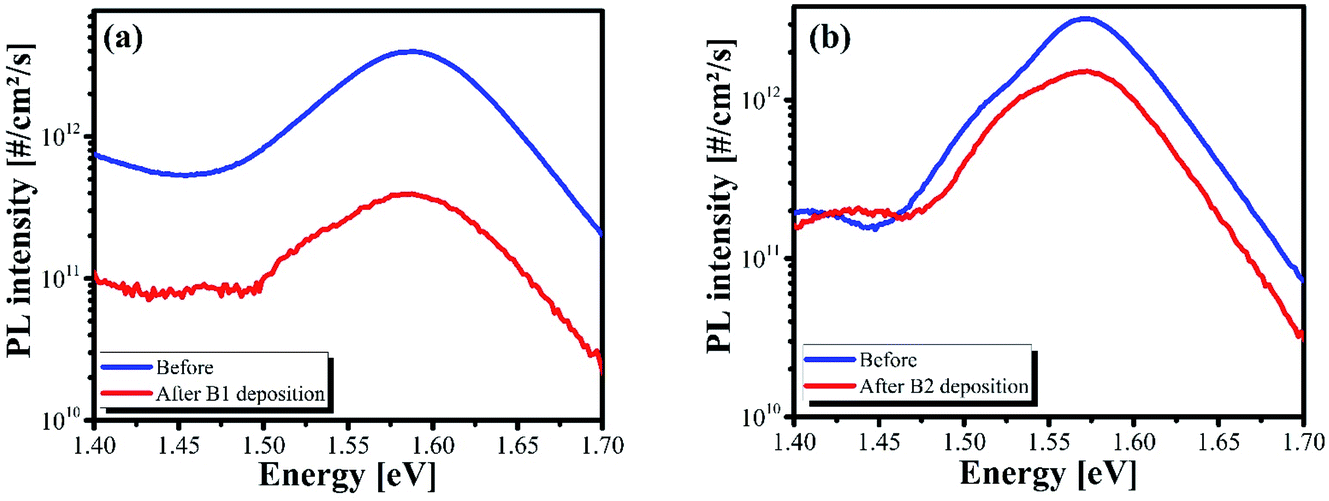 | ||
| Fig. 1 (a) Absolute calibrated photoluminescence spectra of Cu(In,Ga)S2 before and after (Zn,Sn)O buffer layer was deposited at (a) 105 °C (B1) and (b) 120 °C (B2), measured at an illumination intensity equivalent to one sun. | ||
Fig. 2a shows the J–V characteristic curves of the best devices prepared with a (Zn,Sn)O buffer layer deposited at either 105 °C (B1) or 120 °C (B2), shown by dotted and solid lines, respectively. The corresponding electrical characteristic values are reported in Table 1. The PCEs of the devices were obtained by using the following expression:
| PCE = JSC × VOC × FF/Pin, |
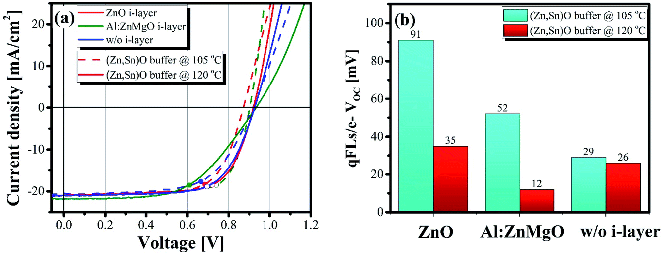 | ||
| Fig. 2 (a) The characteristic J–V curves of the Cu(In,Ga)S2 devices prepared with (Zn,Sn)O buffer layers deposited at 105 °C (B1) and 120 °C (B2), represented by dashed and solid lines respectively. The devices prepared with ZnO, Al:ZnMgO and without an i-layer are represented by red, green and blue lines, respectively. (b) Interface VOC deficit bar plot of devices made with B1 and B2 with various i-layer combinations. | ||
| Buffer layer | i-layer | PCE (%) | FF (%) | J SC (mA cm−2) | V OC (mV) | qFLs/e @1 sun (mV) | qFLs/e − VOC (mV) | R s (Ω cm2) | R sh (Ω cm2) |
|---|---|---|---|---|---|---|---|---|---|
| ZnSnO 105 °C | ZnO | 12.6 | 68.4 | 21.1 | 872 | 963 | 91 | 3.3 | 730 |
| ZnSnO 105 °C | Al:ZnMgO | 13.7 | 73 | 21.0 | 902 | 954 | 52 | 1.3 | 831 |
| ZnSnO 105 °C | W/o | 11.8 | 62.3 | 20.6 | 917 | 946 | 29 | 4.5 | 303 |
| ZnSnO 120 °C | ZnO | 13.3 | 69 | 21.0 | 920 | 955 | 35 | 2.0 | 800 |
| ZnSnO 120 °C | Al:ZnMgO | 11.2 | 55 | 21.9 | 932 | 944 | 12 | 9.8 | 2232 |
| ZnSnO 120 °C | W/o | 13.2 | 67.7 | 21.0 | 926 | 952 | 26 | 3.0 | 1141 |
Among the B1 devices, the device without an i-layer yields the highest VOC and consequently possesses the lowest interface VOC deficit, followed by the Al:ZnMgO i-layer device and the ZnO i-layer device (see Fig. 2b). However, the device without an i-layer exhibits the worst PCE. This is because the device has a significantly lower fill factor (FF) than those of the Al:ZnMgO and ZnO i-layer devices. On the other hand, the Al:ZnMgO i-layer device exhibits the highest FF and a relatively low interface VOC deficit compared to those of the ZnO i-layer device among the three B1 devices. The device thus possesses the highest PCE of ∼ 13.7% among the devices prepared in this study (see Table 1).
To contemplate why the three B1 devices have different FF, the light J–V curves of the device were fitted with the one-diode model using the J–V routine to extract the series and shunt resistance of the device.24 The values are reported in Table 1. The B1 device without an i-layer has a significantly higher series resistance Rs (4.5 Ω cm2) than the B1 devices with a ZnO (2.3 Ω cm2) or Al:ZnMgO (1.3 Ω cm2) i-layer (see Table 1). This trend is in line with the FF observations for the devices, suggesting that the FFs of the device without an i-layer and the ZnO i-layer device are limited primarily due to the high Rs in the devices.
Apart from the high Rs, the low FF of the device without an i-layer also results partly from the low shunt resistance Rsh (303 Ω cm2). This could have possibly originated from the sputter deposition of highly conductive Al:ZnO directly on top of the buffer.25–27 It is possible that the buffer is easily damaged during the sputtering. Hence, during Al:ZnO deposition, the highly conductive window layer comes directly into contact with the absorbers, or worse, with the back contact, resulting in shunting pathways in the device. Therefore, these results suggest that B1 does not provide adequate protection from sputter damage.
As for B2 devices, the Al:ZnMgO i-layer device remarkably exhibits a VOC value of 932 mV, the highest among all the devices prepared in this study. Consequently, it has an interface VOC deficit of a mere 12 mV (see Table 1), which is on par with those of the state-of-the-art Cu(In,Ga)Se2 devices.22 When compared to B1 devices with the same i-layer, the B2 devices exhibit a higher VOC, thus, a lower interface VOC deficit value than their counterparts (see Fig. 2b). This suggests that B2 provides better protection against absorber qFLs loss during the i-layer and window deposition processes. The better protection may be related to the fact that ALD deposited (Zn,Sn)O films grown at higher temperatures with similar compositions are known to be characterized with denser morphologies.28
Unexpectedly, the device with an Al:ZnMgO i-layer performs the worst among this lot. If not for the poor FF, the device would have PCE ∼ 15% without the ARC coating (assuming a similar FF value of 73%, as achieved with the B1 Al:ZnMgO device). Since devices with another batch of absorbers (not shown here) display significantly higher FFs, we treat this as an outlier.
Among all B2 devices, the ZnO i-layer device has the highest PCE ∼ 13.3%. The device displays a 50 mV improvement in the VOC compared to the B1 ZnO i-layer device, and hence a low interface VOC deficit in the device of ∼35 mV. Consequently, it has a 0.7% gain in absolute PCE when compared to the B1 ZnO i-layer device.
The device without an i-layer performs equally well as the ZnO i-layer B2 device. This device also shows significant improvement when compared to the B1 device made without an i-layer. While the interface VOC deficit remains nearly the same, it is the FF in B2 without the i-layer device that makes all the difference. As is evident from Table 1, the absolute FF improves by 5.4%, which can be attributed to a lower Rs value of ∼3.0 Ω cm2 and a significantly higher Rsh value of ∼1141 Ω cm2 as compared to an Rs value of 4.5 Ω cm2 and Rsh value of 303 Ω cm2 in the B1 device. In fact, all the B2 devices possess Rsh values higher than those of the B1 devices. This is a direct indication that B2 provides better protection from any sputter-induced damage to the junction. B2 being deposited at a higher temperature might be the reason for it, as it is less amorphous than B1. Consequently, devices made with it could be less prone to sputter damage during the sputtering of the i-layer and window layer, hence possessing higher VOC, FF and PCE.
To achieve an even higher PCE from the best device obtained in this study, i.e. the Al:ZnMgO i-layer device with B1, it was covered with 110 nm MgF2 ARC coating to decrease the optical losses observed in EQE (Fig. S3†). The device was certified to have a PCE of 13.98 ± 0.39% by the Fraunhofer Institute for Solar Energy Systems. The PCE was obtained by calculating the ratio of maximum-power out from the device to the power-in from solar simulation, i.e. one sun. A different procedure was used as the device displayed different current–voltage I–V curves when measured in the forward (negative to positive) and backward (positive to negative) applied voltage directions (see Fig. 3). Transient I–V characteristics were measured until stable voltage, current, and power values were reached (see Fig. S4†). This power-point was then used as the maximum power-point to calculate the PCE of the device. The device had a measured VOC of 911.8 ± 9.2 mV and 908.9 ± 9.1 mV, an ISC of 9.71 ± 0.18 mA and 9.70 ± 0.18 mA and a FF of 72.31% and 69.93% in the forward and reverse measurement directions, respectively, after obtaining a stable maximum power-point.
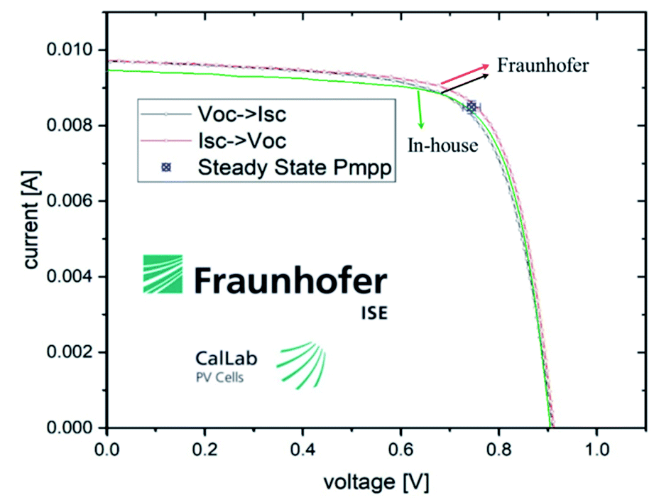 | ||
| Fig. 3 Cu(In,Ga)S2/(Zn,Sn)O/Al:ZnMgO/Al:ZnO certified I–V curves of the 14.0% efficiency device measured at the Fraunhofer Institute for Solar Energy Systems. The red curve is the measurement from the short-circuit current to the external open-circuit voltage, and the black curve is the measurement from the external open-circuit voltage to the short-circuit current. The olive curve is the in-house measurement. The blue square point shows the steady-state maximum power-point of the device achieved by keeping the device at Vmpp for 5 minutes. | ||
Towards 1 V VOC using a thicker buffer
We have previously observed that the density of the buffer has a major impact on the qFLs loss, thus, it is reasonable to assume that the thickness might also have a significant impact on the qFLs value. Therefore, we also explored the impact of the (Zn,Sn)O B2 buffer thickness (by varying the total ALD cycles) on the qFLs of the absorber. Five different numbers of cycles were used – 350, 550, 750, 1000, and 1250 cycles.Fig. 4a shows the variation in the qFLs as a function of the total (Zn,Sn)O buffer ALD cycles. The qFLs loss decreases with increasing ALD cycles and even increases for the device with 1250 buffer cycles . A thicker buffer or mild annealing at 120 °C might be the origin of this improvement.
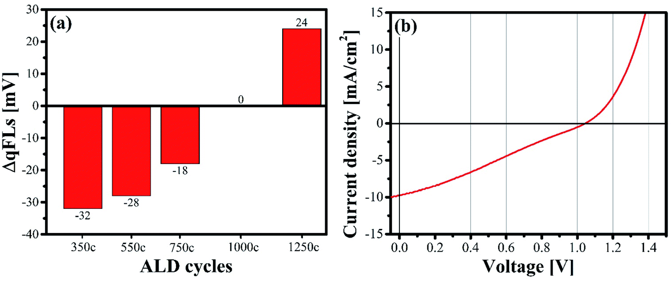 | ||
| Fig. 4 (a) Bar chart showing the change in the qFLs of Cu(In,Ga)S2 absorber before and after buffer deposition as a function of the (Zn,Sn)O buffer thickness. (b) The characteristic J–V curve of the Cu(In,Ga)S2 device prepared with a50 nm thick (Zn,Sn)O buffer layer deposited at 120 °C. | ||
Cu(In,Ga)S2 absorbers grown with high Ga in the first stage of the three-stage growth process with a bandgap of 1.61 eV possess qFLs values higher than 1 eV (obtained from the band to band transition of the PL spectrum).29 Devices prepared using these absorbers together with the optimized buffer thickness resulted in a device VOC value of ∼1.04 V (see Fig. 4b). However, the device possessed poor FF and JSC values and consequently had a mere 2.5% PCE. Nonetheless, the fact that we could achieve VOC values above 1 V is very promising and gives us hope that a PCE above 16% can be achieved provided that VOC values above 1 V can be maintained together with FF values above 73% and JSC values above 22 mA cm−2. This could be a major breakthrough for Cu(In,Ga)S2 solar cells.
Conclusions
The present work shows that by using a (Zn,Sn)O buffer layer deposited at temperatures of ∼120 °C, interface VOC deficit values on par with those of state-of-the-art Cu(In,Ga)Se2 devices can be achieved. This breakthrough was achieved by using a lower buffer deposition temperature compared to our previous work, where 150 °C was used and a higher interface VOC deficit was observed.10 Our results also suggest that the buffer should be dense enough to protect against absorber degradation and sputter damage, which would otherwise lead to a higher interface VOC deficit and low FF in the device. Even though the (Zn,Sn)O buffer layer deposited at temperatures of ∼105 °C resulted in a certified device with PCE of 14%, the buffer process also led to a higher interface VOC deficit. We speculated that this could have resulted from the low density of the (Zn,Sn)O buffer.In addition to these results, we also found that the interface VOC deficit is also dependent on the i-layer used in combination with the buffer, highlighting the importance of the i-layer in the device.
Overall, this work demonstrates that a low interface VOC deficit and, consequently, a high VOC, together with high PCE, can be achieved using Cu(In,Ga)S2 solar cells with a low-temperature (Zn,Sn)O buffer and Al:ZnMgO i-layer.
Conflicts of interest
The authors declare that there is no conflict of interest.Acknowledgements
The authors acknowledge that this research was funded in whole, or in part, by the Luxembourg National Research Fund (FNR), in the framework of the MASSENA project (grant reference [PRIDE 15/10935404]). For the purpose of open access, the author has applied for a Creative Commons Attributions 4.0 International (CC BY 4.0) license to any Author Accepted Manuscript version arising from this submission.References
- A. Onno, N. Rodkey, A. Asgharzadeh, S. Manzoor, J. Y. Zhengshan, F. Toor and Z. C. Holman, Joule, 2020, 4, 580–596 CrossRef CAS.
- G. E. Eperon, M. T. Hörantner and H. J. Snaith, Nat. Rev. Chem., 2017, 1, 0095 CrossRef CAS.
- B. Tell, J. Shay and H. Kasper, Phys. Rev. B: Solid State, 1971, 4, 2463 CrossRef.
- H. Hiroi, Y. Iwata, S. Adachi, H. Sugimoto and A. Yamada, IEEE J. Photovoltaics, 2016, 6, 760–763 Search PubMed.
- W. Shockley and H. J. Queisser, J. Appl. Phys., 1961, 32, 510–519 CrossRef CAS.
- S. Siebentritt, T. P. Weiss, M. Sood, M. H. Wolter, A. Lomuscio and O. Ramirez, J. Phys.: Mater., 2021, 4, 042010 CAS.
- M. Sood, A. Urbaniak, C. Kameni Boumenou, T. P. Weiss, H. Elanzeery, F. Babbe, F. Werner, M. Melchiorre and S. Siebentritt, Progr. Photovolt.: Res. Appl., 2022, 30, 263–275 CrossRef.
- S. Shukla, M. Sood, D. Adeleye, S. Peedle, G. Kusch, D. Dahliah, M. Melchiorre, G.-M. Rignanese, G. Hautier and R. Oliver, Joule, 2021, 5(7), 1816–1831 CrossRef CAS.
- I. Hengel, A. Neisser, R. Klenk and M. C. Lux-Steiner, Thin Solid Films, 2000, 361–362, 458–462 CrossRef CAS.
- M. Sood, P. Gnanasambandan, D. Adeleye, S. Shukla, N. Adjeroud, R. Leturcq and S. Siebentritt, 2021, under review, under preparation.
- G. V. Rao, F. Säuberlich and A. Klein, Appl. Phys. Lett., 2005, 87, 032101 CrossRef.
- T. Minemoto, Y. Hashimoto, T. Satoh, T. Negami, H. Takakura and Y. Hamakawa, J. Appl. Phys., 2001, 89, 8327–8330 CrossRef CAS.
- F. Babbe, Docteur en Physique, University of Luxembourg, Esch-sur-Alzette, Luxembourg, 2019, https://orbilu.uni.lu/handle/10993/38677 Search PubMed.
- M. Sood, Docteur en Physique, University of Luxembourg, Esch-sur-Alzette, Luxembourg, 2021 Search PubMed.
- H. Elanzeery, M. Melchiorre, M. Sood, F. Babbe, F. Werner, G. Brammertz and S. Siebentritt, Phys. Rev. Mater., 2019, 3, 055403 CrossRef CAS.
- H. Elanzeery, Docteur en Physique, University of Luxembourg, 2019 Search PubMed.
- M. Sood, A. Lomuscio, F. Werner, A. Nikolaeva, P. J. Dale, M. Melchiorre, J. Guillot, D. Abou-Ras and S. Siebentritt, Sol. RRL, 2021, 5, 2100078 CrossRef CAS.
- T. Minemoto, T. Matsui, H. Takakura, Y. Hamakawa, T. Negami, Y. Hashimoto, T. Uenoyama and M. Kitagawa, Sol. Energy Mater. Sol. Cells, 2001, 67, 83–88 CrossRef CAS.
- F. Larsson, N. S. Nilsson, J. Keller, C. Frisk, V. Kosyak, M. Edoff and T. Törndahl, Prog. Photovoltaics, 2017, 25, 755–763 CAS.
- J. Lindahl, J. Keller, O. Donzel-Gargand, P. Szaniawski, M. Edoff and T. Törndahl, Sol. Energy Mater. Sol. Cells, 2016, 144, 684–690 CrossRef CAS.
- A. Hultqvist, C. Platzer-Björkman, U. Zimmermann, M. Edoff and T. Törndahl, Prog. Photovoltaics, 2012, 20, 883–891 CAS.
- M. H. Wolter, B. Bissig, E. Avancini, R. Carron, S. Buecheler, P. Jackson and S. Siebentritt, IEEE J. Photovoltaics, 2018, 8, 1320–1325 Search PubMed.
- F. Babbe, L. Choubrac and S. Siebentritt, Appl. Phys. Lett., 2016, 109, 082105 CrossRef.
- A. Burgers, J. Eikelboom, A. Schonecker and W. Sinke, Conference Record of the Twenty Fifth IEEE Photovoltaic Specialists Conference-1996, 1996, pp. 569–572, DOI:10.1109/PVSC.1996.564070.
- T. Minemoto, A. Okamoto and H. Takakura, Thin Solid Films, 2011, 519, 7568–7571 CrossRef CAS.
- T. Kobayashi, K. Yamauchi and T. Nakada, IEEE 38th Photovoltaic Specialists Conference (PVSC) PART 2, 2012, pp. 1–6 Search PubMed.
- T. Minemoto and J. Julayhi, Curr. Appl. Phys., 2013, 13, 103–106 CrossRef.
- J. Lindahl, C. Hägglund, J. T. Wätjen, M. Edoff and T. Törndahl, Thin Solid Films, 2015, 586, 82–87 CrossRef CAS.
- D. Adeleye and S. Siebentritt, 2022, under preparation.
Footnote |
| † Electronic supplementary information (ESI) available. See https://doi.org/10.1039/d2fd00046f |
| This journal is © The Royal Society of Chemistry 2022 |