 Open Access Article
 This Open Access Article is licensed under a
 Creative Commons Attribution 3.0 Unported Licence
Impact of metastable defect structures on carrier recombination in solar cells†
Seán R.
Kavanagh
 *ab,
David O.
Scanlon
a,
Aron
Walsh
ac and
Christoph
Freysoldt
d
*ab,
David O.
Scanlon
a,
Aron
Walsh
ac and
Christoph
Freysoldt
d
aDepartment of Chemistry & Thomas Young Centre, University College London, 20 Gordon Street, London WC1H 0AJ, UK. E-mail: sean.kavanagh.19@ucl.ac.uk
bDepartment of Materials & Thomas Young Centre, Imperial College London, Exhibition Road, London SW7 2AZ, UK
cDepartment of Materials Science and Engineering, Yonsei University, Seoul 03722, Republic of Korea
dMax-Planck-Institut für Eisenforschung GmbH, Max-Planck-Str. 1, 40237 Düsseldorf, Germany
First published on 11th April 2022
Abstract
The efficiency of a solar cell is often limited by electron–hole recombination mediated by defect states within the band gap of the photovoltaic (PV) semiconductor. The Shockley–Read–Hall (SRH) model considers a static trap that can successively capture electrons and holes. In reality however, true trap levels vary with both the defect charge state and local structure. Here we consider the role of metastable structural configurations in capturing electrons and holes, taking the tellurium interstitial in CdTe as an illustrative example. Consideration of the defect dynamics, and symmetry-breaking, changes the qualitative behaviour and activates new pathways for carrier capture. Our results reveal the potential importance of metastable defect structures in non-radiative recombination, in particular for semiconductors with anharmonic/ionic–covalent bonding, multinary compositions, low crystal symmetries or highly-mobile defects.
Introduction
The search for new thin-film photovoltaic (PV) materials must balance advantageous properties (such as high absorbance, a band gap matching the targeted light spectrum, easy separation of electrons and holes, etc.) with the susceptibility to performance-limiting loss mechanisms. Among these, defect-mediated non-radiative recombination represents the dominant loss mechanism in emerging inorganic PV technologies.1,2 Identifying the ‘killer’ defect traps and hence potential synthesis and processing strategies to avoid their effects is crucial to mitigating losses and achieving high performance. For instance, the major efficiency improvements of the last 5 years for single-junction perovskite solar cells can be directly attributed to effective trap management.3Point defects, such as vacancies, interstitials and antisites, facilitate carrier recombination by breaking the periodicity of the solid and thus introducing new electronic states within the semiconducting band gap. By successively capturing electrons and holes through non-radiative (vibrational) processes, these defect levels allow excited charge carriers to recombine across the gap, reducing the open-circuit voltage in solar cells and the quantum efficiencies of light-emitting diodes for example.1 Recent advances in both theory and computation have rendered possible the explicit prediction of defect recombination activity,4–9 allowing for the ab initio identification of such ‘killer’ traps. The synergistic combination of theoretical methods and experimental characterisation has allowed for rapid improvements in photoconversion efficiencies for emerging inorganic PV materials.1,10
Point defects can exhibit complex potential energy surfaces (PESs), with multiple local minima.9,11,13–15 As such, their atomic structures often do not reside solely in their global equilibrium configuration, but may access alternative metastable structures via thermal, photo or electronic conversion. The possibility of structural transformation at defect sites has several potential impacts for technological applications—for example, low energy barriers between structures could lead to coherence corruption and a breakdown in performance for defects used in quantum computing and single-photon emission. In particular, carrier capture rates at defects are sensitively dependent on the atomic structure, varying by over 15 orders of magnitude with different geometries for the same nominal defect species,9,16 and so the presence of these alternative configurations can introduce alternative pathways which significantly alter the overall recombination kinetics. Indeed, this phenomenon has recently been reported in the literature, with metastable defects accelerating the electron–hole recombination process and transforming benign defect centres into harmful traps.9,16–18
A complete analysis of the possible mechanisms and resulting impact of metastable configurations on non-radiative recombination in semiconductors is lacking. In this work, we first provide a general analysis of the potential recombination pathways introduced by metastable defect structures. We discuss the conditions for this behaviour to occur, the anticipated trends and the factors governing the consequences for material properties. We highlight tellurium interstitials in CdTe as illustrative exemplars of the potential complexity and importance of metastable configurations to carrier recombination, exhibiting a novel thermal-excitation recombination cycle which has not previously been reported in the literature, to the knowledge of the authors. Finally, we discuss the important implications of these findings to the broader field of photovoltaic materials research.
Metastable defect dynamics
There are several mechanisms by which the presence of metastable structures can influence the overall defect behaviour in solids. Regarding non-radiative carrier recombination, the structural transition pathways introduced by metastable configurations on the defect potential energy surface can act to accelerate or retard this process, or may not affect it at all. Fig. 1 illustrates these possible transitions using a simplified graph network for the case of a single metastable configuration D* that is both accessible and significantly influential on the overall capture behaviour.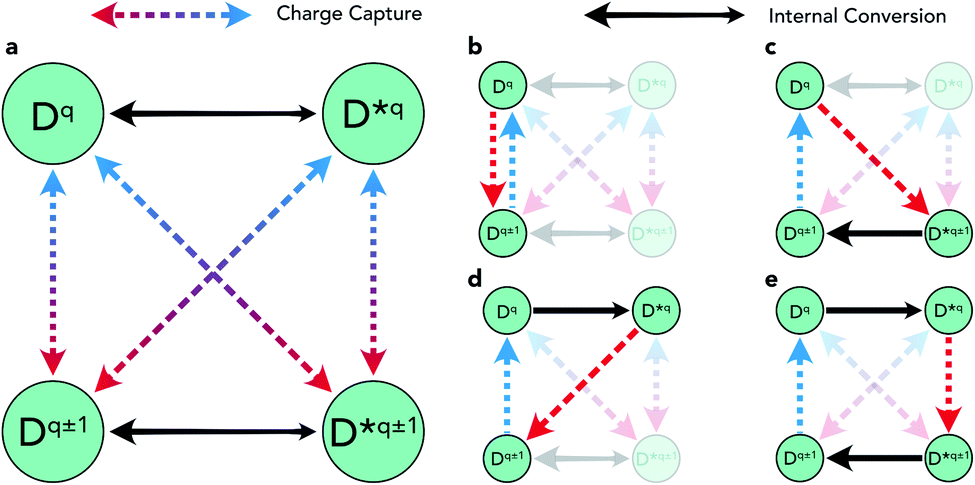 | ||
| Fig. 1 (a) Graph network illustration of the potential structural transitions involving charge capture (red/blue) or internal conversion (black) for a defect D in charge state q. A single metastable configuration D*q is assumed to be accessible for each charge state. (b) Pathway for a typical 2-step Shockley–Read–Hall recombination process. (c) Pathway for a 3-step recombination process involving capture into a metastable defect structure, followed by internal relaxation and charge capture back to the initial state. (d) Pathway for a 3-step recombination process involving internal excitation to a metastable structure, followed by electron and hole charge capture. (e) Pathway for a 4-step recombination process involving internal excitation to a metastable structure (D*q), charge capture to the q ± 1 metastable structure (D*q±1), internal relaxation and charge capture back to the initial configuration (Dq) | ||
The impact of these metastable defects depends on the competing charge capture rates (dashed red/blue arrows), the relative energies of and transition barriers between ground and metastable configurations (i.e. their accessibility) (solid black arrows) and the defect energy level position in the host band gap (eqn (1)). Each of the charge capture transitions can be fast or slow, with no necessary correlation between opposing directions. That said, the recurrence of harmonic PESs means that often a fast electron capture rate implies slow hole capture in the reverse direction, and vice versa.1,9,19 This is typically the result of the defect level lying close to the valence or conduction band, often yielding strong/weak interaction with the near/distant band edge and thus fast/slow carrier capture. This is the intuitive rationale behind the expectation that deep midgap defect levels will act as efficient recombination centres.1,16,19,20 In many cases however, this trend is violated as a result of anharmonicity in the defect PES, often arising due to symmetry-breaking in the defect structure.7,9,21 The prevalence of this phenomenon in semiconductors is becoming increasingly better understood, owing to advances in experimental characterisation and computational modelling techniques.1,9,11,22–24 On the other hand, there is a clear and definite correlation between the opposing internal conversion directions, indicated by the relative sizing of the black arrows in Fig. 1. The transition energy barrier from ground to higher energy metastable configuration must be larger than the reverse, hence kD→D* < kD*→D where k is the transition rate constant (i.e. it is always easier to thermally relax than to excite).
Transitions to higher charge states (q ± 2) have not been included here as the behaviour is mostly equivalent and, regardless, for recombination to occur, a closed path must be established (as in Fig. 1b–e), returning the defect to the initial configuration. That said, two ways in which q ± 2 defects could influence the overall recombination rate here is (1) by introducing rapid capture into, but slow capture out of, these extremal charge states, thus acting to inhibit recombination as defects get ‘stuck’ in inert charge states,1,16,21 or (2) the rare scenario where Dq±2 introduces an alternative low-barrier pathway between Dq±1 and D*q±1 which does not exist otherwise, potentially accelerating the recombination process (i.e. introducing an additional path along the lower rim of the graph network in Fig. 1a).
Fig. 1c serves as an illustrative example of the potential acceleration or deceleration of the recombination cycle by metastable structures, with the rate of the internal relaxation (black arrow) from D*q±1 to Dq±1 being the deciding factor. Assuming rapid capture transitions for q → q* ± 1 (red) and q ± 1 → q (blue), a fast internal relaxation means that D*q±1 acts as a reaction intermediate, introducing a rapid pathway for the recombination cycle to proceed. If, however, internal conversion is extremely slow and D*q±1 does not readily relax to Dq±1, several alternative pathways may emerge. The long-lived metastable configuration could undergo charge capture and return back to the original Dq, completing the e–h recombination cycle without involving Dq±1. Such behaviour would increase/decrease the overall recombination rate if the rate-limiting step for Dq ⇔ D*q±1 was faster/slower than that of Dq ⇔ Dq±1. Instead, if the defect level is sufficiently close to a band edge D*q±1 could readily emit the captured charge, acting as a shallow defect level with no effect on the recombination rate. Alternatively, if D*q±1 has both slow internal relaxation and slow charge capture, defects could become ‘stuck’ in this inert state and in fact greatly diminish the overall recombination activity.
In the above discussion, only non-radiative (phonon emission) pathways are considered. Under certain conditions, both charge capture and internal conversion may also proceed radiatively through photon emission. A detailed consideration of such behaviour is beyond the scope of this report, though we note that it is non-radiative capture which dominates efficiency losses in PV semiconductors.1,4,25
Capture into metastable defects
In recent years, several papers have highlighted the decisive role that metastable defects can play in charge-carrier capture kinetics.9,16–18 In each of these studies, it is the situation described in Fig. 1c that is reported, where the defect Dq captures an electron or hole by transforming to a metastable configuration of the q ± 1 defect (D*q±1). This metastable species then relaxes to the ground-state Dq±1 through an internal conversion reaction, whether a spin-flip de-excitation16 or (more commonly) structural/vibrational relaxation,17,18 or both.9 In each case, this alternative pathway is found to proceed more rapidly than the standard Dq ⇔ Dq±1 charge capture process (Fig. 1b), thus enhancing the overall recombination rate and reconciling theoretical recombination models with experimental observations.The question of whether one should expect this to typically be the case, where the presence of a low-lying metastable structure D*q±1increases the recombination rate, is still up for discussion. The reporting of this phenomenon in the literature is undoubtedly biased, likely only to be discussed when the metastable defect accelerates recombination and ignored otherwise, thus discouraging any general conclusions based on the prevalence of these observations.
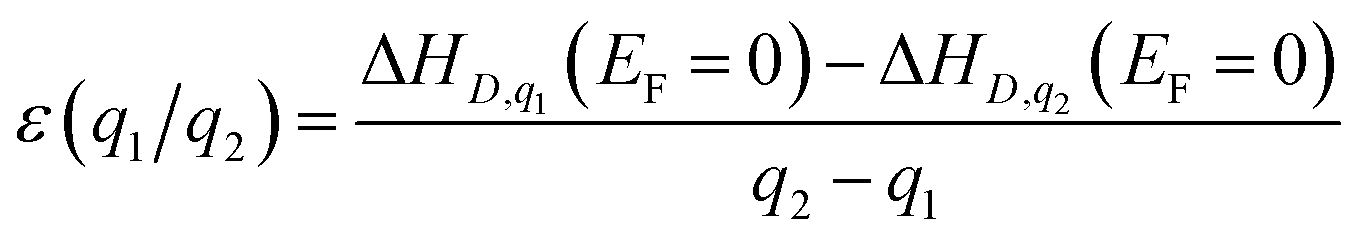
The shift in defect energy levels when metastable defects are involved (depicted in Fig. 2), does however permit some general expectations for the relative capture rates. As mentioned above, much of the electronic behaviour of point defects is dictated by the position of their energy levels in the semiconducting band gap. These in-gap levels are given by their ‘thermodynamic charge transition level’ (TL) positions ε(q1/q2), which are the Fermi level positions where the equilibrium charge state switches between q1 and q2, given by:
 | (1) |
| ΔHD*,q±1 = ΔHD,q±1 + ΔE | (2) |
| ε(q/q* ± 1) = ε(q/q ± 1) ∓ ΔE | (3) |
| e− capture ⇒ ε(q/q* − 1) = ε(q/q − 1) + ΔE | (4) |
| h+ capture ⇒ ε(q/q* + 1) = ε(q/q + 1) − ΔE | (5) |
 | ||
| Fig. 2 Charge transition level positions for ground-state ε(q/q ± 1) and ground-state ⇔ metastable configurations ε(q/q* ± 1), on a defect formation energy diagram (left) and a vertical energy level diagram (right). | ||
Thus we witness that for charge capture into a metastable structure, Dq → D*q±1, the transition level will move an energy ΔE closer to the corresponding band edge (i.e. to higher energy in the band gap for electron capture or to lower energy for hole capture), assuming a transition level ε(q/q ± 1) initially located within the band gap. Conversely, this shift in TL position also means the TL will be located further from the relevant band edge for the D*q±1 → Dq transition (capture from the metastable defect). For example, the ε(0/−1*) transition level is located closer to the CBM, from which electrons are captured by D0 to form D*−1, than ε(0/−1), but further from the VBM, from which D*−1 could capture holes to complete the recombination cycle. Under the conventional rationale of capture rates being exponentially dependent on the separation of the defect level from the band edge,1,9,19,20 this implies a faster capture into the metastable configuration (Dq → D*q±1) than the ground-state process (Dq → Dq±1), but a slower capture rate in the opposite direction (D*q±1 → Dq). As discussed above, if D*q±1 can swiftly relax to Dq±1, the situation depicted in Fig. 1c emerges. Here the ‘best of both’ is obtained, with electron capture proceeding via the TL nearest the conduction band and hole capture via the TL nearest the valence band, likely expediting the recombination process as observed in ref. 9 and 16–18. Crucially, the introduction of the internal conversion to the recombination kinetics means that the timescale of the D*q±1 → Dq±1 transition, relative to the slowest charge capture process, will dictate whether the metastable defect accelerates or retards the overall recombination rate. Given typical effective vibrational (attempt) frequencies of ∼0.5–10 THz,9,18,26 internal conversion is unlikely to be the rate-limiting step in a fast recombination cycle if the transition energy barrier ΔE is less than 0.2–0.4 eV (Section S3.1†).
Another important consideration is that for the metastable configuration to enter the recombination process, the transition level ε(q/q* ± 1) must lie within the band gap formed between the valence band maximum (VBM) and conduction band minimum (CBM):
| EVBM < ε(q/q* ± 1) < ECBM | (6) |
| EVBM < ε(q/q ± 1) ∓ ΔE < ECBM | (7) |
| ε(q/q − 1) + ΔE < ECBM | (8) |
| e− capture ⇒ ΔE < ECBM − ε(q/q − 1) | (9) |
| EVBM < ε(q/q + 1) − ΔE | (10) |
| h+ capture ⇒ ΔE < ε(q/q + 1) − EVBM | (11) |
As an example, in CdTe, there are 6 intrinsic defects (two vacancies, antisites and interstitials each), which range in charge from 0 to either −2 or +2 for a Fermi level within the band gap (except TeCd which ranges from −2 to +2).27 These 20 defect species yield 14 in-gap levels involving only ground-state structures. With our recently-published defect structure-searching technique (see Methods),11,12 we further identify 14 metastable structures for these charge states, generating 32 additional charge transition levels. Only 12 of these structures are sufficiently low energy to yield at least one transition level within the band gap, including those for Tei discussed here and VCd discussed in ref. 9, yielding 18 transition levels involving metastable structures in the CdTe band gap. Of course, the presence of low-energy metastable defect structures in a given material will depend on several factors, including the bulk crystal symmetry, chemical bonding, and band gap, amongst others.
We note that Fig. 2 also serves as an illustrative example of the fluctuations in charge transition level positions that temperature and strong electron–phonon coupling would engender, yielding a distribution of energy levels rather than a static trap. Such behaviour could then influence the non-radiative recombination process in a similar fashion to the impact of metastability discussed here, with non-linear temperature dependence in capture cross-sections—an important consideration when interpreting the results of spectroscopic defect measurements.28
Capture from metastable defects
As illustrated by Fig. 1d and e, metastable configurations can also enter the recombination cycle through an initial thermal or optical excitation, prior to charge capture. Again, the metastable defect D*q could have a slower or faster capture rate than the corresponding ground-state configuration Dq. In the case of faster capture (kD*→Dq±1 > kD→Dq±1), the metastable configuration acts as an accelerating reaction intermediate to electron–hole recombination through the path Dq → D*q → Dq±1 → Dq (Fig. 1d). This mechanism is similar to the Dq → D*q±1 → Dq±1 → Dq route (Fig. 1c) discussed in the previous section, though with some crucial differences in the governing kinetics (now involving an internal excitation, rather than relaxation). If accessible metastable configurations exist for both charge states, then recombination could also proceed through the pathway shown in Fig. 1e, with the charge capture transition occurring between the metastable defects D*q → D*q±1, prior to de-excitation and charge capture back to Dq. While certainly possible, to our knowledge a defect centre exhibiting this behaviour has not been previously reported in the literature, which may be attributed to the recency of advancements in atomistic modelling of non-radiative carrier recombination4–6,8,29 and our understanding of the importance of metastable structures in these processes.9,16–18 Interestingly, we note that an analogous hot-electron capture mechanism was however invoked to explain the puzzling experimental observations of charge capture behaviour for negative-U DX centres in AlxGa1−xAs in the 1980s.30 | ||
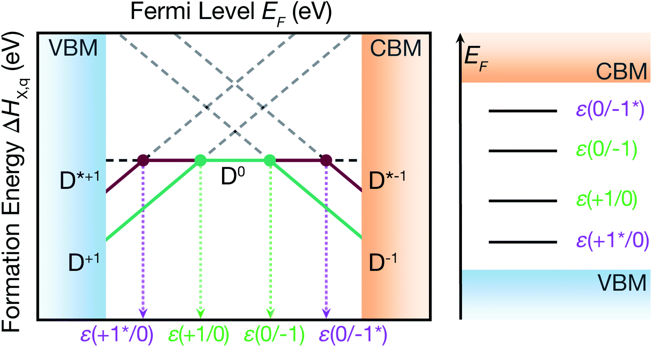
Fig. 3 Atomic structures of ground-state (Te0/+1i) and metastable  tellurium interstitials in CdTe, looking down the [001] axis. Atoms sized according to their formal ionic radii.31 Te anions are shown in gold and Cd cations in purple. tellurium interstitials in CdTe, looking down the [001] axis. Atoms sized according to their formal ionic radii.31 Te anions are shown in gold and Cd cations in purple. | ||
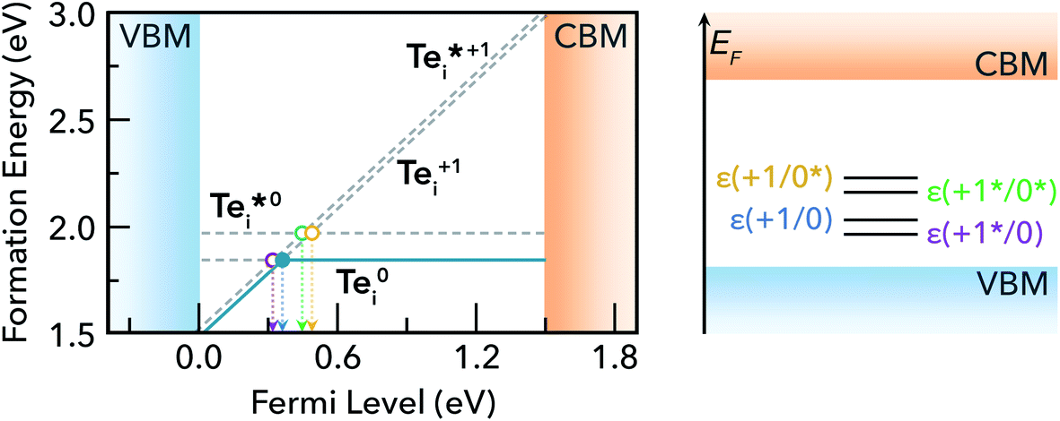 | ||
| Fig. 4 (Left) Defect formation energy diagram for the neutral and positively charged states of Tei in CdTe, under Te-rich conditions (μTe = 0). The equilibrium charge state is shown in solid blue, and higher energy states in dashed grey. (Right) Vertical energy band diagram showing the Tei (+(*)/0(*)) charge transition levels in CdTe. | ||
We find that Tei has two low-energy structural arrangements for both the neutral and positively charged interstitial, resulting in four potential charge transitions (i.e. intersection points on the transition level diagram in Fig. 4). In both the neutral and positively-charged ground-states, the interstitial Tei displaces a host Te atom to form a split-interstitial Te–Te dimer (Fig. 3), as first noted by Du et al.32 For Te+1i, the dimer bond is directed along the 〈110〉 crystal direction, adopting a C2v point group symmetry. For Te0i, the dimer bond is twisted slightly (12°) about the [001] axis, thus reducing to C2 point group symmetry with the removal of the {110} mirror plane.
A standard ab initio geometry relaxation from the high-symmetry tetrahedral interstitial coordination does not find the neutral ground-state Te0i, but rather converges to a higher-energy structure  with a formation energy only 127 meV higher than the split-interstitial dimer ground-state (Fig. 4). This configuration exhibits two short (2.90 Å) and two long (3.86 Å) Tei–Te distances, and an apical Tei–Cd bond (2.66 Å) yielding C2v point symmetry (Fig. 3). In fact, this structure is a saddle point on the PES, representing the transition state of the Tei interstitial diffusion mechanism (i.e. hopping of the split-interstitial dimer).26,33,34 We thus determine a diffusion barrier of 0.13 eV for Te0i using the HSE(34.5%) + SOC functional (Fig. S2†), similar to the literature value of 0.09 eV calculated using both GGA (PBE) and hybrid (HSE06) DFT.26,33 A similar metastable structure exists for the positively-charged interstitial
  , where the partial occupancy of the defect level induces a Jahn–Teller splitting of the two long Tei–Te bonds, thus reducing to Cs point symmetry (Fig. 3). Here, the metastable configuration
  is only 36 meV higher in energy than the ground-state Te+1i, now exhibiting a local stability window of 40 meV (Fig. S2†).
 , the C2v structure involves two Te neighbours moving closer to the interstitial atom, and two moving away (Fig. 3), giving a configurational degeneracy of
 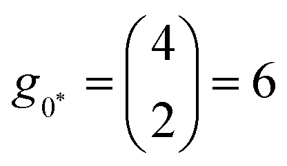 . The splitting of the two long Te–Te bonds in the Cs
 structure (Fig. 3) further doubles the number of equivalent structural configurations, yielding g+1* = 24 when also accounting for the spin degeneracy factor.
The consequences of degeneracy mismatches between ground and metastable defect structures can be exemplified by the temperature-dependent ‘reduced energy’ Er:35–37
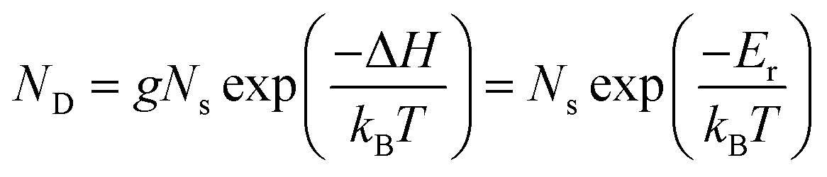 | (12) |
Er = ΔH − kBT![[thin space (1/6-em)]](https://www.rsc.org/images/entities/char_2009.gif) ln(g) ln(g) | (13) |
 at room temperature, while for Te0i the greater degeneracy of the ground-state disfavours the metastable configuration. Notably, such entropic effects become even more significant at elevated temperatures (for example during crystal growth and annealing where defects are initially introduced—strongly affecting the resulting self-consistent Fermi level) and for cases with larger degeneracy differences (potentially over an order of magnitude). This phenomenon is another important consequence of symmetry-breaking and metastable configurations for point defects in semiconductors, which can significantly impact bulk defect concentrations and thus Fermi level position, in addition to the effects on non-radiative recombination discussed here.
 in CdTe
| Defect | Point symmetry | g site | g spin | g total | ΔH (meV) | E r(T = 300 K) (meV) |
|---|---|---|---|---|---|---|
| Te0i | C 2 | 12 | 1 | 12 | 0 | 0 |

|
C 2v | 6 | 1 | 6 | 127 | 145 |
| Te+1i | C 2v | 6 | 2 | 12 | 0 | 0 |

|
C s | 12 | 2 | 24 | 36 | 18 |
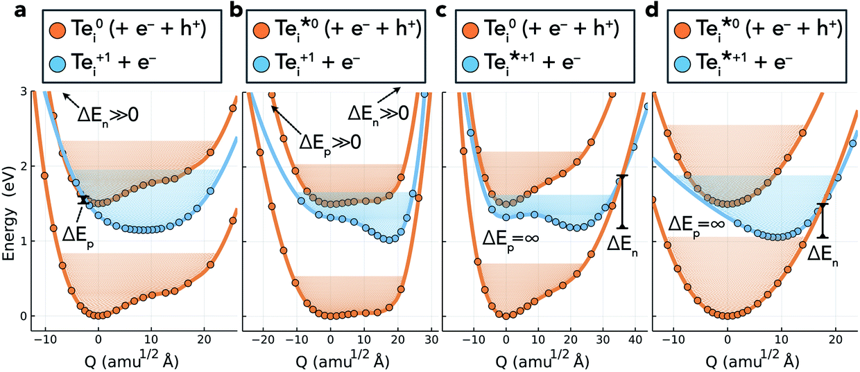 | ||
| Fig. 5 Potential energy surfaces (PESs) corresponding to the four Tei (+(*)/0(*)) charge transition levels in CdTe. Filled circles denote datapoints calculated with hybrid DFT including spin–orbit coupling, and the solid lines are spline interpolations. The low-lying effective vibrational states are shown by the shaded regions, and ΔEn/p represents the classical energy barrier to the capture transition. Q is the 1D structural coordinate along the path between equilibrium configurations, given in units of mass-weighted displacement. Transitions from the upper orange to blue PESs (Te0i → Te+1i) correspond to hole capture, while those from blue to lower orange correspond to electron capture (Te+1i → Te0i) | ||
By calculating the electron–phonon coupling (Wif = 〈Ψi|∂Ĥ/∂Q|Ψf〉) and solving the 1D Schrödinger equation to determine the effective vibrational wavefunctions for the calculated energy surfaces, the non-radiative recombination activity of the corresponding defect transition levels (TLs) may be computed, with the results for Tei provided in Table 2 and Fig. 6. The relationship between the calculated PESs and resultant capture rates can be intuitively understood through the classical energy barriers to charge capture, denoted by ΔEn/p in Fig. 5. A small capture barrier ΔEn/p and/or close overlap of the defect PESs near the equilibrium position typically yields fast carrier capture, while large barriers and/or significant separation of PESs results in slow capture rates.
| TL (wrt. VBM) (eV) | ΔQ (amu1/2 Å) | Carrier | ΔE (eV) | g capture | W if (eV amu−1/2 Å−1) | C n/p (300 K) (cm3 s−1) | σ n/p (300 K) (cm2) |
|---|---|---|---|---|---|---|---|
| a The charge capture path degeneracy is the number of equivalent paths on the PES from the initial to final state, entering as a multiplicative factor in the capture rate. | |||||||
| (+/0) @ 0.35 eV | 8.47 | e− | >4 | 2 | 2.40 × 10⁻² | 3.30 × 10⁻¹⁸ | 8.70 × 10⁻²⁶ |
| h+ | 0.08 | 2 | 1.70 × 10⁻² | 2.30 × 10⁻⁸ | 1.00 × 10⁻¹⁵ | ||
| (+/0*) @ 0.48 eV | 17.43 | e− | 2.23 | 12 | 2.40 × 10⁻³ | 4.10 × 10⁻¹⁹ | 1.10 × 10⁻²⁶ |
| h+ | 3.43 | 8 | 1.30 × 10⁻³ | 8.60 × 10⁻¹⁰ | 4.00 × 10⁻¹⁷ | ||
| (+*/0) @ 0.32 eV | 21.94 | e− | 0.72 | 8 | 2.90 × 10⁻³ | 1.50 × 10⁻¹¹ | 4.10 × 10⁻¹⁹ |
| h+ | ∞ | 2 | 5.70 × 10⁻³ | 2.30 × 10⁻⁹ | 1.10 × 10⁻¹⁶ | ||
| (+*/0*) @ 0.44 eV | 9.27 | e− | 0.43 | 1 | 2.10 × 10⁻³ | 1.20 × 10⁻¹¹ | 3.20 × 10⁻¹⁹ |
| h+ | ∞ | 4 | 2.30 × 10⁻² | 1.10 × 10⁻⁷ | 5.20 × 10⁻¹⁵ | ||
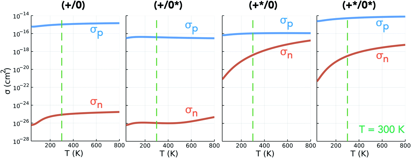 | ||
| Fig. 6 Electron and hole capture cross-section (σn and σp) as functions of temperature T for the Tei (+(*)/0(*)) charge transition levels in CdTe. Room temperature (T = 300 K) denoted by the dashed green line as a guide for typical solar cell operating conditions. | ||
Inspecting the defect PESs in Fig. 5 and corresponding capture rates in Table 2 & Fig. 6, we firstly note that all four potential transition pathways exhibit fast hole capture: 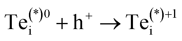 , with close overlap of the PESs about the upper orange
 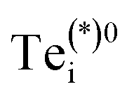 minimum in each case. This behaviour is consistent with the conventional rationale of fast hole capture for defect levels located near the VBM, as is the case here (Fig. 4). The large hole capture cross-sections σp ∼ 10−15 cm2 – of similar magnitude to its atomic cross-section σTe = π(aTe)2 ≃ 1.5 × 10⁻¹⁵ cm2 – classify Tei as a ‘giant’ hole trap.25,38,39 On the other hand, we witness negligible electron capture due to high barriers and low PES overlap for the (+/0) and (+/0*) transition levels (Fig. 5a and b), with tiny capture cross-sections σn ∼ 10−26 cm2. It is only when
 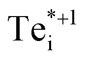 is involved, as in the (+*/0) and (+*/0*) levels in Fig. 5c and d, that a tractable electron capture barrier ΔEn emerges, yielding an increase in the electron capture rate by over 6 orders of magnitude to σn ∼ 10−19 cm2 (Table 2 and Fig. 6). To contextualise, we note that ‘giant’ traps or ‘killer’ defects are typically classified as those with capture cross-sections σ ∼ 10−15 to 10−13 cm2, for moderate traps σ ∼ 10−20 to 10−15 cm2 and weak traps σ < 10−20 cm2.4,25,39 Of course, the overall rate of capture (R) remains dependent on the defect and carrier concentrations (ND and n) in the material (R ∝ NDσn), meaning defects with moderate capture cross-sections can act as performance-limiting species if they form easily in the bulk, as is the case for Tei in commercial Te-rich CdTe.
The slow electron capture rates of the (+/0) and (+/0*) TLs rule out the possibility of significant Shockley–Read–Hall e–h recombination through the typical two-step process (Fig. 1b), or indeed through the recently reported capture–relaxation–capture process discussed previously (Fig. 1c). The large σn of  does, however, permit electron–hole recombination to proceed through the three-step and four-step process shown in Fig. 1d and e, involving internal excitation from the ground-state of the positive interstitial
 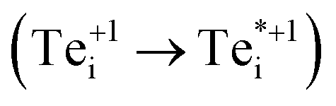 , before electron capture to either the ground-state or metastable neutral interstitial
 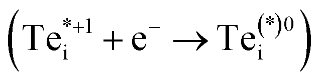 , and finally fast hole capture to complete the recombination cycle. For the thermal excitation
  , we calculate an energy barrier of 0.08 eV (Fig. S2†) and an effective vibrational attempt frequency ν = 0.40 THz, yielding a room temperature transition rate k+/+* = 7.6 × 10¹⁰ s−1, using transition state theory. This internal conversion occurs far more rapidly than the rate-limiting electron capture process (
 n ≃ (1.5 × 10⁻¹¹ cm3 s−1)(1012 cm−3) ≃ 101 s−1), as is also the case for the barrier-less
  vibrational relaxation. Further details for these calculations are provided in Section S3.†
We observe facile thermal transformation between Tei defect structures under typical solar cell operating conditions (black arrows in Fig. 1d, e and 7), with electron capture by  representing the rate-limiting step in the recombination kinetics—now proceeding >6 orders of magnitude faster than for the ground-state Te+1i. In summary, without the presence of the metastable
  , tellurium interstitials would behave as benign defect centres, only capable of capturing holes and later emitting them, reducing carrier mobilities but having no effect on recombination. However, by introducing alternative pathways for electron capture to proceed, the low-lying metastable +1 structure facilitates the 3-step and 4-step recombination cycles shown in Fig. 1d, e and 7, transforming Tei into an important recombination centre in Te-rich CdTe.
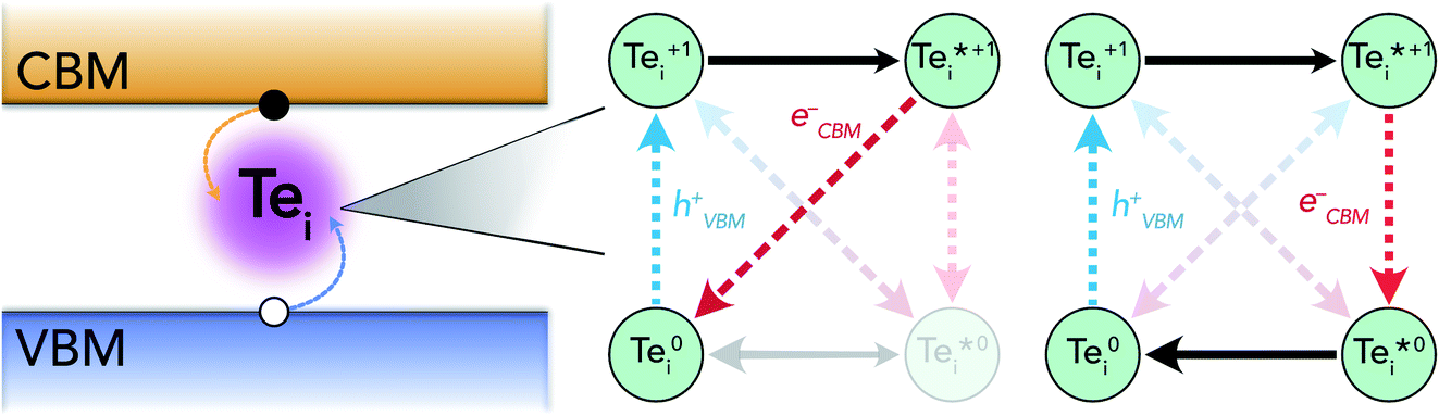 | ||
| Fig. 7 Schematic of the proposed non-radiative recombination mechanism at tellurium interstitials in CdTe. Red/blue arrows denote electron/hole capture, and black arrows indicate internal conversion reactions. | ||
Accordingly, these findings yield important considerations. Semiconductors exhibiting strong anharmonicity and mixed ionic–covalent bonding (e.g. Bi, Sb and Sn-based materials),1,41 low crystal symmetry (e.g. Sb2X3)42,43 and/or compositional complexity (e.g. multinary compounds such as CZTS and double perovskites)44–46 are likely to manifest local minima on defect energy surfaces. Low-energy metastable defect structures may be especially prevalent in emerging inorganic PV materials which tend to exhibit these properties, highlighting the potential importance of these species to investigations of non-radiative recombination and open-circuit voltage deficits in emerging solar cells. Indeed, even in the case of the high-symmetry binary semiconductor CdTe, many low energy metastable structures exist, introducing 18 additional charge transition levels in the gap and accelerating the carrier trapping at Tei and VCd.9 An important factor in the emergence of the thermal-excitation capture pathway here is the high mobility of the Te interstitial in CdTe, as demonstrated by the low diffusion barriers calculated in this and previous works.26,33,34 The facile ionic diffusion of Tei is a simultaneous consequence of the soft, anharmonic PESs which cause the ready accessibility of distinct structural motifs (i.e. low-lying metastable structures), facilitating this complex recombination pathway. Thus, we additionally propose rapid diffusion as a potential indicator of this behaviour at other semiconductor defect centres. Finally, we note that the very presence of metastable structures on the defect PES implies a softer and more anharmonic energy landscape, with smaller barriers between structures. As exemplified in this and other studies,7,9,21,47 such effects often yield unintuitive recombination kinetics, with fast trapping despite deep energy levels.
In conclusion, metastable defect structures impact non-radiative recombination in semiconductors. They introduce a complex set of potential recombination paths at defects, akin to chemical reaction mechanisms, with the overall kinetics being a function of the individual transition rates. In addition to the thermal-relaxation pathway discussed in recent works,9,16–18 we demonstrate that metastable defect structures can also enter the recombination cycle via thermal excitation, provided the internal transformation energy barrier is sufficiently small. We focus on the tellurium interstitial (Tei) in CdTe solar cells as an illustrative example of this phenomenon, exhibiting complex 3-step and 4-step recombination cycles which, to our knowledge, have not been previously reported in the literature. In addition to demonstrating the major potential impact of metastable structures on defect-mediated electron–hole recombination, Tei serves a clear example of anharmonicity causing deviation from the typical trend of reduced capture rates with deeper defect levels (i.e. greater energy separation from the band edge). Finally, we highlight implications to the broader field of photovoltaic materials research. We pose that metastable defect structures are more important to non-radiative recombination than currently understood, particularly in the case of emerging inorganic PV materials which often exhibit reduced crystal symmetries, mixed ionic–covalent bonding, multinary compositions and/or highly-mobile defects like Tei, where anharmonicity, symmetry-breaking and soft potential energy surfaces are likely to yield many low-lying, easily-accessible metastable structures, enabling the behaviour discussed here.
Methods
Anharmonic carrier capture coefficients were calculated using CarrierCapture.jl,5 with electron–phonon coupling matrix elements determined using the method outlined in ref. 6. In-depth details of the computational implementation are provided in ref. 9. All of the underlying total energy calculations were performed using Density Functional Theory (DFT) within periodic boundary conditions through the Vienna Ab Initio Simulation Package (VASP), employing Projector-Augmented Wave (PAW) pseudopotentials.48–51 The screened hybrid DFT exchange–correlation functional of Heyd, Scuseria and Ernzerhof (HSE),52 including spin–orbit interactions (SOC), was used for all calculations. An exact Hartree–Fock exchange fraction of αexx = 34.5% was employed in the hybrid DFT model, reproducing the room temperature experimental band gap of 1.5 eV for CdTe. A 64-atom, 13.1 Å cubic supercell was used for defect calculations, with a well-converged 450 eV plane-wave energy cutoff, a 2 × 2 × 2 Γ-centred Monkhorst–Pack k-point mesh and a force convergence criterion of 0.01 eV Å−1 for geometry optimization. The ShakeNBreak defect structure-searching method which aids the efficient location of ground and metastable structures for defects in solids was employed.11,12Data availability
Data produced during this work is freely available at https://doi.org/10.5281/zenodo.5999057.Conflicts of interest
There are no conflicts to declare.Acknowledgements
Seán R. Kavanagh acknowledges the EPSRC Centre for Doctoral Training in the Advanced Characterisation of Materials (CDT-ACM) (EP/S023259/1) for funding a PhD studentship, as well as the Max-Planck-Institut für Eisenforschung and the Thomas Young Centre for funding a research visit through the ‘Coffee with Max Planck’ and Junior Research Fellowship awards. DOS acknowledges support from the EPSRC (EP/N01572X/1) and from the European Research Council, ERC (Grant No. 758345). AW acknowledges support from a National Research Foundation of Korea (NRF) grant funded by the Korean Government (MSIT) (2018R1C1B6008728). We acknowledge the use of the UCL Kathleen High Performance Computing Facility (Kathleen@UCL), the Imperial College Research Computing Service, and associated support services, in the completion of this work. Via membership of the UK’s HEC Materials Chemistry Consortium, which is funded by the EPSRC (EP/L000202, EP/R029431, EP/T022213), this work used the ARCHER2 UK National Supercomputing Service (https://www.archer2.ac.uk) and the UK Materials and Molecular Modelling (MMM) Hub (Thomas – EP/P020194 & Young – EP/T022213).References
- Y.-T. Huang, S. R. Kavanagh, D. O. Scanlon, A. Walsh and R. L. Z. Hoye, Nanotechnology, 2021, 32, 132004 CrossRef CAS PubMed.
- U. Rau, B. Blank, T. C. M. Müller and T. Kirchartz, Phys. Rev. Appl., 2017, 7, 044016 CrossRef.
- H. Jin, E. Debroye, M. Keshavarz, I. G. Scheblykin, M. B. J. Roeffaers, J. Hofkens and J. A. Steele, Mater. Horiz., 2020, 7, 397–410 RSC.
- A. Alkauskas, Q. Yan and C. G. Van de Walle, Phys. Rev. B: Condens. Matter Mater. Phys., 2014, 90, 075202 CrossRef CAS.
- S. Kim, S. N. Hood, P. van Gerwen, L. D. Whalley and A. Walsh, CarrierCapture.Jl: Anharmonic Carrier Capture, Zenodo, 2020, DOI:10.5281/zenodo.3707592.
- M. E. Turiansky, A. Alkauskas, M. Engel, G. Kresse, D. Wickramaratne, J.-X. Shen, C. E. Dreyer and C. G. Van de Walle, Comput. Phys. Commun., 2021, 267, 108056 CrossRef CAS.
- S. Kim, S. N. Hood and A. Walsh, Phys. Rev. B, 2019, 100, 041202 CrossRef CAS.
- L. Shi and L.-W. Wang, Phys. Rev. Lett., 2012, 109, 245501 CrossRef PubMed.
- S. R. Kavanagh, A. Walsh and D. O. Scanlon, ACS Energy Lett., 2021, 6, 1392–1398 CrossRef CAS PubMed.
- A. Zakutayev, J. D. Major, X. Hao, A. Walsh, J. Tang, T. K. Todorov, L. H. Wong and E. Saucedo, J. Phys.: Energy, 2021, 3, 032003 CAS.
- I. Mosquera-Lois and S. R. Kavanagh, Matter, 2021, 4, 2602–2605 CrossRef.
- I. Mosquera-Lois, S. R. Kavanagh, A. Walsh and D. O. Scanlon, arXiv, 2022, preprint, arXiv:2207.09862 [cond-mat].
- C. J. Krajewska, S. R. Kavanagh, L. Zhang, D. J. Kubicki, K. Dey, K. Gałkowski, C. P. Grey, S. D. Stranks, A. Walsh, D. O. Scanlon and R. G. Palgrave, Chem. Sci., 2021, 12, 14686–14699 RSC.
- W. Goes, Y. Wimmer, A. M. El-Sayed, G. Rzepa, M. Jech, A. L. Shluger and T. Grasser, Microelectron. Reliab., 2018, 87, 286–320 CrossRef CAS.
- S. Lany and A. Zunger, Phys. Rev. Lett., 2004, 93, 156404 CrossRef PubMed.
- A. Alkauskas, C. E. Dreyer, J. L. Lyons and C. G. Van de Walle, Phys. Rev. B, 2016, 93, 201304 CrossRef.
- D. Guo, C. Qiu, K. Yang and H.-X. Deng, Phys. Rev. Appl., 2021, 15, 064025 CrossRef CAS.
- J.-H. Yang, L. Shi, L.-W. Wang and S.-H. Wei, Sci. Rep., 2016, 6, 21712 CrossRef CAS PubMed.
- B. Das, I. Aguilera, U. Rau and T. Kirchartz, Phys. Rev. Mater., 2020, 4, 024602 CrossRef CAS.
- T. Kirchartz, T. Markvart, U. Rau and D. A. Egger, J. Phys. Chem. Lett., 2018, 9, 939–946 CrossRef CAS PubMed.
- X. Zhang, M. E. Turiansky and C. G. Van de Walle, J. Phys. Chem. C, 2020, 124, 6022–6027 CrossRef CAS.
- E. Menéndez-Proupin and W. Orellana, Phys. Status Solidi B, 2015, 252, 2649–2656 CrossRef.
- A. Shepidchenko, B. Sanyal, M. Klintenberg and S. Mirbt, Sci. Rep., 2015, 5, 1–6 Search PubMed.
- Y. Kumagai, N. Tsunoda, A. Takahashi and F. Oba, Phys. Rev. Mater., 2021, 5, 123803 CrossRef CAS.
- A. M. Stoneham, Theory of Defects in Solids: Electronic Structure of Defects in Insulators and Semiconductors, Oxford University Press, 2001 Search PubMed.
- J.-H. Yang, J.-S. Park, J. Kang and S.-H. Wei, Phys. Rev. B: Condens. Matter Mater. Phys., 2015, 91, 075202 CrossRef.
- J.-H. Yang, W.-J. Yin, J.-S. Park, J. Ma and S.-H. Wei, Semicond. Sci. Technol., 2016, 31, 083002 CrossRef.
- D. Wickramaratne, C. E. Dreyer, B. Monserrat, J.-X. Shen, J. L. Lyons, A. Alkauskas and C. G. Van de Walle, Appl. Phys. Lett., 2018, 113, 192106 CrossRef.
- L. Shi, K. Xu and L.-W. Wang, Phys. Rev. B: Condens. Matter Mater. Phys., 2015, 91, 205315 CrossRef.
- T. N. Theis and P. M. Mooney, MRS Online Proc. Libr., 1989, 163, 729–740 CrossRef.
- R. D. Shannon, Acta Crystallogr., Sect. A: Cryst. Phys., Diffr., Theor. Gen. Crystallogr., 1976, 32, 751–767 CrossRef.
- M.-H. Du, H. Takenaka and D. J. Singh, J. Appl. Phys., 2008, 104, 093521 CrossRef.
- J. Ma, J. Yang, S.-H. Wei and J. L. F. Da Silva, Phys. Rev. B: Condens. Matter Mater. Phys., 2014, 90, 155208 CrossRef.
- S. C. Selvaraj, S. Gupta, D. Caliste and P. Pochet, Appl. Phys. Lett., 2021, 119, 062105 CrossRef CAS.
- R. Grau-Crespo, S. Hamad, C. R. A. Catlow and N. H. de Leeuw, J. Phys.: Condens. Matter, 2007, 19, 256201 CrossRef.
- P. T. Landsberg, Recombination in Semiconductors, 1992 Search PubMed.
- W. Hayes and A. M. Stoneham, Defects and Defect Processes in Nonmetallic Solids, Wiley, New York, 1985 Search PubMed.
- L. Pauling, The Nature of the Chemical Bond and the Structure of Molecules and Crystals: An Introduction to Modern Structural Chemistry, Cornell University Press, Ithaca New York, 3rd edn, 1961 Search PubMed.
- S. Kim, J. A. Márquez, T. Unold and A. Walsh, Energy Environ. Sci., 2020, 13, 1481–1491 RSC.
- W. Shockley and W. T. Read, Phys. Rev., 1952, 87, 835–842 CrossRef CAS.
- S. R. Kavanagh, C. N. Savory, D. O. Scanlon and A. Walsh, Mater. Horiz., 2021, 8, 2709–2716 RSC.
- X. Wang, Z. Li, S. R. Kavanagh, A. M. Ganose and A. Walsh, Phys. Chem. Chem. Phys., 2022, 24, 7195–7202 RSC.
- M. Huang, Z. Cai, S. Wang, X.-G. Gong, S.-H. Wei and S. Chen, Small, 2021, 17, 2102429 CrossRef CAS PubMed.
- J. Li, Z.-K. Yuan, S. Chen, X.-G. Gong and S.-H. Wei, Chem. Mater., 2019, 31, 826–833 CrossRef CAS.
- Z. Li, S. R. Kavanagh, M. Napari, R. G. Palgrave, M. Abdi-Jalebi, Z. Andaji-Garmaroudi, D. W. Davies, M. Laitinen, J. Julin, M. A. Isaacs, R. H. Friend, D. O. Scanlon, A. Walsh and R. L. Z. Hoye, J. Mater. Chem. A, 2020, 8, 21780–21788 RSC.
- S. Kim, J.-S. Park, S. N. Hood and A. Walsh, J. Mater. Chem. A, 2019, 7, 2686–2693 RSC.
- X. Zhang, M. E. Turiansky, J.-X. Shen and C. G. Van de Walle, Phys. Rev. B, 2020, 101, 140101 CrossRef CAS.
- G. Kresse and J. Hafner, Phys. Rev. B: Condens. Matter Mater. Phys., 1993, 47, 558–561 CrossRef CAS PubMed.
- G. Kresse and J. Hafner, Phys. Rev. B: Condens. Matter Mater. Phys., 1994, 49, 14251–14269 CrossRef CAS PubMed.
- G. Kresse and J. Furthmüller, Comput. Mater. Sci., 1996, 6, 15–50 CrossRef CAS.
- P. E. Blöchl, Phys. Rev. B: Condens. Matter Mater. Phys., 1994, 50, 17953–17979 CrossRef PubMed.
- J. Heyd, G. E. Scuseria and M. Ernzerhof, J. Chem. Phys., 2003, 118, 8207–8215 CrossRef CAS.
Footnote |
| † Electronic supplementary information (ESI) available. See https://doi.org/10.1039/d2fd00043a |
| This journal is © The Royal Society of Chemistry 2022 |