
Ultrahigh carrier mobility contributes to remarkably enhanced thermoelectric performance in n-type PbSe†
Yu
Xiao
 *a,
Liqing
Xu
a,
Tao
Hong
b,
Haonan
Shi
b,
Sining
Wang
b,
Xiang
Gao
c,
Xiangdong
Ding
a,
Jun
Sun
a and
Li-Dong
Zhao
*b
*a,
Liqing
Xu
a,
Tao
Hong
b,
Haonan
Shi
b,
Sining
Wang
b,
Xiang
Gao
c,
Xiangdong
Ding
a,
Jun
Sun
a and
Li-Dong
Zhao
*b
aState Key Laboratory for Mechanical Behavior of Materials, Xi'an Jiaotong University, Xi'an 710049, China. E-mail: xiao_yu@xjtu.edu.cn
bSchool of Materials Science and Engineering, Beihang University, Beijing 100191, China. E-mail: zhaolidong@buaa.edu.cn
cCenter for High Pressure Science and Technology Advanced Research (HPSTAR), Beijing 100094, China
First published on 25th November 2021
Abstract
A high average ZT value (ZTave) of ∼1.13 in an n-type PbSe-based thermoelectric material at 300–873 K has been achieved in this work. Its high thermoelectric performance originates from ultrahigh carrier mobility in the whole working temperature range through synergistically tuning the carrier effective mass, carrier density and microstructure. To maximize the carrier mobility in n-type PbSe, the conduction band shape is firstly optimized through SnS alloying to lower the carrier effective mass, which can benefit a high carrier mobility. Moreover, the carrier density is reoptimized to match its lowered carrier effective mass with Cu interstitial doping, and the suppressed carrier–carrier scattering can further enhance its carrier mobility, leading to a maximum carrier mobility of ∼6081 cm2 V−1 S−1 and a maximum power factor of ∼26.1 μW cm−1 K−2 at 300 K in PbSe–18%SnS–0.5%Cu. Additionally, the microstructure observation reveals that the intrinsically layered SnS phase can be endotaxially embedded as cubic SnS nanocrystals to form semi-coherent phase boundaries in a PbSe matrix, which also plays a significant role in maintaining carrier transmission and simultaneously blocking phonons. With these well optimized carrier and phonon transport properties, the room-temperature ZT value reaches ∼0.6 and continuously increases to ∼1.6 at 773 K in n-type PbSe–18%SnS–0.5%Cu. This remarkably enhanced thermoelectric performance in this work outperforms that of previously reported n-type PbSe-based materials.
Broader contextA thermoelectric material is capable of realizing direct and reversible heat-to-electricity conversion. A high thermoelectric conversion efficiency requires optimization of the carrier and phonon transports in the material. To date, strategies for band engineering and nanostructuring have been well developed to tune carrier effective mass and suppress phonon transport properties, respectively. However, methods to optimize the carrier mobility are neglected in previous studies. Herein, we attempt to systematically investigate the carrier mobility in n-type PbSe-based thermoelectric materials with the following successive steps. Firstly, the carrier effective mass in n-type PbSe is reduced by band sharpening, which can contribute to high carrier mobility. Secondly, Cu interstitial doping in PbSe–18%SnS can suppress the carrier density at low temperature and dynamically optimize the carrier density at high temperature, which can largely enhance the carrier mobility because of reduced carrier scattering. Thirdly, the semi-coherent grain boundary formed in the matrix not only suppresses the phonon transport properties but also maintains a high carrier mobility. As a result, the well optimized carrier mobility contributes to a high ZTave of ∼1.13 in PbSe–18%SnS–0.5%Cu at 300–873 K. This result highlights the importance of optimizing carrier density in thermoelectric materials, and these strategies could be effectively extended to other materials. |
Introduction
Thermoelectric materials are capable of directly converting waste heat into electricity, which can improve the utilization efficiency of fossil energy and has attracted much attention from the energy community.1–3 The conversion efficiency of a thermoelectric device depends on the dimensionless figure of merit, ZT = S2σT/κtot, where S, σ, T, and κtot denote the Seebeck coefficient, electrical conductivity, absolute temperature in kelvin and total thermal conductivity, respectively. Distinctly, an ideal thermoelectric material should simultaneously possess a large Seebeck coefficient, high electrical conductivity and low total thermal conductivity. However, these intricated interrelations between thermoelectric parameters make it challengeable to achieve a high ZT value.4–6To date, most developed strategies for improving the thermoelectric performance are to balance these thermoelectric parameters and aim at obtaining an enhancement of the net ZT value,7–13 including band structure manipulations to enhance electrical transport properties14–16 and defect structure design to reduce thermal conductivity.17–21 Notably, these strategies above will inevitably deteriorate the carrier mobility, which is closely related to the Seebeck coefficient and electrical conductivity, thus limiting the final improvement of the thermoelectric performance. Recently, researchers have become increasingly aware of the importance of maintaining carrier mobility in high-performance thermoelectric materials,22–25 especially in compounds featured with a single electronic band structure, such as n-type lead chalcogenides.26–28
In thermoelectric materials, carrier mobility might be affected by multiple factors, such as the deformation potential, carrier effective mass, carrier density and defects in the matrix.29,30 Specifically, the deformation potential describes the carrier scattering strength by acoustic phonons, and it is often difficult to regulate on a large scale from previous results.31,32 Carrier effective mass is another important parameter and has a reciprocal relationship with carrier mobility, namely, a large carrier effective mass theoretically exhibits relatively low carrier mobility and vice versa. Carrier density usually can be flexibly regulated through doping and also presents an inversely proportional relationship with carrier mobility, because higher carrier density will cause stronger carrier–carrier scattering to reduce carrier mobility. Defect designing is a common method of reducing lattice thermal conductivity in thermoelectric materials by intensifying phonon scattering, but it could concurrently strengthen scattering to carrier. Therefore, to maximize the carrier mobility in thermoelectric materials, it is necessary to rationally optimize these important factors discussed above. Recently, many methods have been explored and well developed to tune carrier mobility, including band sharpening,33–35 light doping or dynamic doping,36–40 sub-nanostructure designing,41,42etc.
This work takes the n-type PbSe as an example and illustrates the strategies for maximizing its carrier mobility and thermoelectric performance. Firstly, the carrier effective mass in n-type PbSe is optimized by SnS alloying, and the room-temperature carrier effective mass decreases from ∼0.34 me in Pb0.99Sb0.01Se to ∼0.25 me in Pb0.99Sb0.01Se–30%SnS, which benefits a maximum carrier mobility of ∼303 cm2 V−1 s−1 in SnS-alloyed PbSe. To match the reduced carrier effective mass in SnS-alloyed PbSe, the carrier density is further reoptimized with Cu atoms as an interstitial dopant. The obtained optimal carrier density is ∼8.9 × 1017 cm−3 at 300 K and such a low carrier density results in an ultrahigh carrier mobility of ∼6081 cm2 V−1 s−1 in n-type PbSe–18%SnS–0.5%Cu sample. More importantly, Cu interstitials in n-type PbSe–18%SnS–0.5%Cu presents a dynamic doping behavior, thus making the carrier density continuously increase from ∼8.9 × 1017 cm−3 at 300 K to ∼9.9 × 1018 cm−3 at 773 K. This special dynamic doping behavior can effectively optimize the carrier mobility in the whole temperature range and avoid bipolar diffusion at the high temperature range.40 Additionally, the microstructure observation in PbSe–18%SnS–0.5%Cu reveals that SnS-based nanostructures form semi-coherent phase boundaries in the PbSe matrix, which is favorable for maintaining high carrier mobility and simultaneously blocking phonon transmission. With these successive strategies for optimizing carrier mobility, a room-temperature ZT value ∼0.6 and a maximum ZT value ∼1.6 at 773 K have been realized in n-type PbSe–18%SnS–0.5%Cu.
Results and discussion
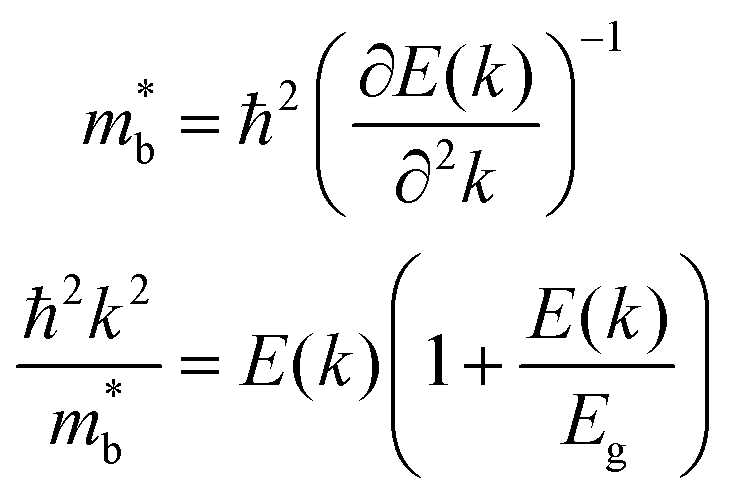
To enhance the thermoelectric performance in n-type PbSe, this work focuses on optimizing its carrier mobility. Firstly, based on the Sb-doped n-type PbSe, SnS alloying in PbSe is conducted to lower its carrier effective mass due to band sharpening, and this lowered carrier effective mass can theoretically benefit high carrier mobility. Secondly, to match the reduced carrier effective mass in SnS-alloyed PbSe, the carrier density is reoptimized with Cu interstitial doping in PbSe–18%SnS–x%Cu (x = 0.2–1.0), largely enhancing its carrier mobility and power factor in the whole temperature range. Finally, microstructure observation reveals that SnS can crystalize in a cubic structure with a nanoscale size and form a semi-coherent phase boundary in the PbSe lattice, which is favorable for maintaining high carrier mobility and simultaneously reducing lattice thermal conductivity.Using these successive methods, an ultrahigh carrier mobility of ∼6081 cm2 V−1 S−1 at 300 K can be achieved in PbSe–18%SnS–0.5%Cu, as shown in Fig. 1(a). In the relationship between carrier density and carrier mobility, PbSe–18%SnS–x%Cu (x = 0.2–1.0) samples own the highest carrier mobility compared with other high-performance n-type PbSe-based thermoelectric materials, such as high-entropy PbSe,43 PbSe (AgSbSe2),44 PbSe (Cd),45 PbSe (Ge),46 PbSe (Cu/Te),47 PbSe (Cr),48 PbSe (Cu),36 PbSe (Pb).49 Additionally, among these n-type PbSe-based thermoelectric materials, PbSe–18%SnS–x%Cu (x = 0.2–1.0) samples not only maintain high carrier mobility but also achieve relatively low lattice thermal conductivity due to the induced nanostructures by SnS alloying and Cu doping, as shown in Fig. 1(b). As a result, the final ZT value in PbSe–18%SnS–x%Cu (x = 0.2–1.0) samples undergoes a large enhancement in the whole working temperature range. A room-temperature ZT value of ∼0.6 and a maximum ZT value of ∼1.6 at 773 K have been realized in PbSe–18%SnS–0.5%Cu, which results in a high average ZTave value of ∼1.13 at 300–873 K, shown in Fig. 1(c). Such a high average ZTave value makes the PbSe–18%SnS–0.5%Cu sample outstanding among previously reported n-type PbSe-based thermoelectric materials at 300–873 K, including ∼0.96 in high-entropy PbSe,43 ∼0.84 in PbSe (AgSbSe2),44 ∼0.97 in PbSe (Ge),46 ∼1.02 in PbSe (Cu/Te),47 ∼1.0 in PbSe (Cu)36 and ∼0.78 in PbSe (Cr)48 shown in Fig. 1(d).
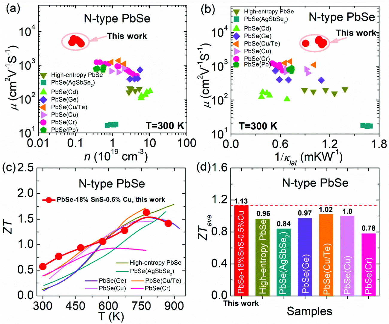 | ||
| Fig. 1 (a) Comparison of carrier mobility as a function of carrier density in n-type PbSe; (b) comparison of carrier mobility as a function of 1/κlat in n-type PbSe; (c) comparison of temperature-dependent ZT value in n-type PbSe; (d) comparison of ZTave value in n-type PbSe-based thermoelectric materials at 300–873 K. | ||
Crystal structure identification and bandgap evolution in Pb0.99Sb0.01Se–x%SnS (x = 0–30).
The powder X-ray diffraction (XRD) patterns of Pb0.99Sb0.01Se–x%SnS (x = 0–30) are shown in Fig. 2(a). As SnS content increases, the peak shift to high angle is clearly observed in Pb0.99Sb0.01Se–x%SnS (x = 0–30) because of the lattice shrinking in PbSe after SnS alloying, which is consistent with the evaluated lattice parameters in Fig. 2(b). Notably, extra SnS peaks can be found when SnS alloying content is above 24%. Therefore, the lattice parameter linearly decreases with increasing SnS content and then remains invariable when the solid solubility of SnS reaches solid solution limitation. Correspondingly, the measured optical bandgap of Pb0.99Sb0.01Se–x%SnS (x = 0–30) samples also undergoes a similarly decreasing tendency with the increase of SnS content, as shown in Fig. 2(c). Specifically, the room temperature optical bandgap gradually decreases from ∼0.30 eV in Pb0.99Sb0.01Se to ∼0.15 eV in Pb0.99Sb0.01Se–24%SnS. Notably, the bandgap in Pb0.99Sb0.01Se–x%SnS (x = 0–30) approaches its limitation when SnS content is above ∼24% and the bandgap in Pb0.99Sb0.01Se–30%SnS sample cannot be clearly fitted due to its low absorption coefficient at high photon energy (0.3–0.5 eV), which could be caused by an amount of the SnS phase with a large bandgap (Eg ∼1.16 eV) in the PbSe matrix, as revealed by the XRD results in Fig. 2(a). Obviously, the measured bandgap in Fig. 2(d) is consistent with the variations of lattice parameter in Pb0.99Sb0.01Se–x%SnS (x = 0–30), proving a high solid solubility of SnS in the PbSe matrix. | ||
| Fig. 2 Phase identification and bandgap measurement in Pb0.99Sb0.01Se–x%SnS (x = 0–30): (a) XRD patterns; (b) lattice parameter as a function of SnS content; (c) room-temperature optical spectrum of bandgap, and (d) fitted bandgap value as a function of SnS content. | ||
The band structure evolution in Pb0.99Sb0.01Se–x%SnS (x = 0–30) mainly arises from interaction of outer electrons between Sn and Pb atoms, and the higher Sn 5s electrons push the valence band into a higher energy level, causing a decrease of the bandgap at L point.50–52 The schematic image of band structure evolution in SnS-alloyed PbSe is presented in Fig. 3(a). With increasing SnS content in PbSe, the bandgap continuously decreases, accompanied by a process of band shape sharpening both in valence and conduction bands. In lead chalcogenides, the band shape and bandgap are inherently related to the carrier effective mass, and follows the relationships given below:53
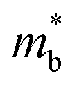 is single band effective mass, ℏ denotes the reduced Planck constant, E(k) is the electron dispersion relations, k denotes the wave vector, Eg is the bandgap. Therefore, a narrowed bandgap will cause a sharp band shape and lowered carrier effective mass, as shown in Fig. 3(b). With SnS alloying in n-type PbSe, the room-temperature bandgap and carrier effective mass decrease from ∼0.3 eV and ∼0.35 me in Pb0.99Sb0.01Se to ∼0.15 eV and ∼0.25 me in Pb0.99Sb0.01Se–30%SnS. And this reduced carrier effective mass (m*) can theoretically benefit a high carrier mobility (u) from the inversely proportional relationship u ∝ 1/m*, which favorably benefits a high thermoelectric performance in Pb0.99Sb0.01Se–x%SnS (x = 0–30).
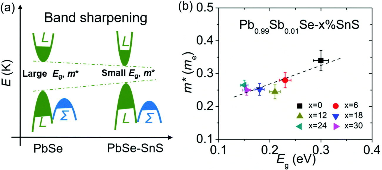 | ||
| Fig. 3 (a) Schematic image of band structure evolution and (b) room-temperature effective mass as a function of bandgap in Pb0.99Sb0.01Se–x%SnS (x = 0–30). | ||
Thermoelectric transport properties in Pb0.99Sb0.01Se–x%SnS (x = 0–30).
Fig. 4 shows the temperature-dependent thermoelectric properties in Pb0.99Sb0.01Se–x%SnS (x = 0–30). The electrical conductivity in Fig. 4(a) shows an obvious decreasing tendency with increasing SnS content, and the decreased electrical conductivity might mainly arise from intensified carrier scattering caused by SnS alloying and partly from reduced carrier density, as shown in Table S1 (ESI†). Correspondingly, the reduced carrier density in Pb0.99Sb0.01Se–x%SnS (x = 0–30) is consistent with the enhanced absolute value of the Seebeck coefficient in Fig. 4(b). The Pisarenko relationship in Fig. S1 (ESI†) indicates that SnS alloying in n-type PbSe can reduce the carrier effective mass due to band sharpening discussed above. With triple effects on carrier transport properties in Pb0.99Sb0.01Se–x%SnS (x = 0–30), including reduced carrier effective mass, lowered carrier density and defects induced by SnS alloying, the measured room-temperature carrier mobility finally undergoes first increasing and then decreasing tendency with increasing SnS content, and the maximum carrier mobility can be achieved at ∼303 cm2 V−1 S−1 in Pb0.99Sb0.01Se–12%SnS, as shown in Fig. S2 (ESI†). Consequently, the enhanced carrier mobility in Pb0.99Sb0.01Se–x%SnS (x = 0–30) can maintain a high power factor and the maximum power factor increases from ∼16.9 μW cm−1 K−2 at 773 K in Pb0.99Sb0.01Se to ∼19.3 μW cm−1 K−2 at 673 K in Pb0.99Sb0.01Se–18%SnS, as shown in Fig. 4(c).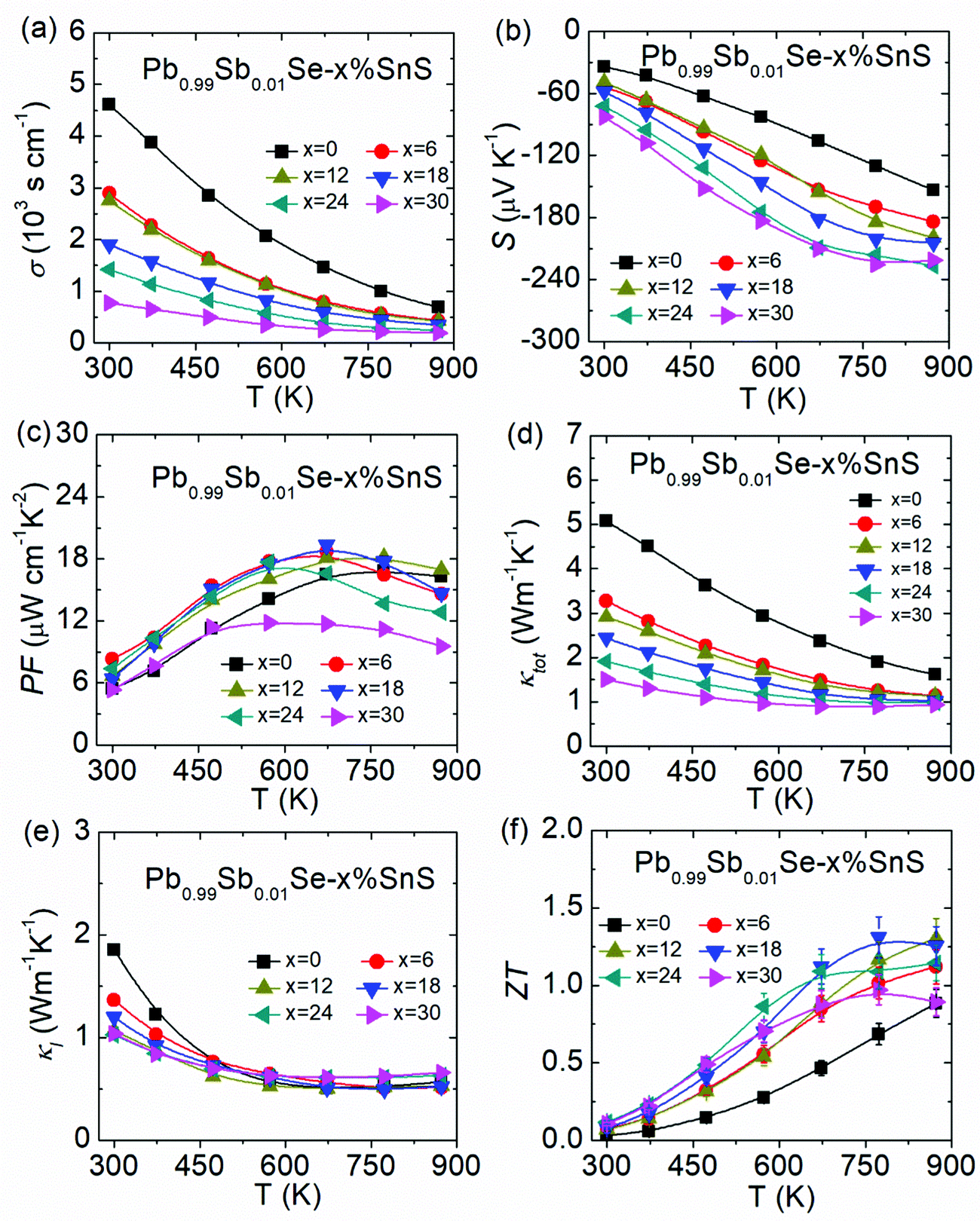 | ||
| Fig. 4 Temperature-dependent thermoelectric transport properties in Pb0.99Sb0.01Se–x%SnS (x = 0–30): (a) electrical conductivity; (b) Seebeck coefficient; (c) power factor; (d) total thermal conductivity; (e) lattice thermal conductivity; (f) ZT values. | ||
Fig. 4(d) presents the temperature-dependent total thermal conductivity in Pb0.99Sb0.01Se–x%SnS (x = 0–30). Obviously, the total thermal conductivity is largely reduced after SnS alloying, and the room-temperature total thermal conductivity decrease from ∼5.08 W m−1 K−1 in Pb0.99Sb0.01Se to ∼1.50 W m−1 K−1 in Pb0.99Sb0.01Se–30%SnS, which results from both reduced electronic thermal conductivity and lattice thermal conductivity, as shown in Fig. S3(d) (ESI†) and Fig. 4(e), respectively. The origin of reduced lattice thermal conductivity will be discussed in the following microstructure observation part and more detailed thermal transport properties can be found in Fig. S3 (ESI†). As a result, the final ZT value in SnS-alloyed Pb0.99Sb0.01Se is obviously enhanced in the whole working temperature range, and the maximum ZT value is improved from ∼0.9 in Pb0.99Sb0.01Se to ∼1.3 in Pb0.99Sb0.01Se–18%SnS, as shown in Fig. 4(f).
Electrical transport properties in PbSe–18%SnS–x%Cu (x = 0.2–1.0) with reoptimized carrier density.
Among the thermoelectric parameters, carrier effective mass and carrier density share a proportional relationship, and rationally optimizing these two critical parameters is important to enhance electrical transport properties.35,54 To match the lowered carrier effective mass in Pb0.99Sb0.01Se–18% SnS, Cu interstitial doping is chosen to replace Sb doping in PbSe–18%SnS–x%Cu (x = 0.2–1.0), because Cu interstitial can be more effectively optimize electrical transport properties at low carrier density, which has been widely applied and proved in lead chalcogenides.36,37,41,55,56 As shown in Fig. S4 (ESI†), extra Cu doping in PbSe–18%SnS maintains a cubic phase, and the lattice parameter increases with increasing Cu doping content, which indicates that Cu atoms can enter into the interstitial sites and cause lattice expansion in the PbSe matrix. It is worth pointing out that Cu interstitial doping in PbSe–18%SnS–x%Cu (x = 0.2–1.0) causes insignificant effects on the electronic band structure and the room-temperature bandgap remains around ∼0.15 eV, as shown in Fig. S5 (ESI†).In fact, the undoped PbSe–18%SnS sample shows p-type transport properties around the room temperature range and undergoes a p–n transition with increasing temperature, as depicted in Fig. S6 (ESI†). The Hall measurement results in Fig. 5(a) present that Cu doping in PbSe–18%SnS–x%Cu (x = 0.2–1.0) can effectively convert the p-type PbSe–18%SnS into electron-dominated n-type transport behavior in PbSe–18%SnS–x%Cu (x = 0.2–1.0). The reoptimized carrier density in PbSe–18%SnS–x%Cu (x = 0.2–1.0) varies within the range of ∼0.8–1.4 × 1018 cm−3 at 300 K. And the reduced carrier density in PbSe–18%SnS–x%Cu (x = 0.2–1.0) can well match its lowered carrier effective mass and result in largely enhanced carrier mobility, then a maximum carrier mobility of ∼6081 cm2 V−1 S−1 is achieved in PbSe–18%SnS–0.5%Cu. More importantly, different from static doping behavior in Sb-doped PbSe, high-temperature Hall measurements reveal that Cu interstitial doping in PbSe–18%SnS–0.5%Cu shows a dynamic doping behavior with increasing temperature, and its carrier density continuously increases from ∼8.9 × 1017 cm−3 at 300 K to 0.99 × 1018 cm−3 at 773 K, as shown in Fig. 5(b). This special dynamically tuned carrier density in PbSe–18%SnS–x%Cu (x = 0.2–1.0) can greatly optimize carrier mobility in the whole working temperature range, making PbSe–18%SnS–0.5%Cu maintain an exceptionally high carrier mobility, from ∼6081 cm2 V−1 S−1 at 300 K to ∼201 cm2 V−1 S−1 at 773 K in Fig. 5(c). With the reoptimized carrier density and largely enhanced carrier mobility, the PbSe–18%SnS–x%Cu (x = 0.2–1.0) samples present a relatively high electrical conductivity and Seebeck coefficient, shown in Fig. 5(d) and (e). Finally, the power factor in PbSe–18%SnS–x%Cu (x = 0.2–1.0) is remarkably enhanced, and the maximum power factor (PFmax) and average power factor (PFave) increases from PFmax ∼19.3 μW cm−1 K−2 and PFave ∼15.3 μW cm−1 K−2 in Pb0.99Sb0.01Se–18%SnS to PFmax ∼26.1 μW cm−1 K−2 and PFave ∼19.5 μW cm−1 K−2 in PbSe–18%SnS–0.5%Cu at 300–873 K, as shown in Fig. 5(f) and Fig. S7 (ESI†), respectively. Compared with other n-type PbSe-based thermoelectric materials, PbSe–18%SnS–0.5%Cu presents a competitive power factor especially at high temperature range, as shown in Fig. S8 (ESI†).
 | ||
| Fig. 5 Electrical transport properties in PbSe–18%SnS–x%Cu (x = 0.2–1.0): (a) room-temperature carrier density and carrier mobility as a function of Cu doping content; temperature-dependent (b) carrier density; (c) carrier mobility; (d) electrical conductivity; (e) Seebeck coefficient; and (f) power factor. | ||
Microstructure observation in PbSe–18%SnS–0.5%Cu
To investigate the structural origins of the optimized thermoelectric transport properties in PbSe–18%SnS–0.5%Cu, scanning transmission electron microscopy (STEM) is employed to see the detailed structural features. The medium-magnification STEM image in Fig. 6(a) presents a high density of precipitates with the width and length in dozens of nanometers. The nanoprecipitates can be seen more clearly in the higher magnification image in Fig. S9(a) (ESI†). The high-resolution transmission electron microscopy (HRTEM) image in the inset of Fig. 6(a) also shows a precipitate. The electron diffraction patterns shown in Fig. 6(b1) and Fig. 6(b2) are obtained in different selected regions, the PbSe matrix along the [100] and nanoprecipitate-included part. Interestingly, the electron diffraction pattern of the precipitate region shows a superposition, and the weak spots can be indexed into a cubic SnS phase that is considered to be endotaxially precipitated out along cubic PbSe grain boundary. Such an endotaxial relation between SnS nanocrystals and PbSe matrix can be clearly reflected in the enlarged HRTEM image in Fig. 6(c). It is obviously seen that the cubic SnS nanocrystal has an interplanar spacing of ∼3.25 Å along [1–11], and the SnS nanocrystals form a semi-coherent phase interface with the PbSe matrix. Besides, the semi-coherent phase boundary will also induce a strong strain field around the interfaces, as shown in the geometric phase analysis (GPA) in Fig. 6(d1 and d2). Therefore, this semi-coherent phase boundary in PbSe–18%SnS–0.5%Cu not only facilitates carrier transport but also strongly intensifies phonon scattering, which will be discussed in the thermal transport part. Fig. 6(e1–e5) present the STEM ADF image of SnS nanocrystals and the respective energy dispersion spectrum (EDS) mapping of Sn, S, Pb and Se. Notably, a slight deficiency of S element is shown in Fig. 6(e3) because S as the light element lacks sensitivity in EDS mapping compared with the Sn element and it is difficult to be distinguished from the Pb element due to their close characteristic peaks (Mα ∼2.341 KeV for Pb and Kα ∼2.309 KeV for S). The comparison of EDS results between the matrix and the nanoprecipitate is shown in Fig. 6(f), and EDS mapping of the Cu element in Fig. S9(c) (ESI†) proves a uniform distribution in PbSe–18%SnS–0.5%Cu.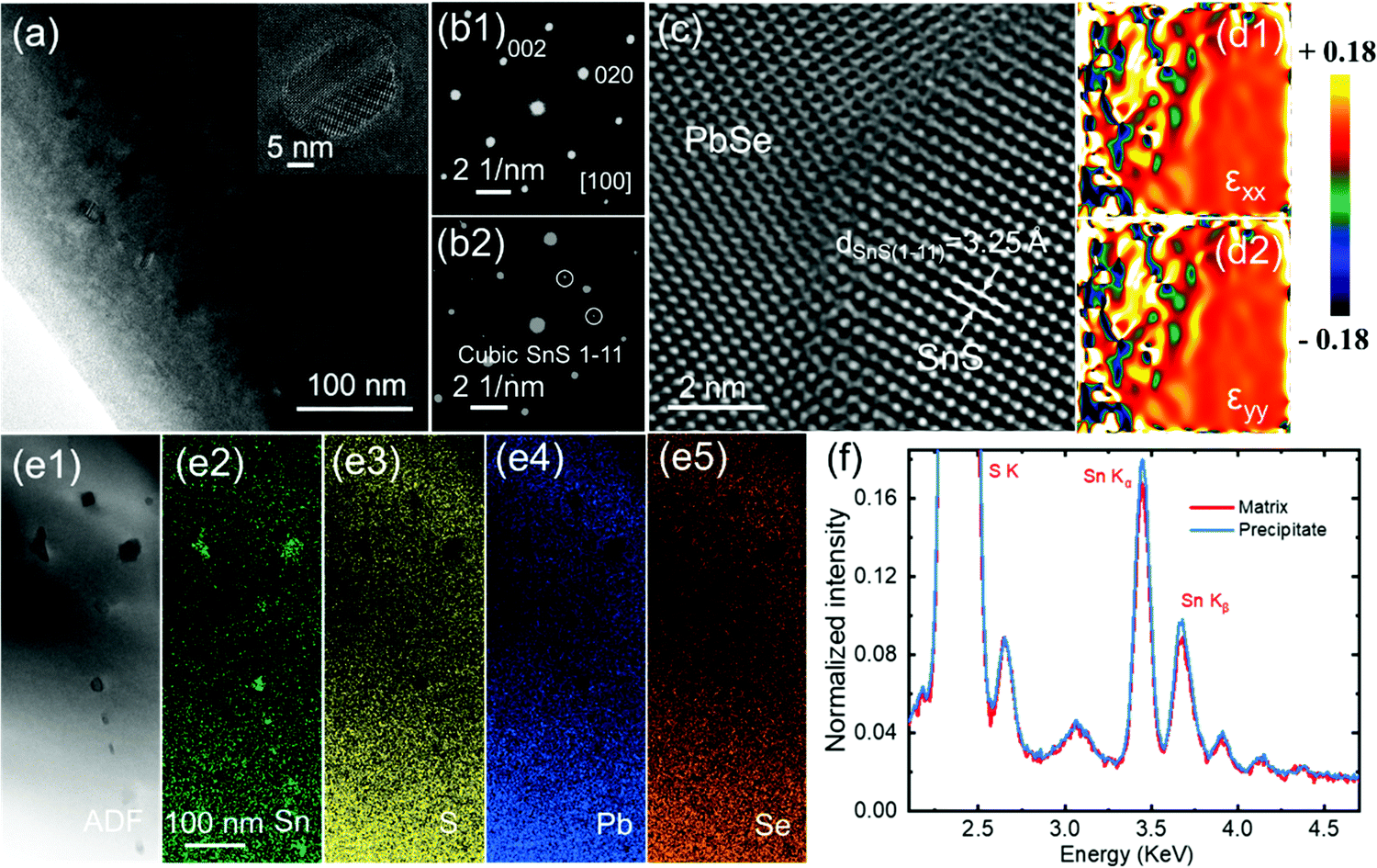 | ||
| Fig. 6 Microstructure observation in PbSe–18%SnS–0.5%Cu: (a) medium-magnification TEM image showing SnS precipitates in the PbSe matrix, the inset is the HRTEM image showing one SnS nano-precipitate; (b1–b2) electron diffraction pattern of the PbSe matrix along [100] and the diffraction spots of cubic SnS; (c) HRTEM image of the boundary between SnS precipitate and PbSe matrix; (d1–d2) strain maps (strain tensor εxx and εyy) reflect strong strain states around the precipitates and the distortion connection between precipitates; (e1–e5) STEM ADF image and the respective EDS mappings of Sn, S, Pb and Se; and (f) EDS results from matrix and precipitate, respectively. | ||
Thermal conductivity and the ZT value in PbSe–18%SnS–x%Cu (x = 0.2–1.0)
Besides the largely enhanced electrical transport properties, the thermal conductivity can also be distinctly reduced in PbSe–18%SnS–x%Cu (x = 0.2–1.0) with reoptimized carrier density and microstructure design. Fig. 7(a) shows that the total thermal conductivity is suppressed from ∼2.44 W m−1 K−1 in Pb0.99Sb0.01Se–18%SnS to ∼1.37 W m−1 K−1 in PbSe–18%SnS–0.5%Cu at 300 K. This low total thermal conductivity in PbSe–18%SnS–x%Cu (x = 0.2–1.0) arises from suppressed electronic thermal conductivity after reoptimizing carrier density and reduced lattice thermal conductivity due to intensified phonon scattering by nanostructures, as shown in Fig. S10(d) (ESI†) and Fig. 7(a), respectively. The minimum lattice thermal conductivity can achieve at ∼0.46 W m−1 K−1 in PbSe–18%SnS–1.0% at 873 K, which is close to its theoretical limitation of ∼0.37 W m−1 K−1 obtained by Cahill's model.57 More detailed thermal transport properties in PbSe–18%SnS–x%Cu (x = 0.2–1.0) can be found in Fig. S10(d) (ESI†). Combining the ultra-high carrier mobility and lowered lattice thermal conductivity, the final ZT value in PbSe–18%SnS–x%Cu (x = 0.2–1.0) is remarkably optimized in the whole temperature range in Fig. 7(b) (ESI†). Finally, a room-temperature ZT value of ∼0.6 and a maximum ZT value of ∼1.6 at 773 K in PbSe–18%SnS–0.5%Cu are obtained, which contributes to an exceptionally high average ZTave of ∼1.13 at 300–873 K. Remarkably, the cycle test results in Fig. S11 (ESI†) prove that PbSe–18%SnS–x%Cu (x = 0.2–1.0) samples have repeatable thermoelectric performance and high reliability.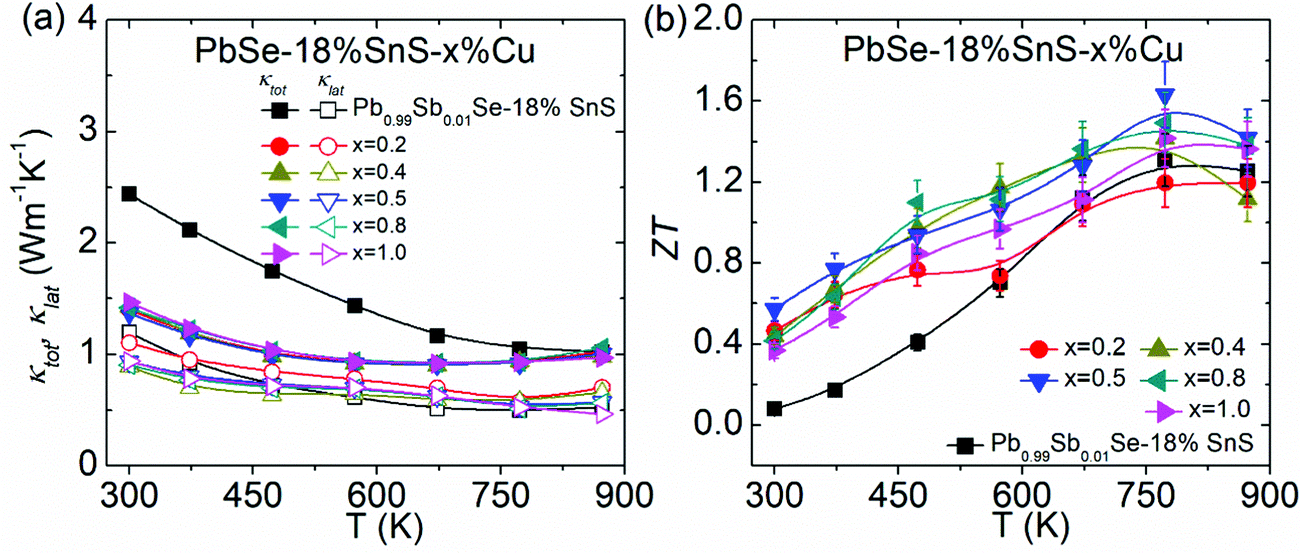 | ||
| Fig. 7 Temperature-dependent thermal conductivity and ZT value in PbSe–18%SnS–x%Cu (x = 0.2–1.0): (a) total thermal conductivity and lattice thermal conductivity; and (b) ZT value. | ||
Conclusions
A high-performance n-type PbSe–18%SnS–0.5%Cu sample with maximum ZT ∼1.6 at 773 K and ZTave ∼1.13 at 300–873 K has been achieved through full optimization of its carrier mobility. The obtained ultrahigh carrier mobility of ∼6081 cm2 V−1 S−1 in n-type PbSe–18%SnS–0.5%Cu stems from multiple effects: band sharpening caused by SnS alloying to tune its carrier effective mass; carrier density reoptimization through Cu interstitial doping to suppress the carrier–carrier scattering; semi-coherent phase boundary design through incorporating cubic SnS phase in the matrix to facilitate carrier transmission. With these rationally designed strategies, the electrical transport properties in n-type PbSe–18%SnS–0.5%Cu can be well optimized, and simultaneously its thermal conductivity is largely reduced due to strongly intensified phonon scattering caused by SnS alloying and Cu doping. Consequently, the considerably boosted power factor and reduced thermal conductivity can contribute to remarkably high thermoelectric performance in the n-type PbSe–18%SnS–0.5%Cu sample, making the performance in n-type PbSe comparable to its advanced p-type counterpart. More importantly, this work demonstrates the importance of carrier mobility optimization in high-performance thermoelectric materials, and these strategies used in this work could be also extended to other systems.Methods
All the highly densified PbSe samples in this work were prepared via the melting method and spark plasma sintering (SPS-211Lx) processes. The phase identification was checked by powder X-ray diffraction (PXRD) using Cu Kα radiation. The optical bandgap was measured using the infrared diffuse reflection method with a Fourier Transform Infrared Spectrometer (IRAffinity-1S). The Hall coefficient (RH) was measured using the van der Pauw method using a Lake Shore 8400 instrument. Scanning transmission electron microscopy (STEM) studies were conducted using a JEOL JEM-F200 electron microscope. Thermal diffusivity (D) was acquired on a Netzsch LFA457. The electrical conductivity and Seebeck coefficient were measured using a CTA instrument. The combined uncertainty for all measurements involved in the calculation of ZT was less than 20%. More experimental details can be found in the ESI.†Author contributions
The manuscript was written through contributions of all authors. All authors have given approval to the final version of the manuscript. Yu Xiao: conceptualization, data curation, writing-original draft, supervision, funding acquisition. Liqing Xu: data curation, writing-original draft, Tao Hong: TEM data curation; Haonan Shi: data curation, Sining Wang: data curation, Xiang Gao: TEM data curation; Xiangdong Ding: project administration, Jun Sun: project administration; Li-Dong Zhao: conceptualization, supervision, writing-review & editing, funding acquisition.Conflicts of interest
There are no conflicts to declare.Acknowledgements
We acknowledge the financial support from the Top Young Talents Programme of Xi’an Jiaotong University, the Fundamental Research Funds for the Central Universities, the National Natural Science Foundation of China (52172236 and 51772012), the National Key Research and Development Program of China (2018YFA0702100), the Beijing Natural Science Foundation (JQ18004) and the National Science Fund for Distinguished Young Scholars (51925101).References
- X.-L. Shi, J. Zou and Z.-G. Chen, Chem. Rev., 2020, 120, 7399–7515 CrossRef CAS.
- P. Sun, K. R. Kumar, M. Lyu, Z. Wang, J. Xiang and W. Zhang, Innovation, 2021, 2, 100101 Search PubMed.
- B. Qin, D. Wang, X. Liu, Y. Qin, J.-F. Dong, J. Luo, J.-W. Li, W. Liu, G. Tan, X. Tang, J.-F. Li, J. He and L.-D. Zhao, Science, 2021, 373, 556–561 CrossRef CAS.
- G. J. Snyder and E. S. Toberer, Nat. Mater., 2008, 7, 105–114 CrossRef CAS PubMed.
- J. Mao, G. Chen and Z. Ren, Nat. Mater., 2020, 20, 454–461 CrossRef.
- Y. Xiao and L.-D. Zhao, Science, 2020, 367, 1196–1197 CrossRef CAS.
- T. Zhu, Y. Liu, C. Fu, J. P. Heremans, J. G. Snyder and X. Zhao, Adv. Mater., 2017, 29, 1605884 CrossRef.
- G. Tan, L.-D. Zhao and M. G. Kanatzidis, Chem. Rev., 2016, 116, 12123–12149 CrossRef CAS.
- K. Zhao, P. Qiu, X. Shi and L. Chen, Adv. Funct. Mater., 2019, 30, 1903867 CrossRef.
- R. Nunna, P. Qiu, M. Yin, H. Chen, R. Hanus, Q. Song, T. Zhang, M.-Y. Chou, M. T. Agne and J. He, Energy Environ. Sci., 2017, 10, 1928–1935 RSC.
- D. Wu, Y. Pei, Z. Wang, H. Wu, L. Huang, L.-D. Zhao and J. He, Adv. Funct. Mater., 2014, 24, 7763–7771 CrossRef CAS.
- C. Chang, D. Y. Wang, D. S. He, W. K. He, F. Y. Zhu, G. T. Wang, J. Q. He and L. D. Zhao, Adv. Energy Mater., 2019, 9, 1901334 CrossRef.
- W. Zhao, Z. Liu, Z. Sun, Q. Zhang, P. Wei, X. Mu, H. Zhou, C. Li, S. Ma, D. He, P. Ji, W. Zhu, X. Nie, X. Su, X. Tang, B. Shen, X. Dong, J. Yang, Y. Liu and J. Shi, Nature, 2017, 549, 247–251 CrossRef CAS.
- Y. Pei, X. Shi, A. LaLonde, H. Wang, L. Chen and G. J. Snyder, Nature, 2011, 473, 66–69 CrossRef CAS.
- J. P. Heremans, V. Jovovic, E. S. Toberer, A. Saramat, K. Kurosaki, A. Charoenphakdee, S. Yamanaka and G. J. Snyder, Science, 2008, 321, 554–557 CrossRef CAS.
- M. Hong, Z.-G. Chen, L. Yang, Z.-M. Liao, Y.-C. Zou, Y.-H. Chen, S. Matsumura and J. Zou, Adv. Energy Mater., 2017, 8, 1702333 CrossRef.
- Y. He, P. Lu, X. Shi, F. F. Xu, T. S. Zhang, G. J. Snyder, C. Uher and L. D. Chen, Adv. Mater., 2015, 27, 3639–3644 CrossRef CAS.
- Z. H. Liu, W. H. Gao, X. F. Meng, X. B. Li, J. Mao, Y. M. Wang, J. Shuai, W. Cai, Z. F. Ren and J. H. Sui, Scr. Mater., 2017, 127, 72–75 CrossRef CAS.
- L. Yang, Z.-G. Chen, M. Hong, G. Han and J. Zou, ACS Appl. Mater. Interfaces, 2015, 7, 23694–23699 CrossRef CAS PubMed.
- B. Qin, D. Wang and L.-D. Zhao, InfoMat, 2021, 3, 755–789 CrossRef CAS.
- Y. Qiu, Y. Jin, D. Wang, M. Guan, W. He, S. Peng, R. Liu, X. Gao and L.-D. Zhao, J. Mater. Chem. A, 2019, 7, 26393–26401 RSC.
- C. Zhou, Y. K. Lee, Y. Yu, S. Byun, Z.-Z. Luo, H. Lee, B. Ge, Y.-L. Lee, X. Chen, J. Y. Lee, O. Cojocaru-Mirédin, H. Chang, J. Im, S.-P. Cho, M. Wuttig, V. P. Dravid, M. G. Kanatzidis and I. Chung, Nat. Mater., 2021, 20, 1378–1384 CrossRef CAS.
- A. Li, C. Hu, B. He, M. Yao, C. Fu, Y. Wang, X. Zhao, C. Felser and T. Zhu, Nat. Commun., 2021, 12, 5408 CrossRef CAS.
- G. J. Snyder, A. H. Snyder, M. Wood, R. Gurunathan, B. H. Snyder and C. Niu, Adv. Mater., 2020, 32, 2001537 CrossRef CAS.
- M. Samanta, K. Pal, U. V. Waghmare and K. Biswas, Angew. Chem., Int. Ed., 2020, 59, 4822–4829 CrossRef CAS.
- Y. Qin, Y. Xiao and L.-D. Zhao, APL Mater., 2020, 8, 010901 CrossRef CAS.
- Z. Hou, Y. Xiao and L.-D. Zhao, Nanoscale, 2020, 12, 12741–12747 RSC.
- Z.-Z. Luo, S. Hao, S. Cai, T. P. Bailey, G. Tan, Y. Luo, I. Spanopoulos, C. Uher, C. Wolverton and V. P. Dravid, J. Am. Chem. Soc., 2019, 141, 6403–6412 CrossRef CAS PubMed.
- L.-D. Zhao, S. Wang and Y. Xiao, Acta Metall. Sin., 2021, 57, 1171–1183 Search PubMed.
- J. Shuai, J. Mao, S. Song, Q. Zhu, J. Sun, Y. Wang, R. He, J. Zhou, G. Chen, D. J. Singh and Z. Ren, Energy Environ. Sci., 2017, 10, 799–807 RSC.
- H. Wang, Y. Pei, A. D. LaLonde and G. J. Snyder, Proc. Natl. Acad. Sci. U. S. A., 2012, 109, 9705–9709 CrossRef CAS PubMed.
- B. Zhu, X. Liu, Q. Wang, Y. Qiu, Z. Shu, Z. Guo, Y. Tong, J. Cui, M. Gu and J. He, Energy Environ. Sci., 2020, 13, 2106–2114 RSC.
- Y. Xiao, D. Wang, B. Qin, J. Wang, G. Wang and L.-D. Zhao, J. Am. Chem. Soc., 2018, 140, 13097–13102 CrossRef CAS PubMed.
- Y. Xiao, D. Wang, Y. Zhang, C. Chen, S. Zhang, K. Wang, G. Wang, S. J. Pennycook, G. J. Snyder, H. Wu and L.-D. Zhao, J. Am. Chem. Soc., 2020, 142, 4051–4060 CrossRef CAS PubMed.
- Y. Xiao, W. Liu, Y. Zhang, D. Wang, H. Shi, S. Wang, Y. Jin, W. Qu, H. Wu, X. Ding, J. Sun and L.-D. Zhao, J. Mater. Chem. A, 2021, 9, 23011–23018 RSC.
- L. You, Y. Liu, X. Li, P. Nan, B. Ge, Y. Jiang, P. Luo, S. Pan, Y. Pei, W. Zhang, G. J. Snyder, J. Yang, J. Zhang and J. Luo, Energy Environ. Sci., 2018, 11, 1848–1858 RSC.
- L. You, J. Zhang, S. Pan, Y. Jiang, K. Wang, J. Yang, Y. Pei, Q. Zhu, M. T. Agne, G. J. Snyder, Z. Ren, W. Zhang and J. Luo, Energy Environ. Sci., 2019, 12, 3089–3098 RSC.
- Q. Zhang, Q. Song, X. Wang, J. Sun, Q. Zhu, K. Dahal, X. Lin, F. Cao, J. Zhou and S. Chen, Energy Environ. Sci., 2018, 11, 933–940 RSC.
- X. Su, S. Hao, T. P. Bailey, S. Wang, I. Hadar, G. Tan, T. B. Song, Q. Zhang, C. Uher and C. Wolverton, Adv. Energy Mater., 2018, 8, 1800659 CrossRef.
- Y. Xiao, H. Wu, D. Wang, C. Niu, Y. Pei, Y. Zhang, I. Spanopoulos, I. T. Witting, X. Li, S. J. Pennycook, G. J. Snyder, M. G. Kanatzidis and L.-D. Zhao, Adv. Energy Mater., 2019, 9, 1900414 CrossRef.
- Y. Qin, T. Hong, B. Qin, D. Wang, W. He, X. Gao, Y. Xiao and L.-D. Zhao, Adv. Funct. Mater., 2021, 31, 2102185 CrossRef CAS.
- S. Wang, Y. Xiao, Y. Chen, S. Peng, D. Wang, T. Hong, Z. Yang, Y. Sun, X. Gao and L.-D. Zhao, Energy Environ. Sci., 2021, 14, 451–461 RSC.
- B. Jiang, Y. Yu, J. Cui, X. Liu, L. Xie, J. Liao, Q. Zhang, Y. Huang, S. Ning, B. Jia, B. Zhu, S. Bai, L. Chen, S. J. Pennycook and J. He, Science, 2021, 371, 830–834 CrossRef CAS.
- S. Duan, H. Wang, G.-Q. Liu, Q. Wu, N. Man, Q. Zhang, X. Tan, Y. Yin, Y. Xiao, H. Hu, J. Xu, K. Guo, X. Yang and J. Jiang, Nano Energy, 2020, 78, 105232 CrossRef CAS.
- X. Qian, H. Wu, D. Wang, Y. Zhang, J. Wang, G. Wang, L. Zheng, S. J. Pennycook and L.-D. Zhao, Energy Environ. Sci., 2019, 12, 1969–1978 RSC.
- Z.-Z. Luo, S. Hao, X. Zhang, X. Hua, S. Cai, G. Tan, T. P. Bailey, R. Ma, C. Uher, C. Wolverton, V. P. Dravid, Q. Yan and M. G. Kanatzidis, Energy Environ. Sci., 2018, 11, 3220–3230 RSC.
- C. Zhou, Y. Yu, Y.-L. Lee, B. Ge, W. Lu, O. Cojocaru-Mirédin, J. Im, S.-P. Cho, M. Wuttig, Z. Shi and I. Chung, J. Am. Chem. Soc., 2020, 142, 15172–15186 CrossRef CAS PubMed.
- Q. Zhang, E. K. Chere, K. McEnaney, M. L. Yao, F. Cao, Y. Z. Ni, S. Chen, C. Opeil, G. Chen and Z. F. Ren, Adv. Energy Mater., 2015, 5, 1401977 CrossRef.
- C. F. Wu, T. R. Wei and J. F. Li, APL Mater., 2016, 4, 104801 CrossRef.
- A. J. Strauss, Phys. Rev., 1967, 157, 608–611 CrossRef CAS.
- P. Dziawa, B. J. Kowalski, K. Dybko, R. Buczko, A. Szczerbakow, M. Szot, E. Łusakowska, T. Balasubramanian, B. M. Wojek, M. H. Berntsen, O. Tjernberg and T. Story, Nat. Mater., 2012, 11, 1023–1027 CrossRef CAS PubMed.
- Y. Tanaka, T. Sato, K. Nakayama, S. Souma, T. Takahashi, Z. Ren, M. Novak, K. Segawa and Y. Ando, Phys. Rev. B: Condens. Matter Mater. Phys., 2013, 87, 155105 CrossRef.
- Y. I. Ravich, Semiconducting Lead Chalcogenides, Plenum Press, New York, 1970 Search PubMed.
- Y. Pei, Z. M. Gibbs, A. Gloskovskii, B. Balke, W. G. Zeier and G. J. Snyder, Adv. Energy Mater., 2014, 4, 1400486 CrossRef.
- Y. Xiao, H. Wu, W. Li, M. Yin, Y. Pei, Y. Zhang, L. Fu, Y. Chen, S. J. Pennycook, L. Huang, J. He and L.-D. Zhao, J. Am. Chem. Soc., 2017, 139, 18732–18738 CrossRef CAS PubMed.
- S. Liu, Y. Yu, D. Wu, X. Xu, L. Xie, X. Chao, M. Bosman, S. J. Pennycook, Z. Yang and J. He, Adv. Funct. Mater., 2021, 31, 2007340 CrossRef CAS.
- D. G. Cahill, S. K. Watson and R. O. Pohl, Phys. Rev. B: Condens. Matter Mater. Phys., 1992, 46, 6131–6140 CrossRef CAS.
Footnote |
| † Electronic supplementary information (ESI) available. See DOI: 10.1039/d1ee03339e |
| This journal is © The Royal Society of Chemistry 2022 |