
Catalytic open-circuit passivation by thin metal oxide films of p-Si anodes in aqueous alkaline electrolytes†
Harold J.
Fu
 a,
Pakpoom
Buabthong
b,
Zachary Philip
Ifkovits
a,
Weilai
Yu
a,
Bruce S.
Brunschwig
*c and
Nathan S.
Lewis
*ac
a,
Pakpoom
Buabthong
b,
Zachary Philip
Ifkovits
a,
Weilai
Yu
a,
Bruce S.
Brunschwig
*c and
Nathan S.
Lewis
*ac
aDivision of Chemistry and Chemical Engineering, 127-72, California Institute of Technology, Pasadena, CA 91125, USA. E-mail: nslewis@caltech.edu
bDivision of Engineering and Applied Sciences, California Institute of Technology, Pasadena, CA 91125, USA
cBeckman Institute Molecular Materials Resource Center, California Institute of Technology, Pasadena, CA 91125, USA. E-mail: bsb@caltech.edu
First published on 29th November 2021
Abstract
Ni and NiOx-based protective thin films are shown to catalyze the oxidation of Si in the presence of O2 in strongly alkaline KOH(aq) even in the absence of illumination. The O2 in solution drove the open-circuit potential of the electrode to >0.4 V, which is positive of the Si passivation potential. The elevated electrochemical potential of the surface promoted formation of passive oxides on exposed Si regions of Si/Ni electrodes. Catalytic passivation of Si extended the durability of an np+-Si(100)/NiOx photoanode to >400 h while operating under simulated day/night cycles. In contrast, electrodes without a Ni(Ox) layer and/or without O2 in solution displayed direct etching of the Si and corrosion pitting during non-illuminated, simulated nighttime episodes of day/night cycling. The O2-derived catalyzed passivation of Si using thin films can be generalized to multiple phases of NiOx as well as to materials other than Ni. Relative to operation in aqueous alkaline conditions, decreasing the pH of the electrolyte decreased the dissolution rate of the protective oxide layer formed by the catalyzed passivation process, and consequently increased the durability of the photoanode, but yielded lower photoelectrode fill factors for water oxidation due to the relatively large kinetic overpotentials for the electrocatalyzed oxygen-evolution reaction at near-neutral pH.
Broader contextGenerating fuels from sunlight electrochemically allows for the storage and utilization of solar energy. Electrode stability is a key consideration for photoelectrochemical solar fuels devices. Protective coatings can enhance the durability of photoanodes under continuous illumination, but pinholes or other defects in the protective film can expose the underlying semiconducting light absorber to the electrolyte solution. Thus, materials that undergo corrosion by dissolution and pitting when in contact with the electrolyte will inevitably suffer catastrophic device failure. However, materials that form passive oxide layers can facilitate self-healing at pinholes and enable continued operation as photoanodes. We describe herein a catalytic passivation process that inhibits corrosive dissolution at exposed regions of Si photoanodes by inducing the formation of a self-limiting passivating oxide layer through the O2-derived oxidation of the Si surface catalyzed by metals or metal oxides. Understanding and generalizing this self-healing effect will inform device design so that solar fuels devices can operate with enhanced stability and efficiency when subjected to cycling between the presence and absence of sunlight. |
Introduction
Small band gap photoanodes used for water oxidation under illumination are thermodynamically unstable in strongly alkaline or acidic solution.1,2 However, protective coatings such as amorphous TiO2, Ni, NiOx, and CoOx have extended the operational lifetime of a variety of photoanodes including Si, GaAs, GaP, CdTe, and BiVO4 for the light-driven oxygen-evolution reaction (OER) in strongly alkaline electrolytes.3–8 Nonetheless, pinholes and other defects in the protective films can facilitate corrosion of exposed regions of the semiconductor and lead to eventual device failure.9,10 Common failure modes of unprotected regions are the formation of an insulating interfacial layer, generally an oxide, or corrosion that leads to pit formation that can spread through the entire photoelectrode material.During O2 evolution, bare Si photoanodes grow an oxide (SiOx) passivation layer that resists corrosion and are thus resilient to pinholes in the protection layer.11,12 In the dark at open circuit, however, when the electrode is poised at the rest potential, the SiOx slowly dissolves in alkaline media, in which Si itself rapidly etches. This process can lead to electrode failure under day/night cycling conditions.6,13,14
The etch rate of SiOx is orders of magnitude slower than that of Si in alkaline solution, so the dissolution of Si in the absence of illumination can in principle be inhibited if the oxide layer can be maintained on the Si surface.15,16 Kinetic passivation of the Si thus occurs when the growth rate of SiOx exceeds its rate of dissolution. The addition of [Fe(CN)6]3− to a strongly alkaline solution has been shown to limit the degradation of a Si photoanode decorated with an array of Ni islands.17 The [Fe(CN)6]3− (E0 ∼ 0.36 V vs. the normal hydrogen electrode, NHE, for [Fe(CN)6]3−/4−)18 sets the surface potential of the Si to be ∼1.4 V vs. the reversible hydrogen electrode (RHE) in 1 M KOH(aq), driving the formation of oxide on exposed regions of the Si surface. Consequently, regions of the Si that are exposed to the electrolyte between the Ni islands, or even under a porous Ni oxy-hydroxy film, are inhibited from corrosion and dissolution due to the formation of the protective, passivating oxide (Scheme 1a). The durability of such interfaces is then limited by the rate of dissolution of the Si oxide in the electrolyte of interest.
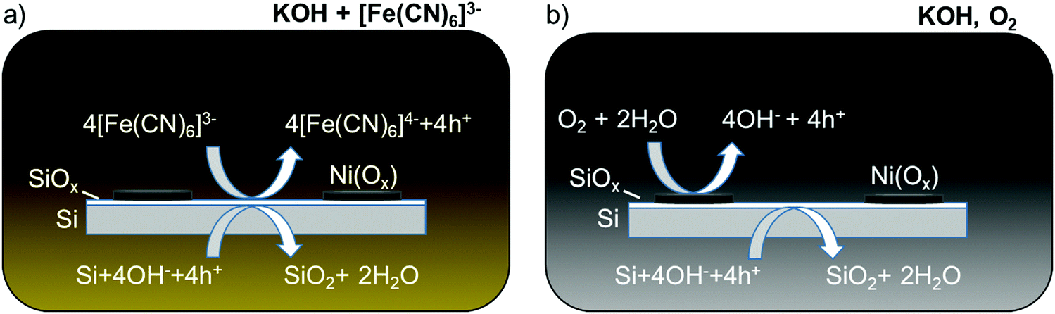 | ||
| Scheme 1 Schematic of two Si passivation mechanisms for a Si anode decorated with Ni(Ox) islands in alkaline electrolyte at open circuit in the dark. (a) [Fe(CN)6]3− is introduced as a protective electrolyte and acts as an oxidizing agent for Si.17 (b) Ni(Ox) uptakes O2 and catalyzes Si passivation. The electrode potential shifts positive, permitting holes from the Si valence band to react with the electrolyte and oxidize Si to SiO2. | ||
np+- and p+-Si electrodes decorated with arrays of 3–6 μm diameter Ni islands have been reported to exhibit extended stability (>24 h) in dark, open-circuit conditions and in the absence of protective electrolytes, even when >80% of the Si surface is exposed to the alkaline electrolyte.13,17 An understanding of the chemical and spatial details of the failure processes of Si photoanodes and of the fundamental reasons why unprotected Si photoanodes do not readily fail by corrosion could provide a basis for strategies to extend the operational lifetimes of photoanodes.
Herein we have investigated the mechanism by which Si can exhibit extended operation for water oxidation under day/night cycling in alkaline electrolytes as well as under other conditions where Si would be expected to rapidly etch and undergo pit corrosion. A hypothesis is that the presence of O2, along with an oxygen catalyst or a protective layer that can react with O2, produces a surface potential that drives formation of Si oxide. This process (Scheme 1b) is analogous to that of a protective one-electron redox-active oxidant in the electrolyte. We demonstrate that metal or metal oxide thin films such as Ni or NiOx, in the presence of O2, catalyze the dark, passive oxidation of Si in alkaline electrolytes. Such films can additionally induce local oxidation of exposed Si at pinholes or other film defects and thus lead to inherent defect tolerance of such interfaces. The catalyzed passivation of Si using Ni or NiOx thin films is thus compatible with previous investigations of Si/Ni-based photoanodes that were only evaluated under constant illumination. This behavior provides a strategy for extending the stability of photoelectrodes at exposed regions during periods when the surfaces would otherwise be subject to etching and/or associated corrosion at pinholes in protection layers.4,5
Results
Passivation and etching behavior of Si in KOH solution
Fig. 1 shows the voltammetric behavior of p+-Si(100) electrodes between −0.1 and 1.3 V vs. RHE in nominally 1 M KOH(aq) that had been saturated with 1 atm of either O2(g) or N2(g). The peaks of the anodic current at 0.17 V and 0.25 V vs. RHE for O2-saturated and N2-saturated Si samples, respectively, correspond to the passivation potential, EPP. The decrease in current at potentials positive of EPP indicates the formation of a passivating surficial Si oxide.19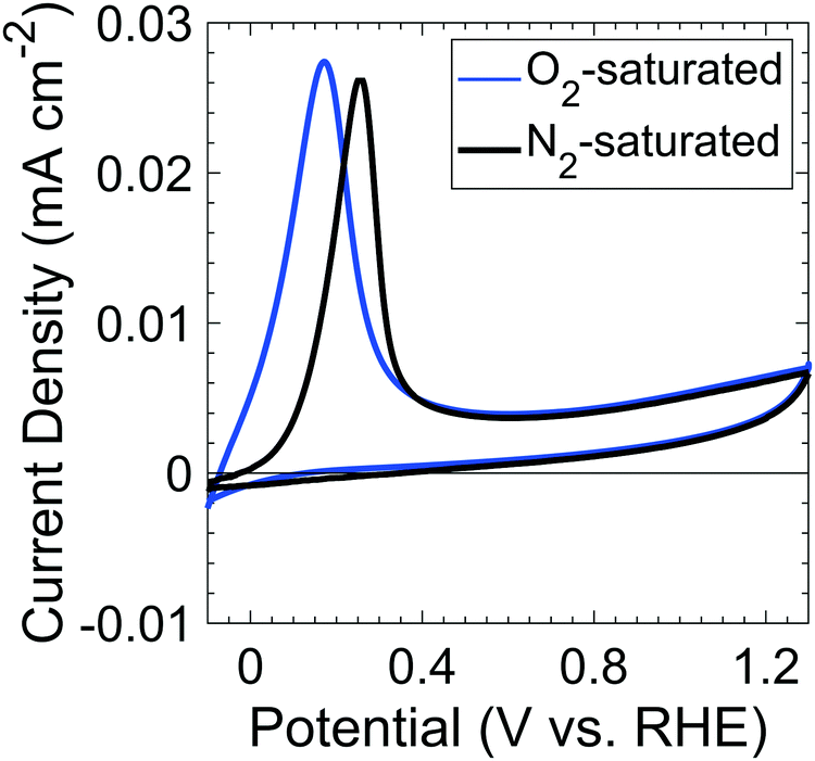 | ||
| Fig. 1 Cyclic voltammograms of p+-Si in O2- (blue) and N2- (black) saturated, 1 M KOH(aq) at a 1 mV s−1 scan rate in the dark. | ||
The dissolution rate, rD, of p+-Si(100) in 1 M KOH(aq) at open circuit (∼−0.1 V vs. RHE) was rD > 102 nm h−1 at room temperature.17 Fig. S1 (ESI†) shows rD as a function of the electrode potential. rD at a given potential was determined by etching exposed Si on an electrode patterned with a thermal oxide mask in 1 M KOH(aq), followed by removing the mask using buffered oxide etch, and measuring the resulting trench height using atomic force microscopy (Fig. S1c, ESI†). The rate decreased to 71.6 nm h−1 at 0.2 V vs. RHE and decreased further to a minimum of 1.7 nm h−1 at 0.5 V vs. RHE, consistent with the formation of a slowly dissolving SiOx layer at these potentials.20 The dissolution rate increased monotonically as the potential was increased to >0.5 V vs. RHE. Over the entire potential range, rD(E) correlated closely with the current density at the potential, E, of interest (Fig. S1b, ESI†). At low (<2 V) applied voltages, the Si dissolution behavior is consistent with expectations for a surface covered by a potential-dependent, steady-state thickness of Si oxide.21
Catalyzed passivation of p+-Si by Ni in O2-saturated strongly alkaline KOH(aq)
The morphology of etched Si(100) in KOH solution was used to provide information on the mechanism of the potential-dependent Si etching in the presence of various catalysts and surface layers.22 In 1 M KOH(aq), the Si(100) facets etch more rapidly than the Si(111) facets, leading to the formation of inverted pyramid-shaped pits on the Si(100) surface.10,19,23 Conversely, the SiOx passivation layer etches isotropically but at a rate <0.1 times that of Si, leading to facet-independent circular etch pits on oxide-covered Si surfaces.15,17Fig. 2 displays the open-circuit etching behavior of p+-Si(100), of p+-Si(100) with a thin film of 5 nm Ni (p+-Si(100)/Ni), and of p+-Si(100) with 60 nm of NiOx (p+-Si(100)/NiOx) in strongly alkaline 1 M KOH(aq) saturated with 1 atm of either O2(g) or N2(g). Electrodes tested in N2-saturated solution were used as a control during which O2 was purged from the cell. Unless otherwise stated, all of the films on Si were deposited as continuous thin films. Bare p+-Si(100) electrodes, in O2- or N2-saturated solutions, had open-circuit potentials, Eoc, < EPP with average potentials of Eoc = −0.07 and −0.11 V vs. RHE, respectively (i.e. more than 0.2 V negative of EPP). This low Eoc implies the direct dissolution of Si at open circuit regardless of whether O2 is present in the solution. In N2-saturated solution, p+-Si(100)/Ni or p+-Si(100)/NiOx surfaces initially exhibited Eoc ∼ 0.6 vs. RHE and Eoc ∼ 1.0 V vs. RHE, respectively; however, within a few hours the Eoc of both surfaces decreased to <0 V vs. RHE (Fig. 2b). In contrast, in O2-saturated solution, p+-Si(100)/Ni or p+-Si(100)/NiOx surfaces exhibited Eoc > 0.60 and >0.85 V vs. RHE, respectively, throughout the duration of the experiment (Fig. 2a).
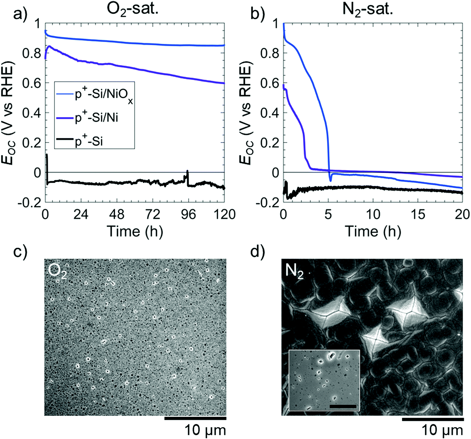 | ||
| Fig. 2 (a and b) Open-circuit potential (Eoc) vs. time in the dark of p+-Si(100) (black), p+-Si(100)/Ni (purple), and p+-Si(100)/NiOx (blue) electrodes in contact with (a) O2- and (b) N2-saturated 1 M KOH(aq). Ni and NiOx thin films were 5 nm and 60 nm thick, respectively. (c and d) Scanning electron micrographs of p+-Si(100)/Ni electrodes after immersion for 120 h in (c) O2-saturated and (d) N2-saturated 1 M KOH(aq). Energy-dispersive X-ray spectroscopy confirmed that Ni was no longer on the surface on (d). Inset in (d) shows p+-Si/Ni after immersion in N2-saturated KOH for 20 h, with the scale bar at 10 μm. | ||
The resulting etched electrode surfaces were characterized using scanning electron microscopy (SEM). After 120 h at open circuit in the O2-saturated electrolyte, SEM images of the p+-Si(100)/Ni surface showed circular etch pits (Fig. 2c). In contrast, after only 20 h at open-circuit in the N2-saturated electrolyte (Fig. 2d, inset) p+-Si(100)/Ni surfaces displayed inverted pyramids that visibly undercut the Ni film. Further, after 120 h continued undercutting led to a merging of the Si etch pits with the complete delamination of the Ni film on p+-Si(100)/Ni surfaces under N2, as confirmed by energy-dispersive X-ray spectroscopy (EDS, Fig. S2, ESI†). Qualitatively similar open-circuit etching behavior was also observed for p+-Si(100)/NiOx electrodes in either O2- or N2-saturated solutions (Fig. S3, ESI†). The cross section of the sample saturated in O2 showed that the underlying Si remained intact (Fig. S3c, ESI†).
To further investigate the potential-dependent behavior of the etching of Si electrodes, a p+-Si(100)/Ni electrode was held at E = −0.1 V vs. RHE in O2-saturated 1 M KOH(aq). After 20 h, SEM images showed inverted pyramids undercutting the Ni film (Fig. S4, ESI†), similar to the behavior of a p+-Si(100)/Ni sample in a N2-saturated solution.
Fig. S5 (ESI†) shows Eoc as a function of the thickness of the Ni film on p+-Si(100)/Ni electrodes in O2- and N2-saturated 1 M KOH(aq). In O2-saturated solutions, all electrodes showed initial values of Eoc between 0.7 and 0.8 V vs. RHE. Eoc remained in this range for the first hour, but after 120 h, Eoc was 0.29, 0.60, 0.64, and 0.73 V vs. RHE for 3 nm, 5 nm, 30 nm, and 60 nm thick Ni films on p+-Si(100), respectively. Fig. S6 (ESI†) shows SEM images of these electrodes after 120 h at open circuit in O2-saturated 1 M KOH(aq). Pronounced and spatially dense pinholes were produced on the p+-Si(100)/Ni electrode that had 3 nm of Ni, whereas the pinhole density decreased with increasing Ni thickness. The p+-Si(100)/Ni electrode with 60 nm of Ni exhibited much less undercutting of Ni. Regardless of the Ni film thickness, in N2-saturated 1 M KOH(aq), Eoc for the p+-Si/Ni electrodes decreased to <EPP within a few h of immersion, with 3 nm, 5 nm, and 30 nm thick Ni films requiring 1.6 h, 2.3 h, and 3.3 h, respectively, to produce Eoc < 0.2 V vs. RHE (Fig. S5b, ESI†).
Fig. S7 (ESI†) shows the behavior in O2-saturated 1 M KOH(aq) of p+-Si(100) electrodes coated with discrete, patterned Ni islands (μNi). A p+-Si electrode was patterned with an array of 60 nm thick, 3 μm diameter Ni islands (μNi) with a 7 μm pitch, p+-Si(100)/(μNi). This electrode exhibited a relatively steady potential of Eoc = 0.6 V vs. RHE for ∼120 h. Despite ∼86% of the Si surface being exposed to the electrolyte, the electrode did not exhibit characteristics of direct Si etching in the absence of illumination. In fact, SEM images showed no signs of inverted pyramid formation after the 120 h experiment, and the μNi array remained intact with minor radial undercutting (∼300 nm) of the μNi islands. The etching of the exposed Si surface was similar to the behavior exhibited by a Si/μNi electrode in KOH(aq) that contained a passivating electrolyte.17
Fig. S8 (ESI†) compares the electrochemical behavior of p+-Si/NiOx electrodes in O2- or N2-saturated 1 M KOH(aq). The Eoc of electrodes was measured for 6 h in 1 M KOH(aq), followed by chronoamperometry (CA) at 0.3 V vs. RHE for 1 h, after which cyclic voltammetry (CV) was performed from Eoc to +0.4 to −0.4 V vs. Eoc at 10 mV s−1. This cycle was repeated three times. At a potential that is positive of EPP, 0.3 V vs. RHE, reductive current was observed in both O2-saturated and N2-saturated solutions (Fig. S8b, ESI†).
As-deposited Ni films exhibit a relatively high overpotential for the OER in 1 M KOH(aq), in contrast to Fe-doped, Ni oxy-hydroxy (NiFeOOH) films.24Fig. 3 compares the open-circuit potentials in 1 M KOH(aq) for p+-Si(100) electrodes coated with either Ni or NiFeOOH films. Ni was converted to NiFeOOH by cycling the electrode potential between 0.3 and 1.63 V vs. RHE at 40 mV s−1 in 1 M KOH(aq) to oxidize the Ni and incorporate residual Fe from the solution.25 In both O2- and N2-saturated 1 M KOH(aq), p+-Si(100)/NiFeOOH electrodes initially displayed Eoc = 0.96 V vs. NHE, but Eoc decreased within <2 h of operation and converged towards Eoc values characteristic of as-deposited Ni films in both O2- and N2-saturated solutions. For the O2-saturated solution, Eoc = 0.65 V vs. RHE after 83 h, whereas for the N2-saturated solution, Eoc = 0.07 V vs. RHE after 4.3 h. The shift in Eoc of the Ni film in O2- or N2-saturated solution can be ascribed to changes in the relative amounts of oxidized Ni on the surface. The Ni oxy-hydroxy film readily converts to Ni oxide on the electrode surface at Eoc,26 because the potential for converting NiII into NiIII is positive of Eoc, lying in a potential region of ∼1.3 V vs. RHE.27
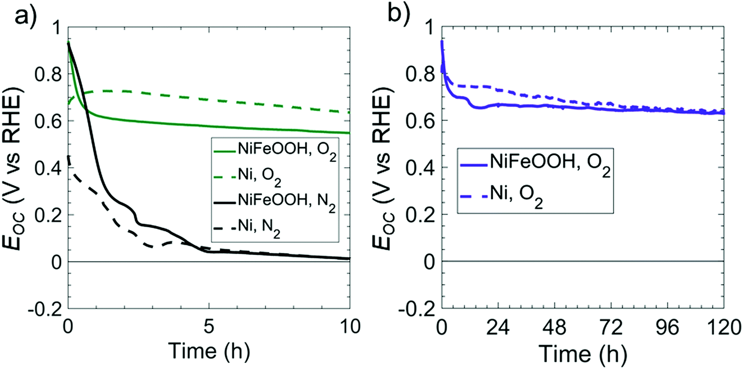 | ||
| Fig. 3 Comparison of the dark Eocvs. time behavior of p+-Si/Ni electrodes in 1 M KOH(aq) with and without initial cycling of the catalyst. (a) Open-circuit potential of 3 nm thick Ni films with (solid line) and without (dashed line) cycling in O2 (green) or N2 (black) saturated solution over a short time period. (b) Open-circuit potential of 30 nm thick Ni films over an extended time period. Cycled films had a potential applied over 20 cycles between 0.63 and 1.63 V vs. RHE at 40 mV s−1 to convert Ni to NiFeOOH. | ||
Si passivation using other catalysts
The open-circuit potential of p+-Si(100) electrodes coated with either Pt, Co, or TiO2 was also evaluated in O2-saturated KOH solution (Fig. S9, ESI†). Amorphous TiO2 was investigated due to its ability to provide a protective layer on Si,3,11,28 whereas Pt and Co were chosen due to their electrocatalytic activity for the ORR.29–31 p+-Si(100)/Pt electrodes displayed Eoc > 0.8 V vs. RHE for 120 h, with minimal undercutting of the film (Fig. S9b, ESI†). In contrast, within a day of immersion of p+-Si(100)/Co or p+-Si(100)/TiO2 surfaces, Eoc decreased from initial values of Eoc = 0.74 and Eoc = 0.49 V vs. RHE, respectively, to <0.25 V vs. RHE. After immersion, both types of electrodes exhibited inverted pyramid etch pits (Fig. S9c and d, ESI†), indicating that despite Eoc being slightly (<0.1 V) more positive than EPP, the rate of Si dissolution at open-circuit was greater than the rate of Si oxidation. No apparent correlation was observed between the catalytic activity of Pt, Co, Ni, and NiOx films for the ORR and the catalyzed passivation of Si (Fig. S10, ESI†).Photoelectrochemical characterization of catalytically passivated Si photoanodes subjected to simulated day/night cycling
Fig. 4 depicts the photoelectrochemical performance and stability of np+-Si(100)/NiOx photoanodes in 1 M KOH(aq) while undergoing cycling between 18 h intervals at open-circuit conditions in the dark (“night”) and 6 h intervals of 100 mW cm−2 illumination at E = 1.63 V vs. RHE (“day”). The photoelectrochemical cell was open to ambient air (∼0.2 atm O2) but was not continuously purged with O2. Throughout the duration of the experiment, the photoelectrode exhibited a light-limited current density of 31.0 ± 1.5 mA cm−2 during the day cycle (Fig. 4a), with small variations of photocurrent within individual day cycles consistently attributable to differing amounts of electrochromic darkening.32 Cyclic voltammograms collected at the beginning of each day cycle (Fig. 4b) were also essentially unchanged throughout the experiment. From 0 h to 114 h, the shift in potential (0.13 V shift negative at a current density of 1 mA cm−2) and the increase in current density for the NiIII/NiII redox peaks were consistent with an increase in catalytically active sites exposed to the electrolyte.6 Throughout every simulated night cycle, Eoc was >0.6 V vs. RHE (Fig. 4c), indicating that the Si was coated with a passivating oxide layer and confirming that the O2 concentration in the electrolyte was sufficient to maintain the passivating oxide. At the beginning of each simulated night cycle, Eoc started at ∼1.3 V vs. RHE and decreased to either ∼0.6–0.8 V vs. RHE in the first five night cycles or ∼1.2 vs. RHE during subsequent night cycles. The change in Eoc during each night cycle suggests that the catalytically active NiIII oxy-hydroxy film generated during the day likely converted to a NiII-based oxide during the night.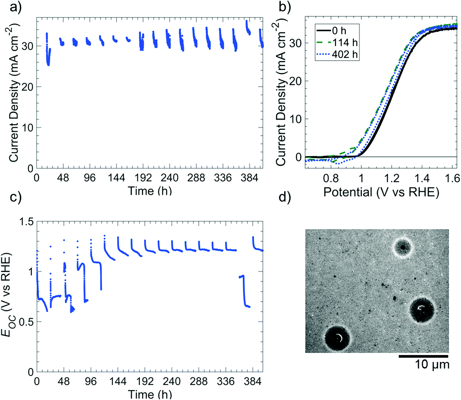 | ||
| Fig. 4 Stability and performance of np+-Si(100)/NiOx photoelectrodes subjected to cycling between simulated day and night conditions in 1 M KOH(aq). The deposited thickness of NiOx was 60 nm. (a) Chronoamperometric stability in 1 M KOH(aq) at 1.63 V vs. RHE. (b) Cyclic voltammetry of an electrode under simulated 1 sun illumination at 0 h (black, solid line), 114 h (green, dashed line), and 402 h of testing (blue, dotted line). The voltammetric scan rate was 40 mV s−1. For (a and b), photoelectrodes were measured for 6 h intervals under simulated 100 mW cm−2 of illumination provided by an ELH-type W-halogen lamp. (c) Open-circuit potentials of the photoelectrode in the dark for 18 h intervals. The electrolyte was replenished at 168 h and 378 h to account for evaporation. (d) Scanning electron micrographs of photoelectrodes after the stability test. | ||
After day/night cycling, SEM images revealed isotropically etched Si at pinholes in the photoelectrode (Fig. 4d). The images revealed that the NiOx film remained intact on the Si surface with some undercutting around the pinholes, as expected for Si/Ni electrodes in alkaline media.6 In the Si 2p X-ray photoelectron spectrum (XPS) of the photoelectrode surface that was subjected to day/night cycling, a weak SiO2 signal (102.6 eV binding energy), but no Si peak (∼99 eV), was present.33 This behavior confirms that the exposed regions of the surface were small areas of oxidized Si under pinholes, with the majority of the unoxidized Si being obscured by the NiOx film (Fig. S11, ESI†).
Under similar day/night cycling conditions, an np+-Si/TiO2/Ni photoanode in 1 M KOH(aq) did not exhibit catalyzed passivation despite the presence of a conformal layer of Ni on the TiO2 film (Fig. S12, ESI†). Instead, the electrode exhibited similar open-circuit behavior to that of p+-Si/TiO2 electrodes in the dark (Fig. S9, ESI†). Although the photoanode maintained performance for the first 216 h of the run, from 216 h to 312 h the photocurrent density decreased by ∼17%. Further, the bias sufficient to produce 10 mA cm−2 of photocurrent density under simulated 100 mW cm−2 illumination increased by 90 mV (Fig. S12c, ESI†), indicating substantial corrosion of the underlying np+-Si junction. Large (>20 μm) inverted pyramid etch pits that undercut the TiO2/Ni film were observed by SEM after 312 h of day/night cycling (Fig. S12d, ESI†).
Surface characterization of catalytically passivated p+-Si/Ni and np+-Si/NiOx
Fig. 5 compares the XPS data in the Ni 2p3/2 region for as-deposited p+-Si/Ni electrodes to p+-Si/Ni electrodes that had been immersed for 20 h in N2-saturated 1 M KOH(aq), as well as to p+-Si/Ni electrodes that had been immersed for 20 h in O2-saturated 1 M KOH(aq). The XPS emission at a binding energy of 852.4 ± 0.1 eV is associated with metallic Ni, whereas the emissions at binding energies of 853.5 ± 0.2 and 855.8 ± 0.2 eV are associated with phases of NiO and Ni(OH)2.34,35 The presence of NiOx peaks indicated that the oxidation of Ni proceeded at open circuit in 1 M KOH(aq) when O2 was present in solution, as suggested by the increase in the high-energy peak shaded in light blue (Fig. 5). Alternatively, after 20 h in N2-saturated 1 M KOH(aq), the composition of the Si surface was similar to that of the as-deposited electrode. After 120 h at open circuit in O2-saturated 1 M KOH(aq), atomic force microscopy (AFM) showed that the Ni surface morphology exhibited an increase in average surface roughness (Ra), from 0.2 to 1.8 nm, as a result of immersion in KOH(aq), and grain boundaries subsequently formed on the Ni surface (Fig. S13, ESI†). Cross-sections of the AFM illustrate the etch pit morphology caused by SiOx dissolution (Fig. S13c, ESI†).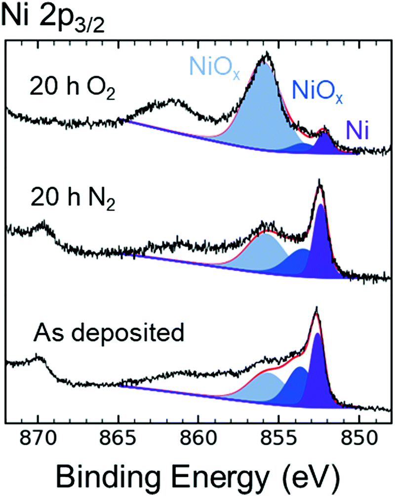 | ||
| Fig. 5 X-Ray photoelectron spectroscopic data in the Ni 2p3/2 region of p+-Si/Ni (5 nm thick) electrodes. Electrodes were measured as deposited and after 20 h at open circuit in either N2- or O2-saturated 1 M KOH(aq). Ni 2p3/2 emission was fitted with three peaks. The lowest energy peak at 852.4 eV (purple) is ascribable to Ni metal, and the higher energy peaks (blue and light blue) are assigned to NiO and Ni(OH)2. The y-axis is in arbitrary units. | ||
Fig. S14 (ESI†) shows the Ni 2p3/2 XPS data for as-deposited, np+-Si/NiOx photoelectrodes relative to np+-Si/NiOx photoelectrodes after 20 h in O2-saturated 1 M KOH(aq) at open circuit, as well as after extended day/night stability cycling (Fig. 4). Prior to XPS measurements, the open-circuit potentials for the latter two photoelectrodes were Eoc ∼ 0.6 V vs. RHE and Eoc ∼ 1.2 V vs. RHE, respectively. The XPS emissions at binding energies of 854.0 ± 0.2 and 855.8 ± 0.2 eV can be attributed to NiO, Ni(OH)2, and NiO(OH).34–36 The photoelectrode held at open circuit displayed a similar Ni 2p3/2 spectrum to that of the as-deposited NiOx film, indicating that a mix of nickel oxides was present on both surfaces. In contrast, the XPS data for the photoelectrode after extended day/night cycling revealed an emission at 855.8 eV but no lower energy emission (854.0 eV), indicating an increase in higher oxidation states of Ni after cycling.
Operation at near-neutral pH to inhibit the rate of SiOx dissolution
Fig. S15 (ESI†) displays the dissolution behavior of p+-Si(100) in O2-saturated, 0.5 M potassium borate buffer (K-Bi, pH 9.5), with the native oxide of p+-Si electrodes removed using buffered oxide etch prior to immersing the electrode in K-Bi. Analysis of the electrolyte by inductively coupled plasma mass spectrometry (ICP-MS) showed a negligible rate of Si dissolution for electrodes held either at open circuit or at 1.63 V vs. RHE (Fig. S15a, ESI†). A p+-Si(100) electrode that had been cycled immediately after immersion in K-Bi exhibited an anodic peak indicative of EPP at 0.31 V vs. RHE (Fig. S15b, ESI†). In contrast, a p+-Si electrode that was first held for 20 h at open-circuit in K-Bi did not exhibit an anodic peak, suggesting that a self-limited oxide had formed during immersion into the electrolyte (Fig. S15b, ESI†). XPS data confirmed the presence of SiOx after immersion of p+-Si in KBi at open circuit for 20 h (Fig. S16, ESI†). A p+-Si electrode that was similarly immersed in O2-saturated 1 M KOH(aq) for 20 h did not however exhibit a SiO2 peak in the Si 2p XPS region, indicating that Si dissolution dominated SiOx formation in KOH solution, but a relatively stable SiOx layer instead spontaneously formed at pH 9.5.Fig. 6 compares the performance of an np+-Si(100)/Ni photoanode under simulated day/night cycling in ambient (∼0.2 atm O2) conditions in 0.5 M K-Bi to the behavior under conditions analogous to those used for the KOH solutions. The steady light-limited photocurrent density was >24 mA cm−2 throughout the duration of each 120 h experiment. In 1 M KOH(aq), the photoanode exhibited qualitatively similar Eocvs. time behavior to that of the np+-Si/NiOx photoanode shown in Fig. 4, as expected due to the oxidation of surficial Ni to NiOx. In contrast, in K-Bi, Eoc decreased from ∼1.4 V to ∼1.0 V vs. RHE, followed by a comparatively gradual decline to Eoc ∼ 0.7–0.8 V vs. RHE, possibly due to a gradual conversion of Ni(Fe)OOH to NiO/Ni(OH)2. The photoanode exhibited a higher fill factor in 1 M KOH(aq) than in 1.0 M K-Bi(aq), with a ∼140 mV negative shift in initial onset potential and a reduction in series resistance from 15 Ω to 7 Ω as the pH was increased. These differences in performance were consistent with the increased overpotentials associated with the OER as the pH was decreased from highly alkaline conditions to near-neutral pH values.4,37 In both solutions, the photoanodes exhibited relatively unchanged voltammetric behavior throughout the 120 h experiment, but substantial changes to the surface morphology were nevertheless evident. Specifically, after cycling in 1 M KOH(aq), the photoanode surface was covered with circular etch pits, whereas no etch pits were observed on the photoanode that had been cycled in 1.0 M K-Bi(aq).
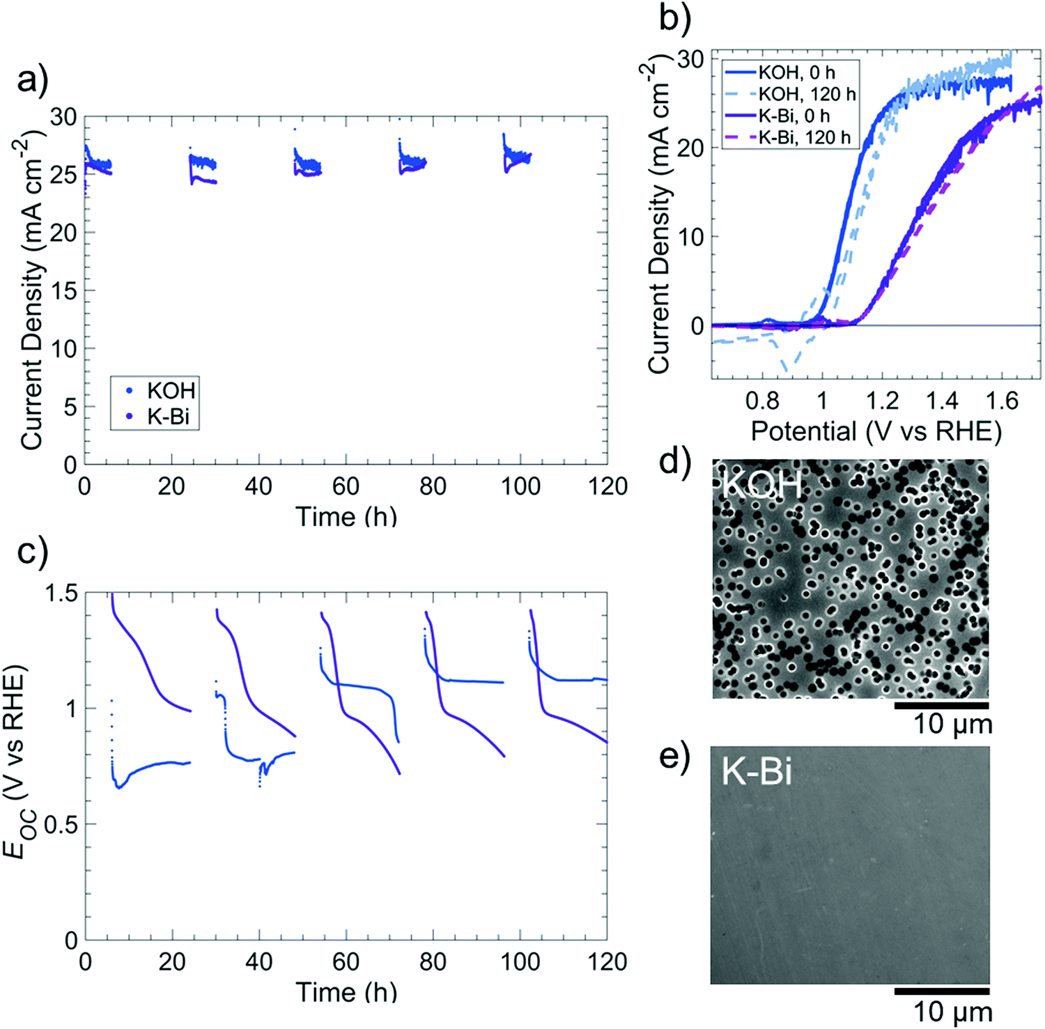 | ||
| Fig. 6 Comparison of the performance of np+-Si(100)/Ni (5 nm) photoelectrodes and of the etching behavior at strongly alkaline pH (1 M KOH(aq)) vs. near-neutral pH (0.5 M K-Bi(aq)) for electrodes subjected to cycling between simulated day and night conditions. (a) Chronoamperometric stability in 1 M KOH(aq) (blue) at 1.63 V vs. RHE and 0.5 M K-Bi(aq) (purple) at 1.73 V vs. RHE. (b) Cyclic voltammetry before (solid line) and after 120 h of testing (dashed line). The voltammogram scan rate was 40 mV s−1. For (a and b), photoelectrodes were under 100 mW cm−2 of illumination provided by an ELH-type W-halogen lamp for 6 h intervals, followed by collection of (c) open-circuit potentials of the photoelectrodes for 18 h intervals in the dark. (d and e) Scanning electron micrographs of photoelectrodes after stability tests in (d) 1 M KOH(aq) and (e) 0.5 M K-Bi(aq). | ||
Discussion
Proposed mechanism for catalytic passivation of Si using Ni-based thin films
Si passivation in alkaline media is achieved by poising the surface potential of the Si electrode sufficiently positive of EPP to oxidize any exposed Si. Previous work demonstrated this passivation effect using [Fe(CN)6]3− as a strong oxidant,17 whereas this work demonstrates that a Ni-based (or other) coating is sufficient to produce this effect in O2-saturated alkaline solution. Multiple Ni species (e.g. Ni, NiO, Ni(OH)2, and NiO(OH)) are capable of passivating Si; while the specific Ni species present influences the surface potential of the Si/Ni anode, the potential remains sufficiently positive to maintain Si passivation regardless of the Ni species (Fig. 2, 3 and Fig. S3, ESI†). The formation of passive oxides on the Si surface at open circuit in O2-saturated KOH with Ni-based coatings allows the underlying Si to be protected even if the Ni(Ox) film does not conformally cover the surface. For instance, 3 μm diameter μNi regions led to the passivation of regions of exposed Si that were microns away from the Ni islands (Fig. S7, ESI†).A combination of a Ni-based thin film and O2 in solution was required to facilitate Si passivation. Without the Ni(Ox) thin film, the Eoc of Si electrodes was ∼−0.1 V vs. RHE and thus below the anodic threshold for Si oxidation of EPP = 0.17 V vs. RHE (Fig. 1). At this potential, the observed inverted pyramid etch pits indicate rapid etching of Si(100) (Fig. 2d and Fig. S4, ESI†). Without O2 in the electrolyte, a Ni(Ox) film can initially define the surface potential of the electrode, likely due to the NiO, Ni(OH)2, and NiO(OH) species on the surface, but within a few hours the Eoc declined to <EPP and continued decreasing toward the open-circuit potential of Si (Fig. 2b). This decline indicates that the surface potential of the electrode is ultimately defined by Si dissolution. Conversely, Si(100) passivation in the presence of both O2 and a Ni(Ox) thin film is evident as shown by circular etch pits caused by isotropic SiO2 etching (Fig. 2c) and evidence of SiO2 at pinholes via XPS after testing (Fig. S11, ESI†).
The surface potential of the Si electrode at open circuit will equilibrate with the solution redox potential only if the solution couple can react at the Si surface. In the case of the O2/OH− (E0 = 1.23 V vs. RHE) redox couple, bare Si does not provide a low-energy pathway between the redox species. Thus, for a p+-Si electrode, the surface potential does not equilibrate with an O2-saturated 1 M KOH solution at open circuit. However, when the surface potential is controlled by a catalyst on the surface (p+-Si/Ni(Ox)), the potential responds to the presence of the O2 in the KOH(aq) solution.
The surface potential of p+-Si/Ni(Ox) electrodes is controlled by three factors: the redox couples within the NiOx film; interactions with solution redox couples; and dissolution of the bare Si. The Ksp of Ni(OH)2 is ∼10−15, so in strongly alkaline electrolytes only trace amounts of Ni(aq)2+ are present and solution Ni redox couples are not important.38 For a p+-Si/Ni(Ox) electrode under illumination or under anodic conditions, the Ni surface became more oxidized (Fig. 5). However, without O2 in the electrolyte, the Ni species on the surface of Si/Ni(Ox) electrode did not prevent the Eoc from decreasing to a value close to that of a bare Si electrode, below EPP (Fig. 2). Thus, for a p+-Si/Ni(Ox) electrode, the Ni solid-state redox couples alone did not dominate the electrode potential relative to Si dissolution. For p+-Si/Ni(Ox) in an O2-rich solution, the interactions between the Ni(Ox) on the surface of the electrode and the solution O2/OH− couple define the surface potential of the Si electrode, likely involving the oxidation and reduction of Ni species on the electrode surface.
When O2 is not present in the solution, few or no solution redox species are present. The solution potential is therefore largely undefined and cannot buffer the electrode potential despite the presence of a Ni(Ox) catalytic layer. Rather, the surface potential of the electrode is largely defined by Si oxidative dissolution, and as a result, the Eoc of the electrode rapidly decreases to negative of EPP.
The above observations suggest a correlation between the catalytic activity of the overlayer and Si passivation (Fig. S8c and S10, ESI†). This expectation is supported by the passivation of Si that was observed for p+-Si/Pt films in O2-saturated solutions (Fig. S9a and b, ESI†). The data are consistent with a model in which Si/Pt and Si/Ni surfaces are in communication with the O2/OH− solution couple. However, this simple correlation is not observed for Si covered by Co. The behavior of the Si/Co surfaces is consistent with complete air oxidation of the Co layer resulting in an electrically nonconductive overlayer,39 that precludes effective redox-catalyzed communication with the dissolved O2 to maintain the surface potential of the Si positive of EPP.
The Si/TiO2 surface is also electrically nonconductive, and hence leads to etching of the Si.40 The Si/TiO2/Ni interface has a buried Si surface, so changes in solution potential affect the Ni but do not affect the buried Si/TiO2 junction nor affect the surface potential of the Si.41
Assessing and mitigating SiOx dissolution
Although open-circuit Si passivation can extend device lifetimes by hundreds of hours for photoanodes subjected to day/night cycling in KOH solution,17 the gradual dissolution of SiOx will ultimately limit the overall device lifetime.13 Furthermore, the rate of SiOx dissolution is influenced by the surface potential of the Si that results from day and night conditions. Given the monotonic increase of the SiOx dissolution rate for potentials >0.5 V vs. RHE (Fig. S1a, ESI†), the day cycle when the potential is held at 1.63 V vs. RHE produces a larger etch rate than the night cycle, which results in a surface potential at the rest potential for the electrode in the dark. For a Si/Ni photoanode, the open-circuit potential shifted from Eoc ∼ 0.7 V vs. RHE (night) to ≥1.5 V vs. RHE (day) (Fig. 6c). Consequently, Si/Ni photoanodes undergoing day/night cycling exhibited more rapid SiOx etching (Fig. 6d) than Si/Ni electrodes held at open circuit (Fig. S6b, ESI†), as shown by the 1010 ± 70 nm and 380 ± 40 nm diameter etch pits, respectively.Several strategies have potential to further inhibit the dissolution rate of SiOx and extend the lifetime of the oxide-coated photoanodes. In one approach, the photoanode could be held at less positive operating potentials during the day cycles. For instance, an np+-Si/Ni photoanode in 1 M KOH(aq) (Fig. 6b) approaches the light-limited photocurrent density at an applied potential of ∼1.2 V vs. RHE rather than at 1.6 V vs. RHE. Consequently, operating at a less positive potential during the day cycles could inhibit the dissolution of the SiOx (Fig. S1a, ESI†). The oxide grown electrochemically could potentially be post-processed to a denser, more slowly dissolving oxide by thermal treatment, or could potentially be converted chemically to more inert materials such as Si nitrides, oxynitrides, carbides, or oxycarbides.
Operating the photoelectrode at pH 9.5 can also substantially inhibit dissolution of SiOx (Fig. S15, ESI†), although the lower pH introduces performance limitations due to increases in polarization losses and increased kinetic overpotentials for the OER. Additionally, the oxidized Ni film is partially soluble in K-Bi, and the associated loss of catalyst might consequently deleteriously reduce the device lifetime.42 The work herein clearly provides a systematic understanding of the durability of photoelectrodes by identifying the medium-term failure modes and mechanisms and then rationally implementing steps to mitigate the corrosion processes of concern.
Conclusions
Coating of Si with Ni or NiOx thin films prevented rapid Si dissolution in O2 saturated strongly alkaline electrolytes subjected to dark, open-circuit conditions. The combination of a Ni/NiOx catalyst and O2 in the electrolyte maintained the Si surface potential at >0.6 V vs. RHE, positive enough to catalyze the growth of SiOx on the Si surface at a rate faster than its dissolution. The O2 in the electrolyte plays an important role in driving the kinetics for Si passivation. Without O2 in the electrolyte the surface potential was defined predominantly by Si dissolution (∼−0.1 V vs. RHE).An np+-Si/NiOx photoanode undergoing day/night cycling exhibited stable performance for >408 h. The catalyzed passivation process reduced the rate of corrosion of exposed Si at pinholes in the NiOx film. Catalytic passivation of Si was observed with multiple phases of Ni–Ni, NiO, Ni(OH)2, and NiOOH – as well as with Pt. Although Si-based photoanodes are susceptible to eventual failure due to slow SiOx dissolution and subsequent undercutting of the protective film, this effect can be circumvented by leveraging the thermodynamic stability of SiO2 in pH 9.5 at the expense of an increased resistance and positive shifts in the onset potential. This work underscores the ability of well-established Si photoanode configurations to withstand rapid corrosion associated with patterns of diurnal insolation. Moreover, the work demonstrates the benefits of a systematic approach to increase the durability of photoelectrodes by identifying the dominant failure modes of the device and taking rational steps to mitigate such processes.
Experimental
Chemicals and materials
Unless otherwise stated, all chemicals listed were used as received, including potassium hydroxide (KOH, Macron Fine Chemicals, AR grade ≥85%), boric acid (H3BO3, Sigma-Aldrich, ≥99.5%), ammonium hydroxide (NH4OH, EMD Millipore Co., 28.0–30.0%), hydrochloric acid (HCl, EMD Millipore Co., 36.5–38%), hydrogen peroxide (H2O2, EMD Millipore Co., 30%), buffered oxide etchant (BOE, 6![[thin space (1/6-em)]](https://www.rsc.org/images/entities/char_2009.gif) :1 NH4F to HF, Transene Company, Inc.), boron nitride wafers (Saint-Gobain, BN-975 PDS), and Fumasep (Fuel Cell Store). Boron-doped, (100)-oriented p+-Si (0.001–0.005 Ω cm resistivity) and phosphorous doped, (100)-oriented n-Si (0.1–1.0 Ω cm resistivity) wafers were purchased from Addison Engineering, Inc. Ni, Co, and Pt sputtering targets were obtained from the Kurt J. Lesker Company. Tetrakis(dimethylamido)-titanium (TDMAT, Strem Chemicals) was used for atomic layer deposition (ALD). Photoresist (Shipley 1813), MCC primer 80/20 (Microchem Corp.), and MF-319 developer (Microchem Corp.) were used for photolithography. Ag paint (Ted Pella, Inc.), gallium-indium eutectic (Alfa Aesar, 99.99%), and epoxy (Loctite 9460) were used for preparation of electrodes. Deionized water with a resistivity ρ > 18.2 MΩ cm was obtained from a Barnstead Millipore purification system.
:1 NH4F to HF, Transene Company, Inc.), boron nitride wafers (Saint-Gobain, BN-975 PDS), and Fumasep (Fuel Cell Store). Boron-doped, (100)-oriented p+-Si (0.001–0.005 Ω cm resistivity) and phosphorous doped, (100)-oriented n-Si (0.1–1.0 Ω cm resistivity) wafers were purchased from Addison Engineering, Inc. Ni, Co, and Pt sputtering targets were obtained from the Kurt J. Lesker Company. Tetrakis(dimethylamido)-titanium (TDMAT, Strem Chemicals) was used for atomic layer deposition (ALD). Photoresist (Shipley 1813), MCC primer 80/20 (Microchem Corp.), and MF-319 developer (Microchem Corp.) were used for photolithography. Ag paint (Ted Pella, Inc.), gallium-indium eutectic (Alfa Aesar, 99.99%), and epoxy (Loctite 9460) were used for preparation of electrodes. Deionized water with a resistivity ρ > 18.2 MΩ cm was obtained from a Barnstead Millipore purification system.
Electrode preparation
np+-Si(100) photoelectrodes were fabricated via boron diffusion doping. Prior to doping, n-type Si wafers were cleaned by immersing in 5:1:1 H2O:NH4OH:H2O2 (by volume) at 75 °C for 15 min, followed by a 30 s etch in BOE to remove the oxide, immersing in 6:1:1 H2O:HCl:H2O2 (by volume) at 75 °C for 15 min, and etching once more in BOE for 30 s. After each step the wafers were rinsed with deionized water and dried under flowing N2(g). While the wafers were being cleaned, a tube furnace used for diffusion doping was heated to 950 °C for 30 min under a 5 L min−1 flow of O2 to oxidize the boron nitride wafers. The gas supply was switched from O2 to N2 for 30 min followed by cooling to 750 °C. The cleaned wafers were transferred to a tube furnace and placed a few mm from the oxidized boron nitride wafers. A p+-emitter was formed on the wafers after increasing the temperature to 950 °C under a 2 L min−1 flow of N2. To deglaze B2O3 from the surface, the sample was taken out and cooled before submerging in BOE for 2 min. Low-temperature oxidation was performed at 750 °C under 5 L min−1 for 30 min, followed by etching in BOE for 5 min to remove surface defects. The final sheet resistance was ∼70–80 Ω sq−1 as measured by a four-point probe (Jandel).
Ni, NiOx, Pt, and Co films were deposited onto np+-Si or p+-Si wafers using radio-frequency (RF) sputtering (AJA Orion sputterer). Prior to deposition, the p+-Si electrodes were cleaned and etched in BOE by the same process described above for n-type wafers. For deposition of Ni, Co, and Pt, 100 W was applied to the metal target under 20 sccm of Ar flow at a 5 mTorr chamber pressure until the desired thickness of material was obtained. NiOx films were deposited applying 120 W to the Ni target under 20 sccm Ar and 1 sccm O2 at 300 °C at a chamber pressure of 5 mTorr. The deposition rate was calibrated via profilometry (Bruker DektakXT Stylus profilometer) of the film that had been deposited onto a glass slide. Unless otherwise stated, the thickness of Ni, Co, and Pt were 5 nm whereas NiOx and Ni islands had thicknesses of 60 nm.
A carbide scribe was used to cleave off edges of samples from the wafers, to prevent shunting during electrochemical operation. In–Ga eutectic was scratched onto the back of each sample and attached to Sn-coated Cu wire using Ag paint. The wire was threaded through a glass rod and the edges of the sample were sealed to the glass using epoxy. The epoxy was cured overnight before testing the electrode the following day. Electrode areas were determined using ImageJ software in conjunction with an optical image of the electrode surface.
Electrochemical characterization
Electrodes were electrochemically tested in a three-electrode setup. A two-compartment cell separated by a Fumasep anion-exchange membrane was used for electrochemistry in KOH solution, whereas a two-compartment cell with the catholyte separated from the anolyte by a fritted glass tube was used for electrochemistry in 0.5 M K-borate buffer (K-Bi). Nominally 1 M KOH solutions were prepared by dissolving 56.0 g of hydrated KOH pellets into a total final volume of 1 L of deionized water, with the resulting pH measured as ∼13.6.43 K-Bi was prepared by mixing 1.0 M H3BO3(aq) and 0.5 M KOH(aq). The anolyte side of the cell was filled with 25 mL of electrolyte and the catholyte was filled to match the liquid height in the anolyte. Either O2 or N2 gas was bubbled into the anolyte as appropriate. A Hg/HgO reference electrode was used in KOH(aq) and a saturated calomel electrode (SCE) was used in K-Bi(aq). Reference electrodes were calibrated relative to the RHE using a Pt disk electrode in the respective electrolyte that was continually saturated with H2. The Hg/HgO and SCE electrodes had potentials in the range of 0.908–0.920 V vs. RHE and 0.772–0.785 vs. RHE, respectively, in 1 M KOH(aq) and 0.5 M K-Bi(aq), respectively. Ni wire was used as the counter electrode and was in contact with the catholyte. A MPG-2 potentiostat (Bio-Logic Science Instruments) was used for electrochemical measurements. For working electrodes using Ni as an OER catalyst, the film was initially activated via cyclic voltammetry by cycling 20 times between 0.63 and 1.63 V vs. RHE in KOH solution at 40 mV s−1 to incorporate Fe from solution and form NiFeOOH.For long-term photoelectrochemical stability experiments, the working electrode was placed <1 cm from the liquid surface and the electrolyte was replenished as necessary to maintain the liquid level. Illumination was provided with an ELH-type tungsten-halogen lamp and was calibrated to an equivalent power density of 100 mW cm−2 using a calibrated Si photodiode (Thorlabs). Photoelectrochemical stability was evaluated by cycling the electrode between day and night intervals within a 24 h period. Day cycles involved 6 h of continuous water oxidation under 100 mW cm−2 of simulated solar illumination at either 1.63 V vs. RHE in KOH or at 1.73 V vs. RHE in K-Bi, to ensure that the light-limited photocurrent density was reached in each case. Prior to each day cycle, the photoelectrodes were cycled between 0.63 V and either 1.63 V or 1.73 V vs. RHE in KOH(aq) and K-Bi(aq), respectively, at 40 mV s−1. Night cycles involved holding the photoelectrode at open circuit in the dark for 18 h.
Material characterization
Scanning electron microscopy (SEM) was performed using a FEI Nova NanoSEM 450 with accelerating voltages of 10 kV and a working distance of 5.0 mm. Energy-dispersive X-ray spectroscopy (EDS) was performed at accelerating voltages of 15 kV. Atomic force microscopy (AFM) was performed using a ScanAsyst-Air probe (Bruker) with a nominal tip radius of 2 nm in a Bruker Dimension Icon AFM using Peak Force Tapping mode. The Peak Force amplitude and frequency were set to 100 nm and 2 kHz, respectively. The image was measured using the software Nanoscope v9.7 and was analyzed using Nanoscope Analysis v1.9.X-Ray photoelectron spectroscopy (XPS) was performed using a Kratos Axis Ultra system at a base pressure of 1 × 10⁻⁹ Torr. Samples were irradiated with a monochromatic Al Kα source using X-rays (1486.7 eV) at 450 W. A hemispherical analyzer oriented normal to the sample surface was used to maximize the depth sensitivity. High-resolution spectra were acquired at a resolution of 25 meV with a pass energy of 10 eV. CasaXPS computer software was used to analyze the XPS data. The spectra were first calibrated by referencing the C 1s peak position to 284.8 eV, followed by peak fitting for Ni 2p3/2 to Ni subspecies.34,36 For simplicity, satellite and Ni 2p1/2 peaks of each subspecies were not used in peak fitting.6 The same peak width was used in all samples for a particular species. The XPS data were measured ex situ, which could potentially confound surface composition and oxidation states relative to those in the electrochemical measurements.
Inductively coupled plasma mass spectrometry (ICP-MS) data were collected using an Agilent 8800 Triple Quadrupole ICP-MS system to measure the extent of Si dissolution in 0.5 M K-Bi either at open circuit or at 1.63 V vs. RHE. To ensure that Si dissolution did not result from the borosilicate glass in the electrochemical cell, reference electrode, or working electrode, polypropylene and Teflon were used instead of glass. ICP-MS samples were collected periodically by removing 1 mL of solution at set time intervals. Before analysis, samples were diluted by a factor of 10 with 2% nitric acid. ICP-MS concentration standards were made by serial dilutions of a known concentration standard (Sigma-Aldrich) with 2% nitric acid. ICP-MS measurements were conducted using hydrogen as a reaction gas to eliminate interference due to atmospheric nitrogen in the measurement of Si. The total amount of dissolved Si from the electrodes was then calculated and normalized to the geometric electrode area.
Conflicts of interest
There are no conflicts to declare.Acknowledgements
This work was supported through the Office of Science of the U.S. Department of Energy (DOE) under award number DE-SC0004993 to the Joint Center for Artificial Photosynthesis, a DOE Energy Innovation Hub, and under award DE-SC0022087 from the Basic Energy Sciences Office of the DOE. Research was in part performed at the Molecular Materials Resource Center of the Beckman Institute.References
- M. X. Tan, P. E. Laibinis, S. T. Nguyen, J. M. Kesselman, C. E. Stanton and N. S. Lewis, Prog. Inorg. Chem., 1994, 21–144 CAS.
- D. Bae, B. Seger, P. C. Vesborg, O. Hansen and I. Chorkendorff, Chem. Soc. Rev., 2017, 46, 1933–1954 RSC.
- S. Hu, M. R. Shaner, J. A. Beardslee, M. Lichterman, B. S. Brunschwig and N. S. Lewis, Science, 2014, 344, 1005–1009 CrossRef CAS PubMed.
- M. J. Kenney, M. Gong, Y. Li, J. Z. Wu, J. Feng, M. Lanza and H. Dai, Science, 2013, 342, 836–840 CrossRef CAS PubMed.
- K. Sun, M. T. McDowell, A. C. Nielander, S. Hu, M. R. Shaner, F. Yang, B. S. Brunschwig and N. S. Lewis, J. Phys. Chem. Lett., 2015, 6, 592–598 CrossRef CAS PubMed.
- K. Sun, F. H. Saadi, M. F. Lichterman, W. G. Hale, H. P. Wang, X. Zhou, N. T. Plymale, S. T. Omelchenko, J. H. He, K. M. Papadantonakis, B. S. Brunschwig and N. S. Lewis, Proc. Natl. Acad. Sci. U. S. A., 2015, 112, 3612–3617 CrossRef CAS PubMed.
- X. Zhou, R. Liu, K. Sun, D. Friedrich, M. T. McDowell, F. Yang, S. T. Omelchenko, F. H. Saadi, A. C. Nielander, S. Yalamanchili, K. M. Papadantonakis, B. S. Brunschwig and N. S. Lewis, Energy Environ. Sci., 2015, 8, 2644–2649 RSC.
- X. Zhou, R. Liu, K. Sun, K. M. Papadantonakis, B. S. Brunschwig and N. S. Lewis, Energy Environ. Sci., 2016, 9, 892–897 RSC.
- P. Buabthong, Z. P. Ifkovits, P. A. Kempler, Y. Chen, P. D. Nunez, B. S. Brunschwig, K. M. Papadantonakis and N. S. Lewis, Energy Environ. Sci., 2020, 13, 4269–4279 RSC.
- D. Bae, S. Shayestehaminzadeh, E. B. Thorsteinsson, T. Pedersen, O. Hansen, B. Seger, P. C. K. Vesborg, S. Ólafsson and I. Chorkendorff, Sol. Energy Mater. Sol. Cells, 2016, 144, 758–765 CrossRef CAS.
- M. R. Shaner, S. Hu, K. Sun and N. S. Lewis, Energy Environ. Sci., 2015, 8, 203–207 RSC.
- H. G. G. Philipsen and J. J. Kelly, J. Phys. Chem. B, 2005, 109, 17245–17253 CrossRef CAS PubMed.
- K. Sun, Nicole L. Ritzert, J. John, H. Tan, W. G. Hale, J. Jiang, I. Moreno-Hernandez, K. M. Papadantonakis, T. P. Moffat, B. S. Brunschwig and N. S. Lewis, Sustainable Energy Fuels, 2018, 2, 983–998 RSC.
- K. Oh, C. Mériadec, B. Lassalle-Kaiser, V. Dorcet, B. Fabre, S. Ababou-Girard, L. Joanny, F. Gouttefangeas and G. Loget, Energy Environ. Sci., 2018, 11, 2590–2599 RSC.
- P. M. M. C. Bressers, S. A. S. P. Pagano and J. J. Kelly, J. Electroanal. Chem., 1995, 391, 159–168 CrossRef.
- X. H. Xia and J. J. Kelly, Electrochim. Acta, 2000, 45, 4645–4653 CrossRef CAS.
- H. J. Fu, I. A. Moreno-Hernandez, P. Buabthong, K. M. Papadantonakis, B. S. Brunschwig and N. S. Lewis, Energy Environ. Sci., 2020, 13, 4132–4141 RSC.
- D. R. Lide, CRC handbook of chemistry and physics, CRC press, 2004 Search PubMed.
- P. M. M. C. Bressers, J. J. Kelly, J. G. E. Gardeniers and M. Elwenspoek, J. Electrochem. Soc., 1996, 143, 1744–1750 CrossRef CAS.
- O. J. Glembocki, R. E. Stahlbush and M. Tomkiewicz, J. Electrochem. Soc., 1985, 132, 145–151 CrossRef CAS.
- J. W. Faust and E. D. Palik, J. Electrochem. Soc., 1983, 130, 1413–1420 CrossRef CAS.
- W. A. Pliskin and H. S. Lehman, J. Electrochem. Soc., 1965, 112, 1013–1019 CrossRef CAS.
- P. Allongue, V. Costa-Kieling and H. Gerischer, J. Electrochem. Soc., 1993, 140, 1018 CrossRef CAS.
- L.-A. Stern and X. Hu, Faraday Discuss., 2014, 176, 363–379 RSC.
- L. Trotochaud, S. L. Young, J. K. Ranney and S. W. Boettcher, J. Am. Chem. Soc., 2014, 136, 6744–6753 CrossRef CAS PubMed.
- L. F. Huang, M. J. Hutchison, R. J. Santucci, J. R. Scully and J. M. Rondinelli, J. Phys. Chem. C, 2017, 121, 9782–9789 CrossRef CAS.
- O. Diaz-Morales, D. Ferrus-Suspedra and M. T. M. Koper, Chem. Sci., 2016, 7, 2639–2645 RSC.
- M. Hannula, H. Ali-Löytty, K. Lahtonen, E. Sarlin, J. Saari and M. Valden, Chem. Mater., 2018, 30, 1199–1208 CrossRef CAS PubMed.
- S. Sui, X. Wang, X. Zhou, Y. Su, S. Riffat and C.-J. Liu, J. Mater. Chem. A, 2017, 5, 1808–1825 RSC.
- P. Yin, T. Yao, Y. Wu, L. Zheng, Y. Lin, W. Liu, H. Ju, J. Zhu, X. Hong, Z. Deng, G. Zhou, S. Wei and Y. Li, Angew. Chem., Int. Ed., 2016, 55, 10800–10805 CrossRef CAS PubMed.
- H. Abroshan, P. Bothra, S. Back, A. Kulkarni, J. K. Nørskov and S. Siahrostami, J. Phys. Chem. C, 2018, 122, 4783–4791 CrossRef CAS.
- A. Andersson, W. Estrada, C.-G. Granqvist, A. Gorenstein and F. Decker, Characterization of electrochromic dc-sputtered nickel-oxide-based films, SPIE, 1990 Search PubMed.
- D. S. Jensen, S. S. Kanyal, N. Madaan, M. A. Vail, A. E. Dadson, M. H. Engelhard and M. R. Linford, Surf. Sci. Spectra, 2013, 20, 36–42 CrossRef.
- M. C. Biesinger, B. P. Payne, L. W. M. Lau, A. Gerson and R. S. C. Smart, Surf. Interface Anal., 2009, 41, 324–332 CrossRef CAS.
- M. C. Biesinger, B. P. Payne, A. P. Grosvenor, L. W. M. Lau, A. R. Gerson and R. S. C. Smart, Appl. Surf. Sci., 2011, 257, 2717–2730 CrossRef CAS.
- A. P. Grosvenor, M. C. Biesinger, R. S. C. Smart and N. S. McIntyre, Surf. Sci., 2006, 600, 1771 CrossRef CAS.
- M. R. Singh, K. Papadantonakis, C. Xiang and N. S. Lewis, Energy Environ. Sci., 2015, 8, 2760–2767 RSC.
- S. V. Mattigod, D. Rai, A. R. Felmy and L. Rao, J. Solution Chem., 1997, 26, 391–403 CrossRef CAS.
- L. Smardz, U. Köbler and W. Zinn, J. Appl. Phys., 1992, 71, 5199–5204 CrossRef CAS.
- P. Nunez, M. H. Richter, B. D. Piercy, C. W. Roske, M. Cabán-Acevedo, M. D. Losego, S. J. Konezny, D. J. Fermin, S. Hu, B. S. Brunschwig and N. S. Lewis, J. Phys. Chem. C, 2019, 123, 20116–20129 CrossRef CAS.
- M. H. Richter, W.-H. Cheng, E. J. Crumlin, W. S. Drisdell, H. A. Atwater, D. Schmeißer, N. S. Lewis and B. S. Brunschwig, Chem. Mater., 2021, 33, 1265–1275 CrossRef CAS.
- K. Sun, R. Liu, Y. Chen, E. Verlage, N. S. Lewis and C. Xiang, Adv. Energy Mater., 2016, 6, 1600379 CrossRef.
- S. Hu, N. S. Lewis, J. W. Ager, J. Yang, J. R. McKone and N. C. Strandwitz, J. Phys. Chem. C, 2015, 119, 24201–24228 CrossRef CAS.
Footnote |
| † Electronic supplementary information (ESI) available. See DOI: 10.1039/d1ee03040j |
| This journal is © The Royal Society of Chemistry 2022 |