
Improved performance and stability of perovskite solar modules by interface modulating with graphene oxide crosslinked CsPbBr3 quantum dots†
Shujing
Zhang‡
a,
Rui
Guo‡
 a,
Haipeng
Zeng
a,
Yang
Zhao
a,
Xingyue
Liu
b,
Shuai
You
a,
Min
Li
a,
Long
Luo
a,
Monica
Lira-Cantu
c,
Lin
Li
a,
Fengxiang
Liu
a,
Xin
Zheng
a,
Guanglan
Liao
b and
Xiong
Li
*a
a,
Haipeng
Zeng
a,
Yang
Zhao
a,
Xingyue
Liu
b,
Shuai
You
a,
Min
Li
a,
Long
Luo
a,
Monica
Lira-Cantu
c,
Lin
Li
a,
Fengxiang
Liu
a,
Xin
Zheng
a,
Guanglan
Liao
b and
Xiong
Li
*a
aMichael Grätzel Center for Mesoscopic Solar Cells (MGC), Wuhan Photoelectric National Research Center (WNLO), Huazhong University of Science and Technology, Wuhan 430074, Hubei, China. E-mail: xiongli@hust.edu.cn
bState Key Laboratory of Digital Manufacturing Equipment and Technology, Huazhong University of Science and Technology, Wuhan 430074, Hubei, China
cCatalan Institute of Nanoscience and Nanotechnology (ICN2), CSIC and the Barcelona Institute of Science and Technology (BIST), Campus UAB, Bellaterra, Barcelona 08193, Spain
First published on 16th November 2021
Abstract
Perovskite solar cells (PSCs) are one of the most prominent photovoltaic technologies. However, PSCs still encounter great challenges of scaling up from laboratorial cells to industrial modules without serious performance loss while maintaining excellent long-term stability, owing to the resistive losses and extra instability factors that scale quadratically with the device area. Here, we manifest a concept of multifunctional interface modulation for highly efficient and stable perovskite solar modules (PSMs). The advisably designed multifunctional interface modulator GO/QD crosslinks the CsPbBr3 perovskite quantum dots (QDs) on the conductive graphene oxide (GO) surfaces, which significantly improve charge transport and energy band alignment at the perovskite/hole transporting layer interface to reduce the charge transport resistance while passivating the surface defects of the perovskite to inhibit carrier recombination resistive losses. Moreover, the GO/QD interlayer acts as a robust permeation barrier that modulates the undesirable interfacial ion and moisture diffusion. Consequently, we adopt a scalable vacuum flash-assisted solution processing (VASP) method to achieve a certified stabilized power output efficiency of 17.85% (lab-measured champion efficiency of 18.55%) for the mini-modules. The encapsulated PSMs achieve over 90% of their initial efficiency after continuous operation under 1![[thin space (1/6-em)]](https://www.rsc.org/images/entities/char_2009.gif) sun illumination and the damp heat test at 85 °C, respectively.
sun illumination and the damp heat test at 85 °C, respectively.
Broader contextPerovskite solar cells (PSCs) as a promising and competitive candidate have attracted tremendous attention in the photovoltaic (PV) field due to their unprecedented gains, the lab-scale certified efficiencies of which are over 25%. However, scaling up from laboratorial cells to industrial modules without serious performance losses while maintaining excellent stability remains a major bottleneck for the commercialization of PSCs. The parasitic resistive losses and instability factors scale steeply with the increased device area. We designed a crosslinked graphene oxide/CsPbBr3 quantum dot (GO/QD) composite as a multifunctional interfacial modulator to synergistically optimize the carrier management and hinder the unwanted interfacial ion and moisture diffusion within the perovskite solar modules. Consequently, the PSMs achieved a remarkable efficiency of 18.55% (certified 17.85%) on 6 × 6 cm2 substrates and exhibited outstanding stability under illumination and thermal conditions. |
Introduction
Perovskite solar cells (PSCs) have attracted extensive research interest as the most promising candidates for the next generation of photovoltaic (PV) technologies. The certified power conversion efficiencies (PCEs) of laboratory-scale (≈0.1 cm2) PSCs have rapidly surpassed 25%, and the stability has progressed significantly due to the composition and interlayer engineering. However, owing to resistive losses and extra instability factors which scale steeply with the active cell areas, the PSCs suffer from low efficiencies and poor long-term stability upon scaling-up to mini-modules whose aperture areas are defined between 10 cm2 and 200 cm2, thereby greatly hampering the commercialization of the emerging photovoltaic (PV) technologies.1In principle, achieving high-efficiency PV devices should require low series resistance (Rs) and high shunt resistance (Rsh). However, scaling up processes boost the possibility of shunts created by morphological imperfections in the perovskite layer (e.g., defects, voids/pinholes, and impurities) and hence enhance the charge carrier recombination rate in PSCs.2 Whereas the series resistive losses, resulting from a poor interfacial contact and relatively low charge transfer rate at the interface as well as poor conductivity of the corresponding active materials, scale quadratically with the photocurrent.3,4 Up to now, many scalable fabrication techniques, such as a vacuum flash-assisted process method (VASP), doctor-blade, slot-die coating, screen printing, vacuum deposition, air blowing, spray-coating, and additive engineering, have been developed to improve the perovskite film quality with high smoothness and free of pinholes, which is beneficial for reducing resistive losses.5–15 Based on the development of scalable deposition methods, the certified PCEs of mini-PSMs are in the range of 10.0–18.6%, which are still much lower than those of commercial solar modules based on other PV technologies.16–19 Hence, recent research focuses on optimizing charger carrier management to minimize parasitic resistive losses from shunt and series resistances to further improve the PCEs of PSMs. Han et al. introduced bridge-jointed graphene oxide nanosheets to improve the carrier mobility of the charge transporting layer (HTL), obtaining a certified efficiency of 15.3%.20 Zhao et al. utilized dual-chloride passivation by MACl and excessive PbCl2 to minimize the non-radiative recombination and local carrier transport losses, achieving a 17.88% certified PCE for PSMs.21
In addition to upscalability and efficiency, the long-term stability of PSMs is another important restriction for commercialization.22 The fabrication complexity of PSMs increases the extra instability factor induced by laser-scribing.23 The perovskite film is scribed and partially exposed to a metal electrode or air, providing additional pathways for iodide diffusion and moisture ingression in PSMs. However, studies on improving the stability of PSMs were very rare until recently. Han et al. devised an iodide diffusion barrier to suppress degradation from laser-scribed lines.24 Liu et al. employed a holistic approach by modifying all the correlative layers and interfaces to improve the stability of mini-modules.25 Huang et al. added excessive AX to compensate for defects with improved photostability.19 Nevertheless, up to now, scalable strategies to simultaneously improve the efficiency and stability of PSMs are very limited.
Here, we report a multifunctional interfacial modulation strategy to realize stable and efficient PSMs by both optimizing the charge transport/carrier recombination and hindering the adverse diffusion of ions/molecules within the solar cells. Perovskite quantum dots (QDs) with adjustable energy bands are promising interface modulators, which have been proven to be of prime importance for the photovoltaic performance of PSCs by optimizing the interfacial charge-carrier transport and collection.26–28 However, the electrical properties of perovskite QDs hinder the charge transport due to the insulating ligands and isolated distribution. On the other hand, incorporating carbon materials into PSCs has been proven to be revolutionary to alleviate PSC degradation by suppressing the undesirable interfacial ion and moisture diffusion.29 To take advantage of these collective effects exerted by QDs and GO, herein we introduced a synergistic interface modulation strategy by crosslinking CsPbBr3 QDs with the conductive graphene oxide (GO) through a Pb–O bond and forming a charge transport network to improve the electrical properties of the interlayer. The crosslinked GO/QDs composite interlayer provided both excellent charge transport and effective interfacial passivation, resulting in decreased parasitic resistive losses. We fabricated highly efficient perovskite mini-modules and achieved a stabilized power output efficiency of 17.85% with the VASP method as certified by the National Institute of Metrology (NIM) of China, which is one of the highest certified PCEs among the reported efficiencies for mini-scale PSMs as shown in Table S1 (ESI†). Moreover, the GO/QD composite layer serves as a barrier that can prevent moisture penetration and internal iodide (I−) and Au migration. The encapsulated PSMs retain 91% of their initial PCE at 85 °C with 60% relative humidity for 1000 h or 90% of their initial PCE under continuous 1-sun irradiation for 1000 h.
Results and discussion
The synthesis process of the crosslinked GO/(CsPbBr3 QD) composite is illustrated in Fig. 1a. Highly crystalline and cubic-structured QDs (Fig. S1a, ESI†) with an average size of 8.8 ± 4 nm (Fig. S1b, ESI†) were synthesized by hot injection.30 The solvent-exfoliated GO sheets composed of a single layer (Fig. S1c and d, ESI†) were added into the as-synthesized QD colloid solution to form the GO/QD composite material (Fig. S1e, ESI†). The transmission electron microscope (TEM) and corresponding energy-dispersive X-ray (EDX) mappings of Cs, Pb, Br, and C confirmed the existence and uniform dispersion of the CsPbBr3 QDs on GO. In the GO/QD composite material, the crystal structure of the QDs remained unchanged (XRD, Fig. S2, ESI†). Conductive GO partially replaced insulating ligands (oleic acid, oleylamine) and crosslinked isolated QDs (FTIR, Fig. S3, ESI†), decreasing the charge transport resistance. The UV-visible absorption spectra and the steady-state photoluminescence (PL) spectra of CsPbBr3 QDs and GO/(CsPbBr3 QDs) films were measured (Fig. 1b). While both the films exhibited nearly identical absorption spectra with onset at 510 nm (2.43 eV), the PL peak intensity of the GO/QDs film was considerably less than that of the QDs film, which implied efficient charge transport pathways from the QDs to the GO sheets due to the p-type nature and conductivity of GO. The electrical conductivity properties of the QDs film and GO/QDs film were assessed from I–V measurement with the structure of the ITO/QDs film or (GO/QDs) film/Au. The GO/QDs film showed a higher current density at the same bias voltage than that of the QDs film, indicating improved conductivity. (Fig. 1c). Simultaneously, the crosslinked GO/QDs films exhibited much higher humidity and thermal stability than pure QD, which is suitable for a stable interface modulator (Fig. S4, ESI†). | ||
| Fig. 1 (a) Synthesis process of the GO/QDs composite materials. (b) Typical optical absorption spectra (red line) and PL spectra (blue line) of QDs/GO and QDs films. (c) I–V curves for QDs and GO/QDs films. | ||
The well-dispersed GO/QDs composite was deposited on the FAPbI3-based perovskite film by a solution-processing method as a thin interlayer. Cross-section EDX mapping of the Cs signal confirmed the existence of the GO/QDs interlayer with a thickness of ∼25 nm (Fig. 2a). The GO/QDs composite was dense and evenly distributed on top of the perovskite layer (Fig. S5, ESI†), and the crystal structure of the QDs remained unchanged (Fig. S6, ESI†). The atomic force microscopy (AFM) images of the perovskite film with the GO/QDs interlayer were smoother than the pristine perovskite film (Fig. S7, ESI†), in line with the scanning electron microscopy (SEM) images (Fig. S5, ESI†). The root-mean-square roughness (Rq) values were 29.5 and 18.2 nm for the perovskite films without (pristine) or with the GO/QDs interlayer, respectively. The smoother surface of the perovskite film with GO/QDs was beneficial for the formation of a high-quality HTL, resulting in a non-porous and smooth Spiro-MeOTAD layer, which is beneficial to minimize the resistive losses (Fig. S8, ESI†). Water contact angles increased from 52.94° (pristine) to 79.80° (perovskite films with GO/QD interlayer), as shown in Fig. S7 (ESI†) inset, verifying that the perovskite films with GO/QDs were more hydrophobic to effectively protect the perovskite layer from moisture incursion.
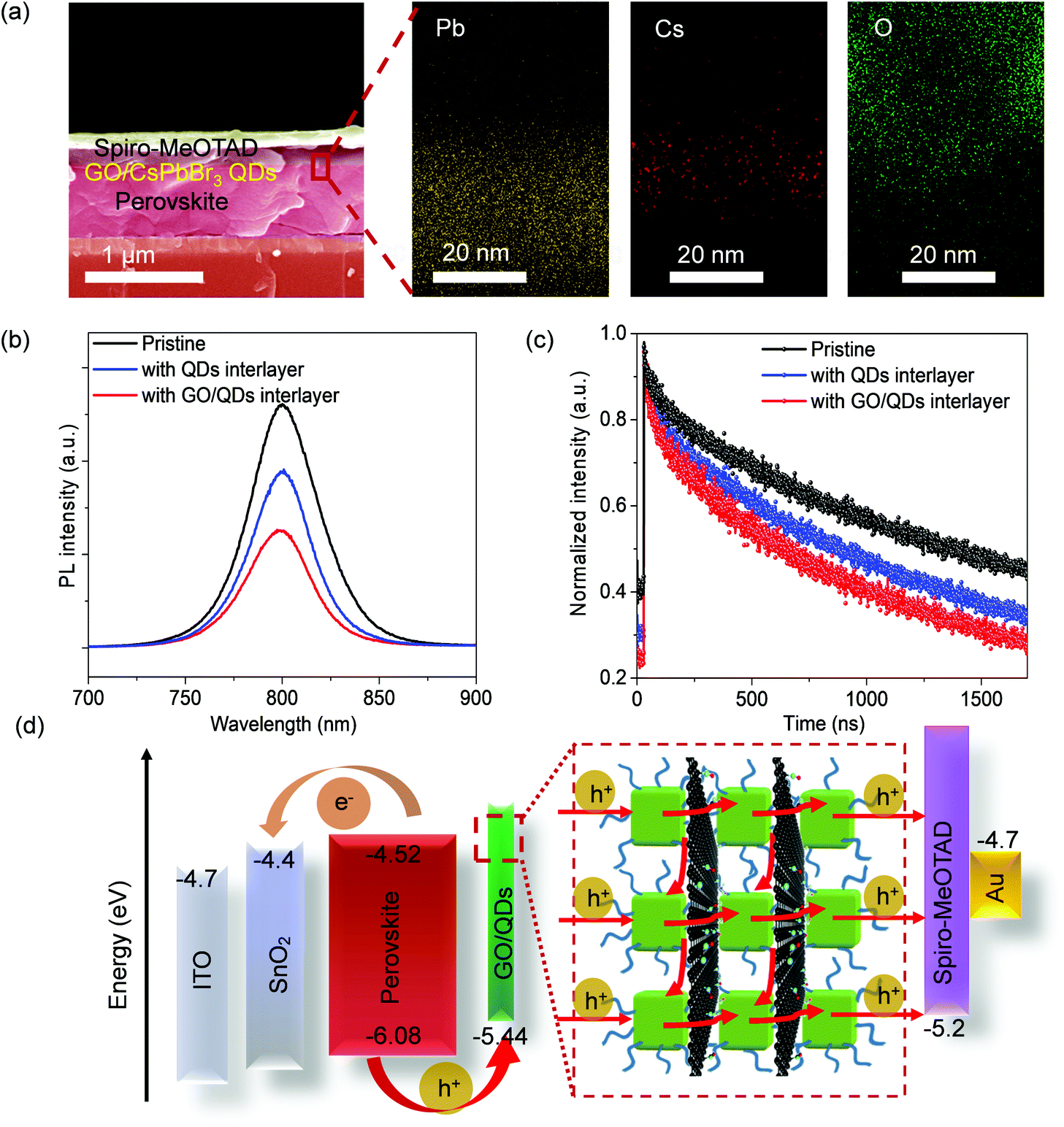 | ||
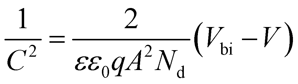
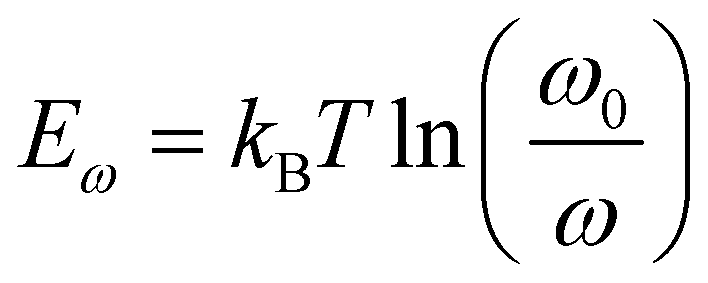
| Fig. 2 (a) Cross-section SEM image and EDX mapping of the Spiro-MeOTAD-based PSCs device with a GO/QDS interlayer. The Cs signal indicated the presence of QDs and the O signal represented the existence of Spiro-MeOTAD, GO, and ligands (oleic acid). (b) PL and (c) TRPL spectra of the pristine perovskite films, perovskite/QD film, and perovskite/(GO/QDs) film, respectively. (d) The energy level and transmission mechanism diagram of PSCs. | ||
The electronic structure of the GO/QDs interlayer was investigated using ultraviolet photoelectron spectroscopy (UPS) (Fig. S9, ESI†). The upward valence band (EV) of the GO/QDs composite offered more favorable band alignment with the underneath perovskite than that of the QDs interlayer (Fig. S10, ESI†). Steady-state PL of the pristine perovskite film, perovskite with QDs, and perovskite with GO/QDs was measured to confirm the effect of the interlayers on charge transport. The PL intensity of the perovskite with QDs declined compare to that of the pristine perovskite, while the PL intensity of the perovskite with GO/QDs declined most among the three (Fig. 2b). Time-resolved PL (TRPL) spectra were collected to quantify the carrier lifetime (Fig. 2c and Table S2, ESI†). The average carrier lifetimes (τave) of the perovskite film with the GO/QDs interlayer showed the shortest PL value (1043.4 ns) among those of the three samples, indicating the most efficient charge transport.31 These results confirmed the GO/QD interlayer had a unique ability to promote charge transfer, which was critical for high-efficiency PSMs. Fig. 2d shows the energy band diagram of the device with GO/QDs interlayer. The photogenerated holes in the perovskite layer are extracted by the QDs. However, the organic ligands with poor conductivity and relatively isolated QDs hamper charge transport in the QDs interlayer. GO partially replaces the organic ligands and crosslinks the isolated QDs to form a charge transport network, improving the conductivity of the interlayer and decreasing transport resistance.
Transient photovoltage decay (TPV) and transient photocurrent decay (TPC) were used to study the carrier recombination lifetime and charge extraction lifetime of the pristine PSC device, PSC device with QDs, and PSC device with GO/QDs (Fig. 3a and b). Among the three, the device with GO/QDs achieved the longest carrier recombination lifetime (124 μs) and the shortest charge extraction time (0.878 μs), indicating suppressed charge carrier recombination and enhanced carrier extraction efficiency.32 These results indicate that the GO/QDs interlayer plays a dominant role in maintaining the high VOC and fill factor (FF). Under different light intensities, we observed the change of the VOC of the devices with different interlayers to research the carrier recombination behavior (Fig. 3c). The PSC with the GO/QD interlayer showed a slope of 0.98 kT q−1, which was the lowest among the three (QDs, 1.15 kT q−1vs. Pristine, 1.28 kT q−1). This indicates that the PSCs with GO/QDs substantially reduces trap-assisted recombination and boosts charge extraction.8,33,34 Mott–Schottky plots were carried out to investigate the interfacial carrier density using the following eqn (1) (Fig. 3d):35
 | (1) |
× 1011cm−3) was the lowest, suggesting the lowest charge accumulation at the perovskite/(GO/QD composite) interface, which best-reduced the carrier recombination (Table S3, ESI†).35,36 To quantify the trap density of states (tDOS), which was derived from the angle frequency-dependent capacitance measurement (Fig. S11a, ESI†), thermal admittance spectroscopy (TAS) was carried out and shown in Fig. 3e. The trap density was calculated from eqn (2) and (3):37,38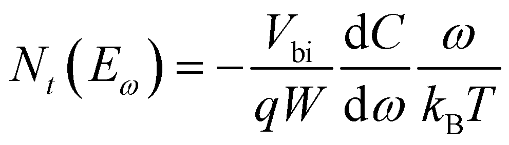 | (2) |
 | (3) |
× 1017 cm−3) whereas the pristine device and device with QDs showed a trap density of 2.08 × 1017 cm−3 and 1.68 ×1017 cm−3, respectively. The reduction in trap density confirmed the minimum interfacial carrier recombination in the device with the GO/QD interlayer and eventually resulted in an enhanced open-circuit voltage (VOC). To quantitatively calculate the trap density variation, the dark current–voltage characteristic of space-charge-limited-current (SCLC) with hole-only device architecture (ITO/PTAA/perovskite/interface layer/Spiro-MeOTAD/Au) was constructed (Fig. S11b, c, and d, ESI†).32 The trap density (ntrap) can be calculated using eqn 4:41–43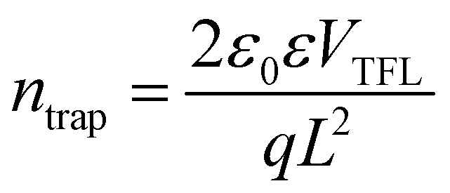 | (4) |
× 1015 cm−3, 4.33 ×1015 cm−3, and 3.68 ×1015 cm−3 for the pristine device, QDs-containing, and GO/QDs-containing samples, respectively, indicating that the GO/QDs interlayer could exert a particularly pronounced effect on passivating defects located on the perovskite surface. The electrical impedance spectroscopy (EIS) was conducted to investigate the transport resistance (Rtr) and recombination resistance (Rrec) in the PSCs (Fig. 3f).44 It showed two separate arcs, equivalent to the resistance and capacitive components. The first arc in the high-frequency region was associated with the transport impedance, whereas the second arc at the low-frequency region was associated with recombination impedance in the device. The devices with the GO/QDs interlayer showed the smallest Rtr and the largest Rrec among the three devices, indicating effective carrier extraction and the suppressed carrier recombination, which is in agreement with the observations discussed above.45
 | ||
| Fig. 3 (a) Charge carrier lifetime from normalized SCLC decay and (b) normalized transient photocurrent (TPC) decay in different interlayer-based perovskite solar cells. (c) The VOCvs. light intensity curves of PSCs. (d) Mott–Schottky plots at 10kHz. (e) The calculated trap density of states (tDOS) distribution of the devices at room temperature. (f) EIS analysis of PSCs without (Pristine) and with QDs or GO/QDs interlayer. | ||
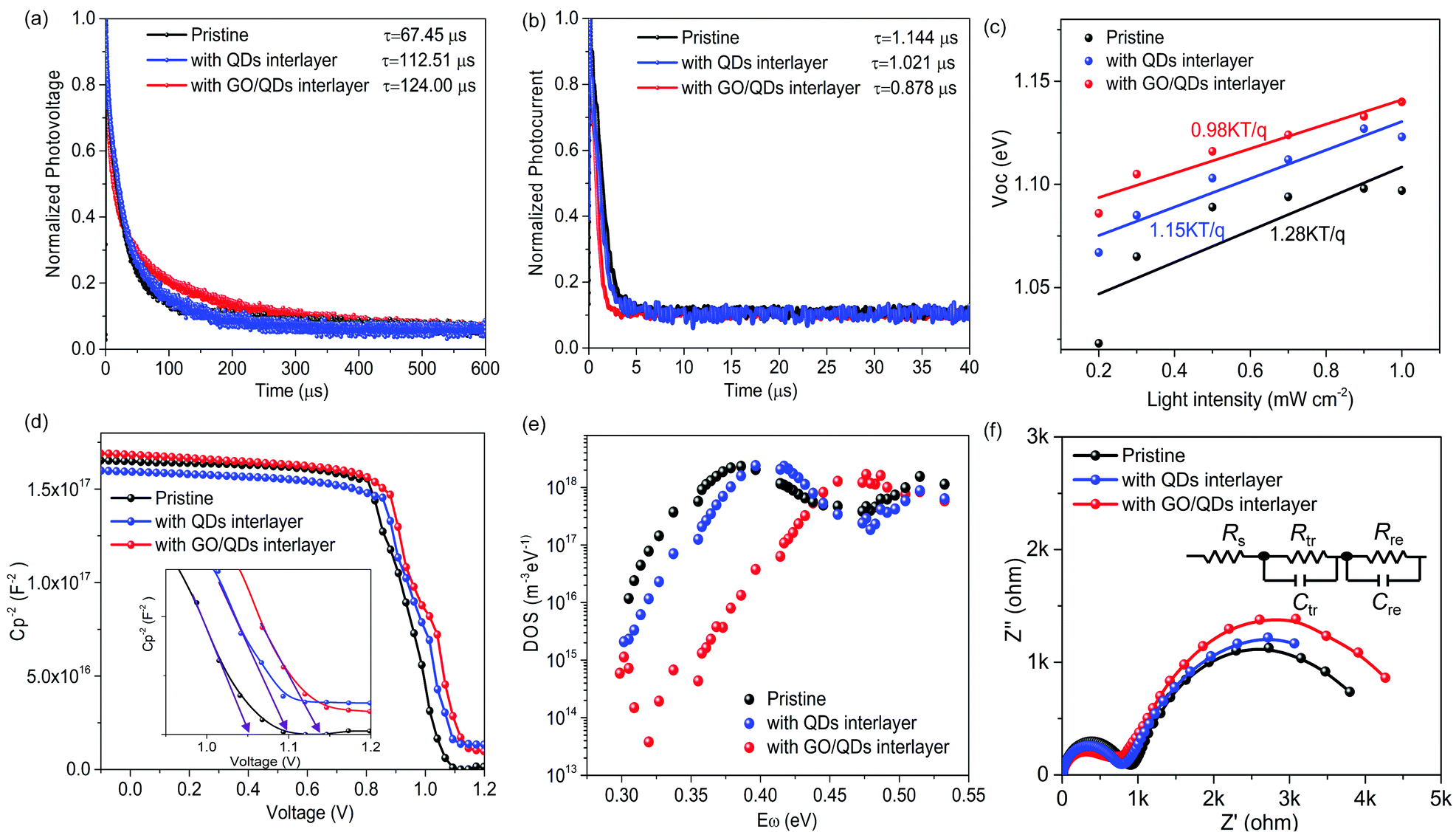
Typical current density–voltage (J–V) curves of the large-area PSCs (≈1 cm2) using the VASP method and with Spiro-MeOTAD as HTL are shown in Fig. 4a and Table 1. The pristine device provided a PCE of 19.58% with an open-circuit voltage (VOC) of 1.09 V, a short-circuit current density (JSC) of 23.56 mA cm−2, and a fill factor (FF) of 0.76. While PSCs with QDs and GO/QDs delivered champion PCEs of 20.59% and 21.42%, respectively, implying that the CsPbX3 QD component rather than the GO segment in the GO/QDs interlayer plays the dominant effect on the photovoltaic performance improvement (Table S4, ESI†). The maximum steady-state photocurrent and the corresponding power measurements were further conducted (Fig. 4b). The device with the GO/QDs interlayer yielded a PCE of 21.19% with a photocurrent of 21.40 mA cm−2 at 0.99 V while the pristine device yielded a PCE of 19.82%. The photocurrent response speed of the device with the GO/QDs interlayer was faster than that of the pristine device due to the enhanced charge transfer. The narrower distribution and coincident efficiencies illustrated that the devices' performances were reproducible and convincing (Fig. 4c). We then used P3HT as the HTL to verify the universality of this strategy. The planar PSCs with the GO/QDs interlayer delivered an average efficiency of 19.52%. The J–V curves were plotted (Fig. 4d) and detailed parameters are shown in Table S5 (ESI†). Regardless of what HTLs were used in the device, the increasing trend of VOC and FF was similar.
 | ||
| Fig. 4 Device performance for 1 cm2 PSCs: (a) J–V curves of the best performance with different interlayers, which used Spiro-MeOTAD as the HTL. (b) Maximal steady-state photocurrent output and corresponding power output. (c) The PCE distribution. (d) J–V curves for P3HT as the HTL. Device performance of the champion modules for 6 × 6 cm2 PSCs: (e) J–V curves and (f) maximal steady-state photocurrent output. The PSM generates a stabilized PCE of 18.33%, and a current density of 3.394 mA cm−2 at a bias voltage of 5.4 V (near MPP). The insert photograph is a module device. | ||
| Spiro-MeOTAD-HTL | J sc (mA cm−2) | V oc (V) | FF | PCE (%) |
|---|---|---|---|---|
| Pristine | 23.56 | 1.090 | 0.76 | 19.58 |
| With QDs interlayer | 23.82 | 1.121 | 0.77 | 20.59 |
| With GO/QDs interlayer | 24.05 | 1.141 | 0.78 | 21.42 |
To verify the scalable ability of our strategy, we fabricated PSMs with six sub-cells in series on a 6 × 6 cm2 ITO substrate using a similar method. The best PSMs with the GO/QDs interlayer achieved a high PCE of 18.55% (aperture area of 17.11 cm2), with a VOC of 6.5V, JSC of 3.74mA cm−2, and FF of 0.76 under reverse scan (Fig. 4e, Table 2). Fig. 4f shows that the corresponding stabilized PCE of 18.33% is in good agreement with the J–V characterization. We sent the PSMs to the authoritative and convincing PV Metrology Lab of the National Institute of Metrology, China for independent confirmation, and the device showed a certified steady-state PCE of 17.85% (Fig. S12, ESI†), exhibiting one of the highest certified PCEs among the reported efficiencies for mini-scale PSMs.
| Spiro-MeOTAD-HTL | J sc (mA cm−2) | V oc (V) | FF | PCE (%) |
|---|---|---|---|---|
| Pristine | 3.75 | 6.27 | 0.70 | 16.56 |
| With QD interlayer | 3.72 | 6.41 | 0.73 | 17.62 |
| With GO/QD interlayer | 3.74 | 6.50 | 0.76 | 18.55 |
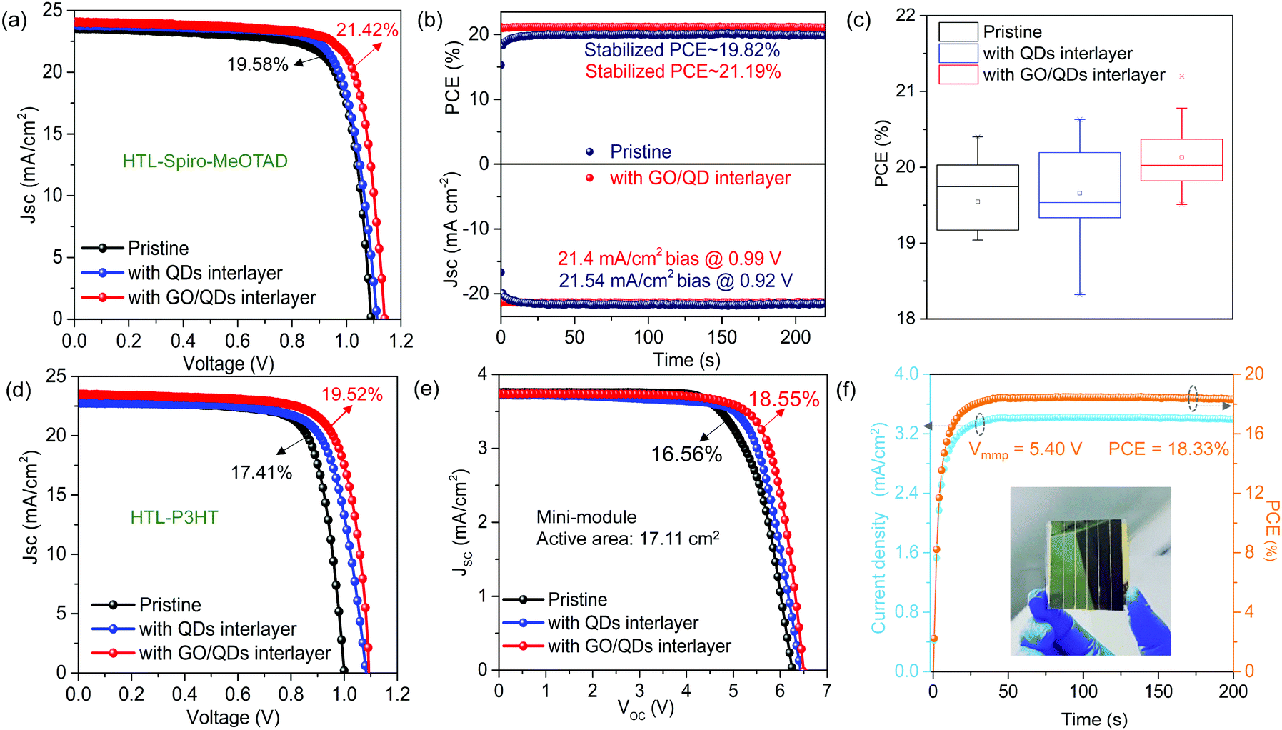
To evaluate the illumination stability of the perovskite film, the PL test was monitored at different times under continuous AM 1.5 G illumination. The fluorescence images were depicted in Fig. 5a and b. The results show that the GO/QDs composite inhibited the decomposition of perovskite films with less reduction in PL intensity over time. We also analyzed the depth profile of iodide ion (I−) and Au element within the cells by time-of-flight secondary ion mass spectroscopy (TOF-SIMS) (Fig. 5c and d).46 It was observed that I− demonstrated much higher signal intensities in the HTL layer and Au electrode of pristine cells than that of the PSC device with the GO/QDs interlayer. In addition, the mapping of I− inside the HTL shows a negligible signal in PSC with GO/QDs (Fig. 5e and f), which is in agreement with the depth profile analysis. These results obviously demonstrate that the crosslinked GO/QDs interlayer is an effective barrier against I− migration, which is favorable to protect the Au electrode from iodide erosion.47–49
 | ||
| Fig. 5 Time-dependent PL spectra of perovskite films under continuous simulated AM 1.5 G illumination for 2 weeks: (a) pristine, and (b) with the GO/QDs interlayer. TOF-SIMS depth profiles of iodide ion, Au, and Pb distribution in PSCs: (c) pristine, and (d) with the GO/QDs interlayer. Mapping of I− signals in the HTL within different devices: (e) pristine, and (f) with the GO/QDs interlayer. Spiro-MeOTAD was used as the HTL. All samples were aged under light-soaking for 1000 hours at the maximum power point. | ||
The GO/QDs interlayer is also an effective barrier against moisture. Moisture stability in extreme conditions showed that the color of pristine perovskite changed from black to yellow immediately after dropping water on the film. The perovskite film with the GO/QDs interlayer survived for a longer time (Fig. S13, ESI†). XRD spectra of fresh and thermal aged perovskite film, perovskite with QDs, and perovskite with GO/QDs in the air (20% relative humidity is shown in Fig. 6a and b). After a period of thermal treatment, all samples decomposed due to the volatile composition loss of the A-site cation, inducing the conversion of perovskite to PbI2. The film with GO/QDs showed the slowest decomposition rate among the three samples. To characterize the dominant A-site cation of the perovskite component (i.e., FA+; MA+ is below the detection level) distribution in aged perovskite films at 100 °C for 300 h in air, AFM-based infrared spectroscopy (AFM-IR) was performed.50Fig. 6c and d present the AFM topography for intentionally aged perovskite films. From the IR broadband map, we observe pronounced homogeneity in the perovskite film with the GO/QD interlayer, compared to the perovskite film without interlayer. A lower concentration of FA+ cations in grain boundaries was observed in the perovskite film without an interlayer, which is in line with that the strongest decomposition intensity of the FA cation (Fig. 6e and f). XRD tests further verified the perfect preservation of perovskite films in the humid and thermal environment with the GO/QDs interlayer (Fig. S14, ESI†).
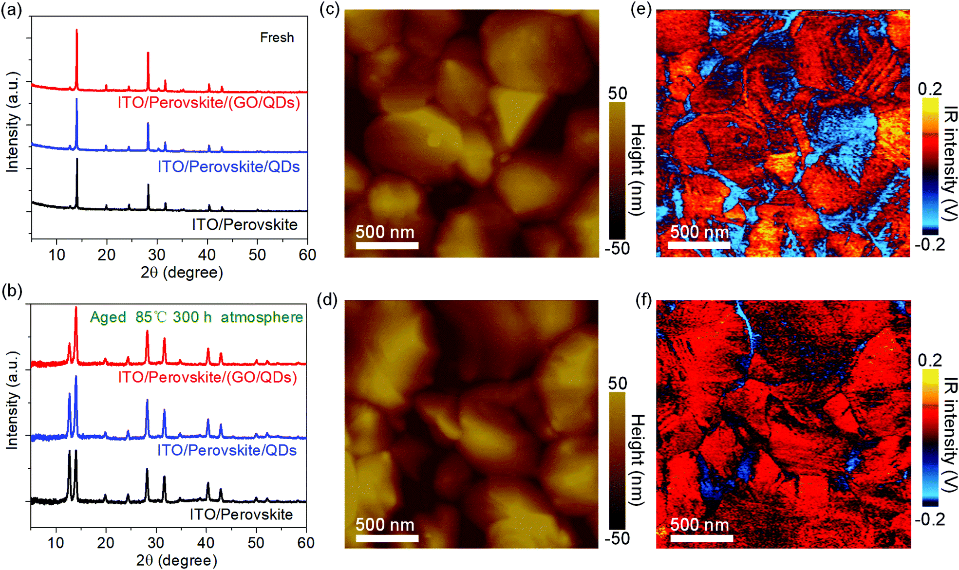 | ||
| Fig. 6 XRD spectra of (a) fresh and (b) aged perovskite films at 85 °C for 300 h. AFM images of aged perovskite films: (c) pristine, and (d) with the GO/QDs interlayer. IR for FA+ spatial distribution obtained from aged perovskite films: (e) pristine, and (f) with the GO/QDs interlayer. All samples were aged for 300 hours at 100 °C in air. | ||
We monitored the long-term thermal stability of the encapsulated module at 85 °C with 60% relative humidity (Fig. 7a). Fig. S15 (ESI†) shows the illustrations of the encapsulation process of PSMS. The module with the GO/QDs interlayer exhibited excellent thermal stability, with the PCE maintaining 91% of its initial PCE for 1000 h. However, the module with the QD interlayer maintained 60% of its initial efficiency, and the pristine device was almost destroyed. On one hand, the perovskite film containing the GO/QDs interlayer has enhanced hydrophobicity as compared to either the pristine or QD-containing sample, which indicates increased humidity resistance, and, accordingly, improved device stability with GO/QDs under moisture. On the other hand, the degradation of perovskite films was generally initialized at the surface defects.51 Crosslinking GO/QDs effectively passivate surface defects of the perovskite film, and, consequently, suppress the defect-induced decomposition. Thus, the outstanding thermal and humidity stability is ascribed to the collective effects of suppressing moisture penetration and passivating surface defects exerted by the GO/QD interface modulator.
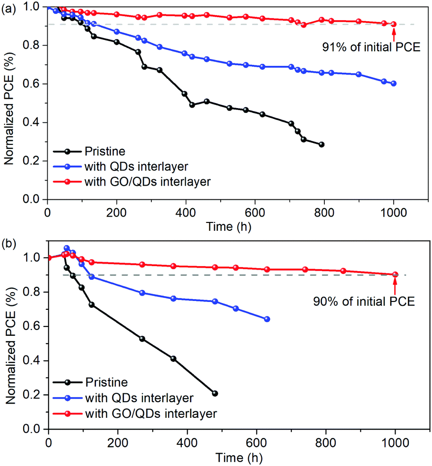 | ||
| Fig. 7 Operational stability of PSMs for the encapsulated devices. (a) Thermal stability at 85 °C and relative humidity of about 60%. (b) Light stability under continuous simulated AM 1.5 light illumination at 60 °C in ambient air. | ||
In addition, the PCE of both the pristine and QDs-containing PSMs degraded seriously after aging under continuous 1-sun illumination at the maximum power point over 1000 h, while in stark contrast, the module with the GO/QDs interlayer exhibited excellent stability during the same operation conditions, with the PCE maintaining 90% of its initial efficiency of over 18% (Fig. 7b and Table S4, ESI†), suggesting that the GO segment rather than the CsPbX3 QD component in the GO/QD interlayer exerts a key role in long-term stability enhancement. This is the most stable perovskite mini-module of the n–i–p structure reported so far with an initial active area efficiency of over 18%.20,53 Under illumination, the light-induced potential causes ion migration leading to degradation.52 The GO/QD interlayer in PSCs, as a barrier layer, would effectively suppress the ion migration, which is favorable to protect the Au electrode from iodide erosion, and, accordingly, favoring the stability of PSMs.
The high performance and stable PSC modules with the GO/QD interlayer were related to the following factors: (1) the suppression of ion migration, maintaining good capability of the HTL and electrode; (2) significantly passivated traps and suppressed carrier recombination; (3) high electrical conductivity and well-matched energy bands to promote carrier transport. The outstanding efficiency and stability of the PSM confirmed extraordinary potential toward commercialization.
Conclusions
In summary, we demonstrated a crosslinking strategy by introducing a scalable and multifunctional GO/QD interlayer modulator to lower resistive losses, through effectively improved carrier management while dramatically inhibiting ion/molecule diffusion within the solar cell, thus synergistically boosting the photovoltaic performance and stability of PSMs. Specifically, the GO/QD interlayer with improved conductivity and better-matched energy-level alignment to HTL boost carrier transport across the perovskite/HTL interface, decreasing the series resistance. Simultaneously, the GO/QD interlayer passivates the surface defects of perovskite to reduce carrier recombination losses, increasing the shunt resistance. Finally, by employing the crosslinked GO/QD interlayer, the PSMs by the VASP method achieved a certified steady-state efficiency of 17.85% on a 6 × 6 cm2 substrate, which was among the highest efficiencies reported for certified mini-PSMs. Our work demonstrates the important interaction among carrier management, interfacial recombination, and ion/molecule diffusion regulation, which is essential to improve the performance and stability of PSMs. This interface modulating strategy based on the scalable low-temperature solution-process method augments no complexity to fabrication, thus being applicable for commercial manufacturing of low-cost, high-efficiency, and stable PSMs.Author contributions
S. Zhang and R. Guo designed and wrote the outline of the review manuscript. S. Zhang designed the experiment. H. Zeng and Y. Zhao helped to synthesize materials. L. Long, M. Li, L, Li, S. You, and S. Zhang prepared and characterized the devices. X. Li supervised the overall project. All authors analyzed the results.Conflicts of interest
There are no conflicts to declare.Acknowledgements
The authors acknowledge financial from the National Natural Science Foundation of China (21875081, 91733301, and 51972251), the Chinese National 1000-Talent-Plan program, the Foundation of State Key Laboratory of Coal Conversion (Grant No. J18-19-913), and the Frontier Project of the Application Foundation of Wuhan Science and Technology Plan Project (2020010601012202). The authors thank Suzhou Vacuum Interconnected Nanotech Workstation (NANO-X) for providing the beam time. The authors thank the Analytical and Testing Center of Huazhong University of Science and Technology at Wuhan Photoelectric National Research Center (WNLO) for performing various characterizations and measurements.References
- N.-G. Park and K. Zhu, Nat. Rev. Mater., 2020, 5, 333–350 CrossRef CAS.
- G. Tong, D.-Y. Son, L. K. Ono, Y. Liu, Y. Hu, H. Zhang, A. Jamshaid, L. Qiu, Z. Liu and Y. Qi, Nat. Commun., 2021, 11, 2003712 CAS.
- S. K. Hau, H.-L. Yip, O. Acton, N. S. Baek, H. Ma and A. K. Y. Jen, J. Mater. Chem., 2008, 18, 5113–5119 RSC.
- C.-J. Ko, Y.-K. Lin, F.-C. Chen and C.-W. Chu, J. Mater. Chem., 2007, 90, 063509 Search PubMed.
- X. Li, D. Bi, C. Yi, J.-D. Décoppet, J. Luo, S. M. Zakeeruddin, A. Hagfeldt and M. Grätzel, Science, 2016, 353, 58–62 CrossRef CAS.
- D.-N. Jeong, D.-K. Lee, S. Seo, S. Y. Lim, Y. Zhang, H. Shin, H. Cheong and N.-G. Park, ACS Energy Lett., 2019, 4, 1189–1195 CrossRef CAS.
- Y. Deng, E. Peng, Y. Shao, Z. Xiao, Q. Dong and J. Huang, Energy Environ. Sci., 2015, 8, 1544–1550 RSC.
- T. Bu, J. Li, F. Zheng, W. Chen, X. Wen, Z. Ku, Y. Peng, J. Zhong, Y.-B. Cheng and F. Huang, Nat. Commun., 2018, 9, 4609 CrossRef PubMed.
- Y. Hu, S. Si, A. Mei, Y. Rong, H. Liu, X. Li and H. Han, Sol. RRL, 2017, 1, 1600019 CrossRef.
- P.-S. Shen, J.-S. Chen, Y.-H. Chiang, M.-H. Li, T.-F. Guo and P. Chen, Adv. Mater. Interfaces, 2016, 3, 1500849 CrossRef.
- D.-K. Lee, D.-N. Jeong, T. K. Ahn and N.-G. Park, ACS Energy Lett., 2019, 4, 2393–2401 CrossRef CAS.
- J. Kim, J. S. Yun, Y. Cho, D. S. Lee, B. Wilkinson, A. M. Soufiani, X. Deng, J. Zheng, A. Shi, S. Lim, S. Chen, Z. Hameiri, M. Zhang, C. F. J. Lau, S. Huang, M. A. Green and A. W. Y. Ho-Baillie, ACS Energy Lett., 2017, 2, 1978–1984 CrossRef CAS.
- X. Dai, Y. Deng, C. H. Van Brackle, S. Chen, P. N. Rudd, X. Xiao, Y. Lin, B. Chen and J. Huang, Adv. Energy Mater., 2020, 10, 1903108 CrossRef CAS.
- Z. Xu, R. Chen, Y. Wu, R. He, J. Yin, W. Lin, B. Wu, J. Li and N. Zheng, J. Mater. Chem. A, 2019, 7, 26849–26857 RSC.
- R. Chen, Y. Wu, Y. Wang, R. Xu, R. He, Y. Fan, X. Huang, J. Yin, B. Wu, J. Li and N. Zheng, Adv. Funct. Mater., 2021, 31, 2008760 CrossRef CAS.
- H. Chen, F. Ye, W. Tang, J. He, M. Yin, Y. Wang, F. Xie, E. Bi, X. Yang, M. Grätzel and L. Han, Nature, 2017, 550, 92–95 CrossRef CAS PubMed.
- Y. Deng, X. Zheng, Y. Bai, Q. Wang, J. Zhao and J. Huang, Nat. Energy, 2018, 3, 560–566 CrossRef CAS.
- Z. Yang, W. Zhang, S. Wu, H. Zhu, Z. Liu, Z. Liu, Z. Jiang, R. Chen, J. Zhou, Q. Lu, Z. Xiao, L. Shi, H. Chen, L. K. Ono, S. Zhang, Y. Zhang, Y. Qi, L. Han and W. Chen, Sci. Adv., 2021, 7, eabg3749 CrossRef CAS PubMed.
- Y. Deng, S. Xu, S. Chen, X. Xiao, J. Zhao and J. Huang, Nat. Energy, 2021, 6, 633–641 CrossRef CAS.
- Y. Sha, E. Bi, Y. Zhang, P. Ru, W. Kong, P. Zhang, X. Yang, H. Chen and L. Han, Adv. Energy Mater., 2021, 11, 2003301 CrossRef CAS.
- A. Ren, H. Lai, X. Hao, Z. Tang, H. Xu, B. M. F. Yu Jeco, K. Watanabe, L. Wu, J. Zhang, M. Sugiyama, J. Wu and D. Zhao, Joule, 2020, 4, 1263–1277 CrossRef CAS.
- C. C. Boyd, R. Cheacharoen, T. Leijtens and M. D. McGehee, Chem. Rev., 2019, 119, 3418–3451 CrossRef CAS PubMed.
- M. Yang, D. H. Kim, T. R. Klein, Z. Li, M. O. Reese, B. J. Tremolet de Villers, J. J. Berry, M. F. A. M. van Hest and K. Zhu, ACS Energy Lett., 2018, 3, 322–328 CrossRef CAS.
- E. Bi, W. Tang, H. Chen, Y. Wang, J. Barbaud, T. Wu, W. Kong, P. Tu, H. Zhu, X. Zeng, J. He, S.-i. Kan, X. Yang, M. Grätzel and L. Han, Joule, 2019, 3, 2748–2760 CrossRef CAS.
- Z. Liu, L. Qiu, L. K. Ono, S. He, Z. Hu, M. Jiang, G. Tong, Z. Wu, Y. Jiang, D.-Y. Son, Y. Dang, S. Kazaoui and Y. Qi, Nat. Energy, 2020, 5, 596–604 CrossRef CAS.
- F. Cheng, R. He, S. Nie, C. Zhang, J. Yin, J. Li, N. Zheng and B. Wu, J. Am. Chem. Soc., 2021, 143, 5855–5866 CrossRef CAS PubMed.
- H. Bian, D. Bai, Z. Jin, K. Wang, L. Liang, H. Wang, J. Zhang, Q. Wang and S. Liu, Joule, 2018, 2, 1500–1510 CrossRef CAS.
- X.-X. Feng, X.-D. Lv, Q. Liang, J. Cao and Y. Tang, Appl. Mater. Interfaces, 2020, 12, 16236–16242 CrossRef CAS PubMed.
- M. Hadadian, J.-H. Smått and J.-P. Correa-Baena, Energy Environ. Sci., 2020, 13, 1377–1407 RSC.
- L. Protesescu, S. Yakunin, M. I. Bodnarchuk, F. Krieg, R. Caputo, C. H. Hendon, R. X. Yang, A. Walsh and M. V. Kovalenko, Nano Lett., 2015, 15, 3692–3696 CrossRef CAS PubMed.
- Y. Zhang, X. Liu, P. Li, Y. Duan, X. Hu, F. Li and Y. Song, Nano Energy, 2019, 56, 733–740 CrossRef CAS.
- J. Tian, Q. Xue, X. Tang, Y. Chen, N. Li, Z. Hu, T. Shi, X. Wang, F. Huang, C. J. Brabec, H.-L. Yip and Y. Cao, Adv. Mater., 2019, 31, 1901152 CrossRef PubMed.
- T. Singh and T. Miyasaka, Adv. Energy Mater., 2018, 8, 1700677 CrossRef.
- S. You, H. Zeng, Z. Ku, X. Wang, Z. Wang, Y. Rong, Y. Zhao, X. Zheng, L. Luo, L. Li, S. Zhang, M. Li, X. Gao and X. Li, Adv. Mater., 2020, 32, 2003990 CrossRef CAS PubMed.
- O. Almora, C. Aranda, E. Mas-Marzá and G. Garcia-Belmonte, Appl. Phys. Lett., 2016, 109, 173903 CrossRef.
- S. Ye, H. Rao, Z. Zhao, L. Zhang, H. Bao, W. Sun, Y. Li, F. Gu, J. Wang, Z. Liu, Z. Bian and C. Huang, J. Am. Chem. Soc., 2017, 139, 7504–7512 CrossRef CAS.
- C. Ran, J. Xu, W. Gao, C. Huang and S. Dou, Chem. Soc. Rev., 2018, 47, 4581–4610 RSC.
- Y. Shao, Z. Xiao, C. Bi, Y. Yuan and J. Huang, Nat. Commun., 2014, 5, 5784 CrossRef CAS.
- G. Balaji, H. A. Abbas and P. J. A. P. L. Joshi, Appl. Phys. Lett., 2014, 105, 153502 CrossRef.
- G. Tang, P. You, Q. Tai, R. Wu and F. Yan, Sol. RRL, 2018, 2, 1800066 CrossRef.
- M. A. Lampert, Phys. Rev., 1956, 103, 1648 CrossRef CAS.
- J. Sworakowski and K. Pigoń, J. Phys. Chem. Solids, 1969, 30, 491–496 CrossRef CAS.
- J. Chen and N.-G. Park, Adv. Mater., 2019, 31, 1803019 CrossRef CAS PubMed.
- D. Yang, R. Yang, K. Wang, C. Wu, X. Zhu, J. Feng, X. Ren, G. Fang, S. Priya and S. Liu, Nat. Commun., 2018, 9, 3239 CrossRef PubMed.
- S. You, H. Wang, S. Bi, J. Zhou, L. Qin, X. Qiu, Z. Zhao, Y. Xu, Y. Zhang, X. Shi, H. Zhou and Z. Tang, Adv. Mater., 2018, 30, 1706924 CrossRef PubMed.
- S. Hong, J. Lee, H. Kang, G. Kim, S. Kee, J.-H. Lee, S. Jung, B. Park, S. Kim, H. Back, K. Yu and K. Lee, Sci. Adv., 2018, 4, eaat3604 CrossRef CAS PubMed.
- J. Chen, D. Lee and N.-G. Park, ACS Appl. Mater. Interfaces, 2017, 9, 36338–36349 CrossRef CAS PubMed.
- D. W. deQuilettes, W. Zhang, V. M. Burlakov, D. J. Graham, T. Leijtens, A. Osherov, V. Bulović, H. J. Snaith, D. S. Ginger and S. D. Stranks, Nat. Commun., 2016, 7, 11683 CrossRef CAS PubMed.
- C. Eames, J. M. Frost, P. R. F. Barnes, B. C. O’Regan, A. Walsh and M. S. Islam, Nat. Commun., 2015, 6, 7497 CrossRef CAS PubMed.
- R. Szostak, J. C. Silva, S.-H. Turren-Cruz, M. M. Soares, R. O. Freitas, A. Hagfeldt, H. C. N. Tolentino and A. F. Nogueira, Sci. Adv., 2019, 5, eaaw6619 CrossRef CAS PubMed.
- E. J. Juarez-Perez, L. K. Ono and Y. Qi, J. Mater. Chem. A, 2019, 7, 16912–16919 RSC.
- Y. Yuan and J. Huang, Acc. Chem. Res., 2016, 49, 286–293 CrossRef CAS PubMed.
- T. Bu, J. Li, H. Li, C. Tian, J. Su, G. Tong, L. K. Ono, C. Wang, Z. Lin, N. Chai, X.-L. Zhang, J. Chang, J. Lu, J. Zhong, W. Huang, Y. Qi, Y.-B. Cheng and F. Huang, Science, 2021, 372, 1327–1332 CrossRef CAS PubMed.
Footnotes |
| † Electronic supplementary information (ESI) available. See DOI: 10.1039/d1ee01778k |
| ‡ These authors contributed equally to this work. |
| This journal is © The Royal Society of Chemistry 2022 |