
 Open Access Article
 This Open Access Article is licensed under a
 Creative Commons Attribution 3.0 Unported Licence
Accelerated automated screening of viscous graphene suspensions with various surfactants for optimal electrical conductivity
Daniil
Bash
 ab,
Frederick Hubert
Chenardy
c,
Zekun
Ren
d,
Jayce J
Cheng
b,
Tonio
Buonassisi
de,
Ricardo
Oliveira
f,
Jatin N
Kumar
b and
Kedar
Hippalgaonkar
*bc
ab,
Frederick Hubert
Chenardy
c,
Zekun
Ren
d,
Jayce J
Cheng
b,
Tonio
Buonassisi
de,
Ricardo
Oliveira
f,
Jatin N
Kumar
b and
Kedar
Hippalgaonkar
*bc
aDepartment of Chemistry, National University of Singapore, 3 Science Drive, Singapore, 117543, Singapore
bInstitute of Materials Research and Engineering, Agency for Science, Technology and Research (A*STAR), #08-03, 2 Fusionopolis Way, Innovis, Singapore, 138634, Singapore
cDepartment of Materials Science and Engineering, Nanyang Technological University, 50 Nanyang Ave, Block N4.1, Singapore, 639798, Singapore. E-mail: kedar@ntu.edu.sg
dSingapore-MIT Alliance for Research and Technology, 1 Create Way, #10-01 & #09-03 CREATE Tower, Singapore, 138602, Singapore
eDepartment of Mechanical Engineering, Massachusetts Institute of Technology, Cambridge, Massachusetts 02139, USA
f2D Materials Pte Ltd (2DM), Singapore
First published on 27th January 2022
Abstract
Functional composite thin films have a wide variety of applications in flexible and/or electronic devices, telecommunications and multifunctional emerging coatings. The rapid screening of their properties is a challenging task, especially with multiple components defining the targeted properties. In this work we present a platform for accelerated automated screening of viscous graphene suspensions for optimal electrical conductivity. Using an Opentrons OT2 robotic auto-pipettor, we tested 3 most industrially significant surfactants – PVP, SDS and T80 – by fabricating 288 samples of graphene suspensions in aqueous hydroxypropylmethylcellulose. Enabled by our custom motorized 4-point probe measurement setup and computer vision algorithms, we then measured the electrical conductivity of every sample and identified that the highest performance is achieved for PVP-based samples, peaking at 10.8 mS cm−1 without annealing. The automation of the experimental procedure allowed us to perform the majority of the experiments using robots, while the involvement of human researchers was kept to minimum. Overall the experiment was completed in less than 18 hours, only 3 of which involved humans.
Introduction
In recent years, printable flexible electronics have received increasing attention.1–5 Specifically, conductive inks and paints have attracted much attention, as these materials show a wide range of applications, for example, printed radio frequency identification devices (RFIDs),6 surface heaters,7 wearable printable sensors,8,9 IoT devices,10 conductive fabrics,11,12etc. One of the most explored additive for manufacturing conductive inks and paints is graphene10,12–18 due to its intrinsic high electrical and thermal conductivity,19–21 chemical and thermal stability,22–25 and a relatively low price. However, because it is so chemically inert, graphene faces challenges when being made into dispersions, as it has very low affinity to most solvents, and, therefore, tends to aggregate and precipitate from the solution.A common way to overcome this challenge is the use of surfactants.4,12 Surfactants help to separate graphene flakes from each other and prevent their aggregating, while also significantly increasing their affinity to the solvent.26,27 However, excessive quantities of surfactant drastically reduce the electrical conductivity of the resulting device since individual graphene flakes are shielded by surfactant molecules and cannot form an efficient path for charge carriers to flow through.28 Hence, finding an optimal type and concentration of the surfactant is a key challenge for industry as these properties have a critical impact on the performance of the final device, bill of materials (BOM), and overall cost of manufacturing. Several studies have been carried out to identify the best surfactants for graphene dispersion in various solvents.26,28–31
Surfactants like sodium dodecylsulphate (SDS), polyvinylpyrrolidone (PVP) and tween 80 (T80), among several others, have been shown to have the most optimal properties for graphene dispersion.32–35 Industrially, the optimization of graphene–surfactant formulation is of major importance as described above. To our knowledge, very few studies have explored the parameter space of graphene–surfactant mixtures in full or performed detailed characterization of the conductivity profiles of the samples. This can partially be explained by the fact that traditional manual methods of sample preparation are inadequate for covering a large parameter space. Therefore, we thought it necessary to develop a robust high-throughput method for the automation of liquid sample preparation, drop-casting and thin film characterization. The use of robotics and automation allows for highly reproducible, systematic fabrication of hundreds and thousands of samples with almost no human intervention.
In this work, we develop a methodology for the fabrication of graphene–surfactant mixtures of various ratios in an automated fashion, thin film preparation and accelerated characterization. To achieve that, we used an Opentrons OT2 auto-pipettor (Fig. 1a) to perform an exhaustive search of the full parameter space for ternary mixtures of graphene, hydroxypropylmethylcellulose (HPMC) and each of the 3 surfactants: PVP, SDS and T80. We used custom python-based software to generate the design of experiment (DoE) in csv format, which was used to provide instructions for the auto-pipettor for mixing and drop-casting.
 | ||
| Fig. 1 Schematic representation of the experimental workflow and distribution of time spent by humans and by robots. (a) Fabrication of samples using an Opentrons OT2 auto-pipettor (image credit: Opentrons); (b) image of drop-cast samples; (c) automated 4-point probe measurement setup; (d) samples labelled by the computer-vision algorithm. Time estimations are provided per 96 samples, or one surfactant. | ||
An advantage of our approach is the robustness of the system for a varied range of viscous solutions. Specifically, we used HPMC, a common rheology modifier, to mimic the viscosity and the film-formation characteristics of an ink/paint.36 Despite the added complexity of our control software, the auto-pipettor was able to handle viscous liquids without affecting the quality of the samples or the reproducibility of the experiment. Importantly, we significantly improved the efficiency and the throughput for the fabrication of the samples, which was less than 2 minutes per sample, including mixing of the stock solution to obtain the desired graphene–surfactant ratio, and subsequent drop-casting, or approximately a 2-5-fold increase of the throughput compared to the manual process (Fig. 1). The involvement of human researchers was limited to loading samples in and out of the autopipettor and checking the calibration during the fabrication stage and to positioning the 4pp tool above samples and post-processing the image recognition data during the measurement stage.
The rapid fabrication of test samples without a robust methodology for high-throughput characterization of these samples would have little benefit, especially for the use of supervised learning algorithms. Therefore, we have developed automated characterization techniques, which involve a 4-point probe (4pp) for automated full IV measurement, as well as a computer vision-based algorithm for thickness approximation (Fig. 1c and d respectively). The automation of the 4pp measurement has an added advantage of causing minimal damage to the samples and is highly reproducible due to the computer vision-based indexing of the samples' positions.
Traditionally, in manual measurements the probe is pressed into the sample by hand and is held there by the researcher until the measurement is done, which takes a few minutes, in addition to positioning and setting up the instrument. However, it is almost impossible to hold the probe at exactly the same angle and at constant force during this procedure. Hence, the samples could be damaged by probe slipping, and the results of measurement might not be consistent. In contrast, the automated manipulation of the probe allows us to always apply uniform pressure and at exactly the right angle, minimizing the damage to the sample and yielding highly reproducible results, while freeing up the hands and mind of the researcher. Some of the automated 4pp measurements involve the use of refurbished 3D-printers with all open-source components, described by Handy Chandra et al.;37 the use of micro electro-mechanical system (MEMS) based micro- or nano-4pp for in situ measurements of large material libraries, developed by Alfred Ludwig et al.;38 the use of an automated 4pp stage for measuring the Hall effect, as described in work by Rudolf Kinder et al.,39 among others.
In contrast, the advantages of our method of 4pp measurements include the use of off-the-shelf components, which are commonly in possession of research groups that are involved in thin film fabrication and characterization, and only minimal requirement of coding or electrical engineering skills, as compared to the majority of alternative approaches from the literature. Our approach, on par with complementary techniques, allowed us to increase the throughput to approximately 1 minute per sample, where a full wafer with 49 samples is automatically characterized in ∼45 minutes including detection, alignment and measurement, which is 3–5 times faster than manual measurements (Fig. 1c). The obtained IV curves were then converted into sheet resistance and were used for further processing in this study.
The next automation step of our methodology is the computer vision-based thickness approximation algorithm. It was used for detecting the exact outline of the sample for calculating its area in pixels, which was then correlated with the true area of reference samples – 2 black circles with a known area printed on A4 paper, placed underneath the wafer (Fig. 1b and d, bottom right corner). Thereafter, we were able to calculate the thickness of the samples, based on known dispensed volume and concentration for every sample. These thickness data, combined with sheet resistance data, were used to calculate the property of interest – electrical conductivity. Overall, the full workflow, including the fabrication and full characterization of all 288 samples, was completed in ∼18 hours spread across 3 days, out of which ∼15 hours were fully automated, thus taking a focused human time of only 3 hours. It is worth mentioning that the majority of the fabrication time was spent on programmed 3 seconds delays to let the viscous HPMC to flow in and out of the pipette tip. When applied to non-viscous solutions, the same protocol is completed within10 minutes, compared to 3.5 hours for viscous ones.
This ability to perform experiments rapidly allows the use of dispersions that are stable over a period of only a few hours, which enables the researchers to broaden the parameter space and go beyond the compositions of infinitely stable dispersions. This opens a plethora of opportunities to explore large parameter spaces of increasing complexity in a high-throughput manner, enabled by a combination of automated mixing, drop-casting, and testing systems.
Methods
The parameter space of graphene-to-surfactant ratios in HPMC was sampled uniformly with 2% increments with 8 to 18% surfactant for PVP and T80 samples, and 2 to 12% surfactant for SDS, where graphene was varied from 0 to 30% also with 2% increments, with the solution of HPMC filling the remaining part of the composition. The higher initial ratio of surfactant for PVP and T80 was dictated by the limitations of the stability of the stock solution of the graphene, while dispersions with SDS were comparatively stable at lower ratios of surfactant. The stock solutions of graphene were prepared by probe sonication for 3 hours of a mixture of graphene and surfactant at the highest graphene-to-surfactant ratio used for the given surfactant, so that the total concentration of solids was kept constant at 1 mg ml−1. The stock solutions of HPMC and surfactants were prepared by simply mixing with deionized water at 1 mg ml−1 concentration and overnight stirring. As our experiment was not limited by the throughput neither in experiments not in metrology, we had no need to deploy an “intelligent agent” to select the next set of parameters, since the full parameter space was accessible to us through full-factorial design of experiments.Experimental setup
The main tool used for the fabrication of the samples in this work was an Opentrons OT2 auto-pipettor. Controlled by an onboard Raspberry Pi, it received instructions in the form of a .CSV file with volumes and positions for all operations. The robot then automatically distributed required amounts of ingredients into the corresponding wells of a 96-well plate, using a new tip for each solution. After distribution, the robot was programmed to repeatedly aspirate and dispense the mixture in each well 10 times with varying heights to ensure proper mixing and then drop-cast the resulting mixture onto a pre-treated fused silica wafer. The tip was washed by 5 repeated aspirations and dispensing of water each in 3 consecutive vials before moving to the next sample.While working with the HPMC solution, to account for its high viscosity, the robot was programmed to take a 3 seconds pause after every aspiration and dispensing operation, to allow the pressure in the pipette tip to stabilize. Another necessary added process step was the dipping of the pipette tip into the HPMC solution to a depth of <2 mm from the meniscus, to minimize the HPMC's adhesion to the outer walls of the pipette and prevent interference with the determined dispense volume.
Analytical setup
After deposition and drying, the samples were tested for their electrical conductivity using a custom automated 4-point probe measurement setup. The setup is equipped with a computer-controlled XY-stage, the probe itself, which is connected to a Keithley 2450, and an optical camera. Prior to measurements, the camera takes a picture of the wafer with samples, to run an image recognition algorithm. This algorithm detects the exact contour of every sample, calculating its area in pixels and coordinates of the center of mass, which is then used to index the positions for the electrical measurements, as seen in Fig. 1d. For each sample, we obtained a current–voltage (I–V) curve, slope of which was then used to calculate the sheet resistance. All measurements were done in a 4-point probe configuration, to ensure maximum quality of the data and a linear slope. After the sheet resistance was recorded, we calculated the true area of each sample by relating the measured area in pixels to an area of 2 reference samples of known sizes (eqn (1) and (2)). Here A is the area of the sample and k is a calibration coefficient| Atrue = kApixel | (1) |
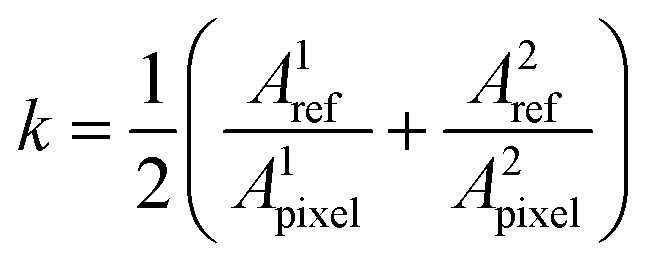 | (2) |
The obtained coefficients were averaged and applied to the rest of the samples on the wafer to obtain the value of the true area. Then, combining it with a known dispensed volume of each sample, we calculated the thickness of the samples. To make this link a few key assumptions are made: (1) the volume of the drop-cast samples is identical for all samples, down to the technical limitations of the Opentrons; (2) every sample has an identical total concentration of solids, down to the technical limitations of analytical balances and neglecting minute errors during the transference of solutions; (3) the surfaces of the samples are flat and uniform, acknowledging that this assumption is the biggest source of error, but still accurate enough to be used for screening purposes. It is worth mentioning that the calculated densities of all samples were found to be identical down to the second significant decimal point. We then compared our calculated thickness data to those of randomly selected 7% of samples, measured on a surface profiler. Note that the surface profilometry has its intrinsic errors, since it requires manual ‘scratching’ in the center of the sample and is by nature a single-line measurement, which is then extrapolated to the whole film. The mean absolute percentage error (MAPE) between the calculated thickness using the above assumption and measured thickness was found to be within 7–11% (Fig. 2), hence supporting the feasibility of this method for high-throughput screening of thickness for large quantities of electronic composites.
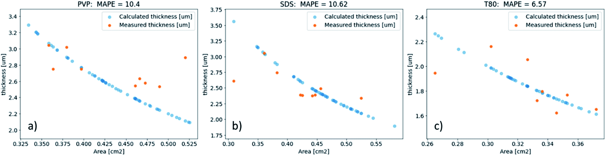 | ||
| Fig. 2 Comparison of the calculated thickness and that measured using profilometry. (a) for PVP-based samples, (b) for SDS-based samples, and (c) for T80-based samples. Each figure also shows the value of the Mean Absolute Percentage Error (MAPE). | ||
An integral component of the optical thickness measurement technique is the implementation of computer vision-based (OpenCV) algorithms. The OpenCV pipeline consists of a chain of algorithms including segmentation and contour detection as well as data processing of the individual sample area. A graphical user interface (GUI) was built in Python using the PySimpleGUI library, to allow flexible, real-time tuning of the key parameters, such as the segmentation threshold value, noise removal iterations, and distance transform mask size, to optimize the work of these algorithms.
Following the segmentation and detection of the films, each sample is index-labelled with an integer value, which is sorted from top-left to bottom-right. The contour features and moments of each film are then analyzed to produce the area data in pixels.
Based on the area pixel values, the thickness of a given film can be calculated by relating to the pixel values of 2 reference samples of known sizes (see eqn (1) and (2)). To quantify the error between the calculated thickness and thickness obtained from the surface profiler, we fit the calculated thickness to the area data and compute the MAPE for thickness values between the fitted sample and profilometry measured samples with different surfactants (PVP-based, SDS-based, and T80-based). As shown in Fig. 2, for all 3 cases, the MAPE is below 11%, which is acceptable for the high throughput proxy measurements. We use a Gaussian Process (GP) model to reproduce the equation that relates area to thickness values. The GP model is chosen as it can account for potential white noise errors that could arise from the computer vison algorithm and gives an uncertainty estimate. The GP kernel implemented here consists of a Radial Basis Function (RBF) kernel and a Whitenoise Kernel.
Results and discussion
The mechanism of conductivity in graphene-based composites is typically explained by percolation theory,40–43 according to which individual sheets of graphene form a connected network, allowing the flow of the charge carriers. However, when the concentration of graphene is low, below a percolation threshold, a fully connected network cannot be formed, and the charge carriers hop between the islands of graphene clusters via tunneling, which significantly decreases the conductivity of the composite.The results of our study show that films made using PVP as the surfactant are the most conductive, with the highest value of conductivity of 10.8 mS cm−1 (Fig. 3a), which is at least 2 orders of magnitude higher the current state of the art for similar material systems.44 Interestingly, the conductivity of PVP-based films does not show dependence on the concentration of PVP, unlike films made with other surfactants. SDS-based films show low conductivity values under most of the tested conditions, except for the samples with a high concentration of graphene, as seen in Fig. 3b. The concentration of SDS showed no significant influence on the device performance. The worst conductivity values were observed for films made using T80, where the highest observed conductivity was only 0.06 mS cm−1, as shown in Fig. 3c, which is about 3 orders of magnitude lower than that for PVP-based samples. The majority of the measured T80-based samples show conductivity values too low to be distinguished from instrument noise.
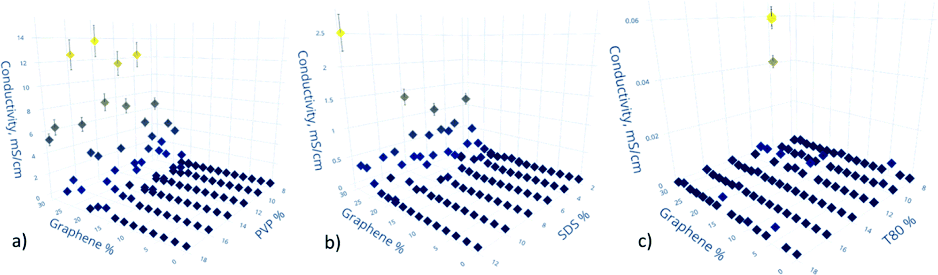 | ||
| Fig. 3 (a–c) Conductivity in mS cm−1vs. graphene ratio in % vs. surfactant ratio in %. Here, the percolation threshold is seen to be (a) ∼15% for PVP and (b) ∼20% for SDS, (c) while it is not reached for T80. The conductivity is highest for (a) PVP, followed by (b) SDS, while the (c) Graphene-T80 film doesn't conduct. | ||
We speculate that PVP shows the best results due to the higher affinity of its aromatic benzene rings to the aromatic rings of graphene, as compared to other surfactants used.45 Also, due to its polymer nature as compared to SDS, PVP could promote better alignment of graphene sheets and, therefore, increase the overall conductivity of the sample. SDS, on the other hand, despite showing mediocre conductivity results, could stabilize the dispersion at 4 times lower concentration compared to the other tested surfactants. This feature could be significant for specific industrial applications, e.g. high conductivity (10−1 to 102 S cm−1) for paint-on sensors or low conductivity (10−8–10−4 S cm−1) for anti-static coatings, as it could provide significant cost savings.
We explain the poor performance of the T80-based samples not by the inherit incompatibility of this surfactant as a stabilizing agent for graphene dispersions, but by excessively aggressive sonication parameters. The conditions used to sonicate the dispersions could have damaged the polymer chains to the point that the T80 lost most of its properties as a surfactant. The backbone of T80 is comprised of ester C–O bonds, which are weaker in nature, in contrast to C–C bonds in PVP. Future experiments will aim to investigate this assumption, by using a series of more mild sonicating conditions with T80-based composites.
Further analysis of the surface of the composites using Scanning Electron Micrographs (SEMs) revealed that the distribution of graphene inside the HPMC matrix is relatively uniform at the lowest surfactant load and highest and medium graphene loads (Fig. 4a–l respectively), suggesting the effectiveness of our dispersion and fabrication procedures. The scanning electron microscopy (SEM) images reveal that the graphene islands inside the composites are relatively dense; however, to test how much impact the separation of these islands by HPMC inside the composite has on the performance of the composites, we decided to anneal the samples beyond the decomposition temperature of HPMC and repeat the electrical measurements and SEM characterization.
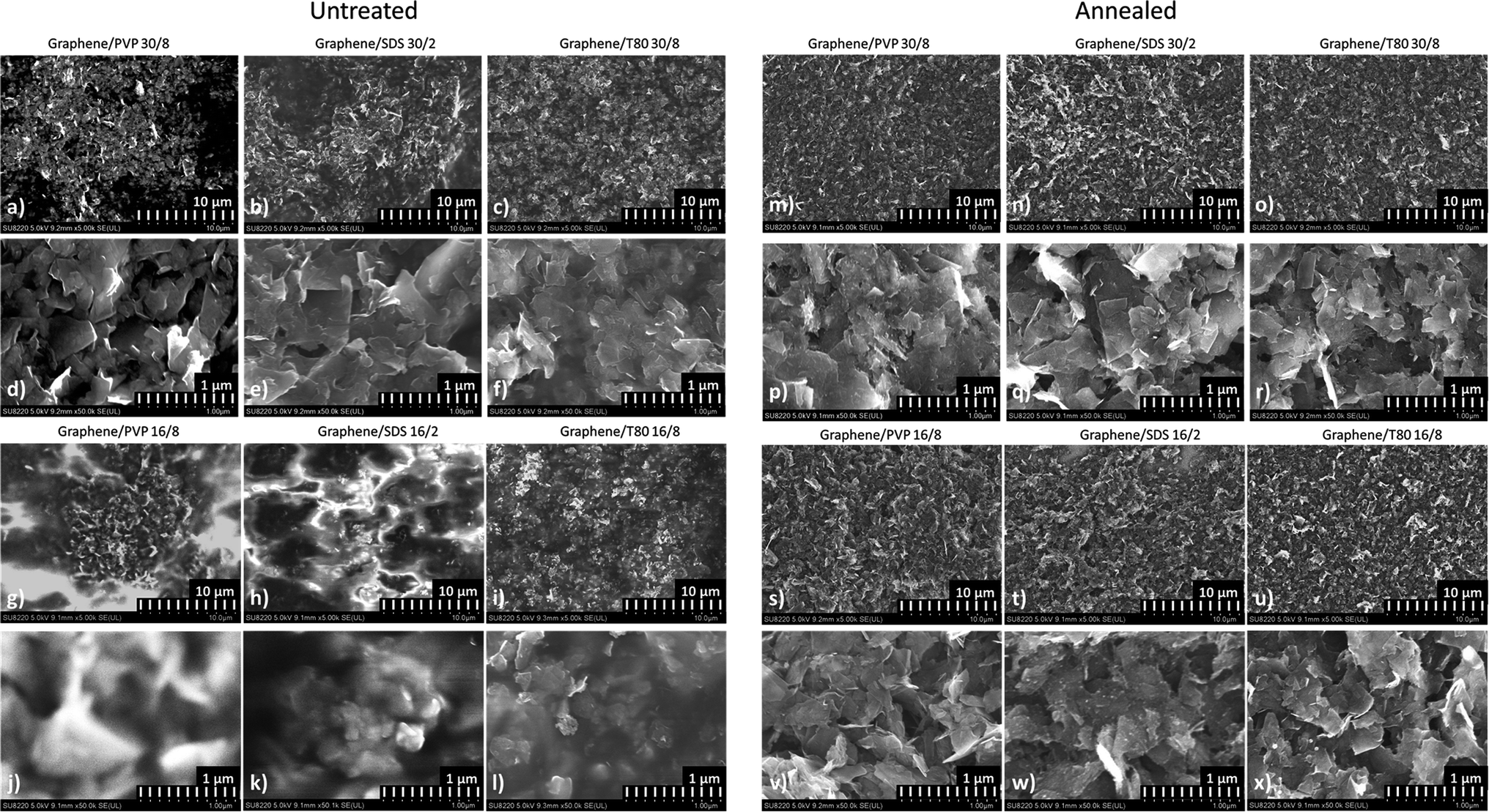 | ||
| Fig. 4 SEM images of selected samples: 5k magnification of high graphene load samples, (a–c) untreated (left), (m–o) annealed (right); 50k magnification of high graphene load samples, (d–f) untreated (left), (p–r) annealed (right); 5k magnification of medium graphene load samples, (g–i) untreated (left), (s–u) annealed (right); 50k magnification of medium graphene load samples, (j–l) untreated (left), (v–x) annealed (right). | ||
The same samples used for SEM imaging of samples without any post-processing were used to test the effect of annealing. The annealing was done in a vacuum furnace. First, the samples were brought from room temperature to 250 °C at 10 °C min−1, and then from 250 °C to 500 °C at 1 °C min−1 and held at 500 °C for 120 min to completely burn off the HPMC binder.
After annealing, the thickness and sheet resistance of the samples were measured again. We observed a conductivity increase up to 7 orders of magnitude, suggesting that with the removed polymer matrix, graphene flakes came into close contact with each other to form a dense percolation network. The highest increase in conductivity is observed for, expectedly, T80-based samples, because they were barely conductive prior to annealing, while for SDS-based samples the increase in conductivity is the lowest, most likely due to the lower influence of annealing on the stability of the surfactant molecule. As seen from the images in Fig. 4(m–x), the morphology of the annealed samples does not seem to depend on the surfactant, nor on the initial concentration of graphene inside the composite, as compared to untreated samples.
In principle, image analysis with computer vision algorithms can be performed on these SEM images to extract features that could be linked to electrical conductivity. However, a large number of images would have to been taken to provide a comprehensive dataset and hence we did not attempt this in the current manuscript. Although, one could envision undertaking such analysis in future work.
We also speculate that the introduction of simple automation into sonication and annealing processes could unlock another vast and sparsely sampled parameter space for studying the performance of composites that are made from dispersions. The slow and sequential nature of these steps was the main limiting factor for us not to try various sonication or annealing conditions. The community would greatly benefit from developments in automation protocols for these key processes.
Conclusions
In this work, we demonstrated a high-throughput methodology for automated mixing and drop-casting of graphene-based composites followed by their electrical conductivity measurement. We used a robotic auto-pipettor to explore more combinations of parameters (288 unique conditions tested) in 10× less time, as compared to traditional procedures, even using viscous liquids. The distribution of all ingredients, mixing and subsequent drop-casting of all samples were done within 12 hours, almost fully autonomously. In addition, when applied to electrical measurements, automation not only improves the throughput of the experiments, but also increases the reliability and reproducibility of the measurements, as every sample is precisely indexed and is measured with minimal damage to the film. We also show the utility of our method for rapid screening of thickness for thin-film samples, relying only on computer vision algorithms and the precision of the auto-pipettor to drop-cast exact volumes. Amongst all films prepared, the graphene dispersions made with PVP as the surfactant have the highest conductivity values as compared to samples made with SDS and T80, with the best result of 10.8 mS cm−1. We also identified that the relative concentration of the surfactant plays a minimal role in the overall performance of the composite, suggesting that the load of the graphene plays the most significant role.In conclusion, using this approach, we fabricated 288 samples in this study, with a goal to identify the best surfactant to be used for graphene dispersions, in less than a week of experimental work, most of which was done by robots. Hence, we demonstrate the viability and applicability of automation tools to scientific experiments, especially the ones which rely on many repetitive operations and exploration of vast parameter spaces. These techniques can free up most of the human workhours from the experiments, and delegate the tedious work to robots. Our work demonstrates the push towards automation in science laboratories, where human researchers are engaged in creative scientific work and planning of experiments, while execution is delegated to robots, machine learning algorithms and efficient high-throughput experimentation and analytical tools.
Data availability
The data and codes for the fabrication of samples and image processing can be found at https://github.com/Argarot/Accelerated-automated-screening-of-graphene-suspensions-with-surfactants-for-optimal-conductivityAuthor contributions
The author contributions are provided in CRediT format. D. Bash – conceptualization, investigation, methodology, formal analysis, software, validation, writing original draft, and visualization; F. H. Chenardi – software, writing original draft, and visualization; Z. Ren – formal analysis and visualization; J. Cheng – software and methodology; T. Buonassisi – conceptualization and project administration; R. Oliveira – conceptualization, resources, and writing review and editing; J. Kumar – conceptualization, project administration, and supervision; K. Hippalgaonkar – conceptualization, project administration, supervision, funding acquisition, resources, and writing review and editing.Conflicts of interest
The graphene sample for this study was provided by the company 2DM free of charge. Some of the authors own equity in companies applying machine learning to materials development.Acknowledgements
We'd like to thank Patrick Teyssoneyre for his effervescence and the members of the AMDM and Xinterra teams for discussions. J. J. C., J. N. K. and K. H. acknowledge funding from the Accelerated Materials Development for Manufacturing Program at A*STAR via the AME Programmatic Fund by the Agency for Science, Technology and Research under Grant No. A1898b0043. Z. R. and T. B. are supported by the National Research Foundation, Prime Minister’s Office, Singapore under its Campus for Research Excellence and Technological Enterprise (CREATE) program through the Singapore Massachusetts Institute of Technology (MIT) Alliance for Research and Technology’s Low Energy Electronic Systems (LEES) research program.Notes and references
- L. Grande, V. T. Chundi, D. Wei, C. Bower, P. Andrew and T. Ryhaenen, Particuology, 2012, 10, 1–8 CrossRef CAS.
- S. Ligati, A. Ohayon-Lavi, J. Keyes, G. Ziskind and O. Regev, Int. J. Therm. Sci., 2020, 153, 106381 CrossRef CAS.
- D. S. Saidina, N. Eawwiboonthanakit, M. Mariatti, S. Fontana and C. Hérold, J. Electron. Mater., 2019, 48, 3428–3450 CrossRef CAS.
- T. S. Tran, N. K. Dutta and N. R. Choudhury, Adv. Colloid Interface Sci., 2018, 261, 41–61 CrossRef CAS PubMed.
- M. H. Overgaard, M. Kühnel, R. Hvidsten, S. V. Petersen, T. Vosch, K. Nørgaard and B. W. Laursen, Adv. Mater. Technol., 2017, 2, 1700011 CrossRef.
- T. Leng, X. Huang, K. Chang, J. Chen, M. A. Abdalla and Z. Hu, IEEE Antenn. Wireless Propag. Lett., 2016, 15, 1565–1568 Search PubMed.
- N. Karim, M. Zhang, S. Afroj, V. Koncherry, P. Potluri and K. S. Novoselov, RSC Adv., 2018, 8, 16815–16823 RSC.
- T. T. Tung, C. Pham-Huu, I. Janowska, T. Kim, M. Castro and J. F. Feller, Small, 2015, 11, 3485–3493 CrossRef CAS PubMed.
- G. Shi, S. E. Lowe, A. J. T. Teo, T. K. Dinh, S. H. Tan, J. Qin, Y. Zhang, Y. L. Zhong and H. Zhao, Appl. Mater. Today, 2019, 16, 482–492 CrossRef.
- K. Pan, Y. Fan, T. Leng, J. Li, Z. Xin, J. Zhang, L. Hao, J. Gallop, K. S. Novoselov and Z. Hu, Nat. Commun., 2018, 9, 1–10 CrossRef CAS PubMed.
- H. J. Salavagione, P. S. Shuttleworth, J. P. Fernández-Blázquez, G. J. Ellis and M. A. Gómez-Fatou, Carbon, 2020, 167, 495–503 CrossRef CAS.
- N. Karim, S. Afroj, S. Tan, K. S. Novoselov and S. G. Yeates, Sci. Rep., 2019, 9, 1–10 CAS.
- L. Liu, Z. Shen, X. Zhang and H. Ma, J. Colloid Interface Sci., 2021, 582, 12–21 CrossRef CAS PubMed.
- A. Ji, Y. Chen, X. Wang and C. Xu, J. Mater. Sci.: Mater. Electron., 2018, 29, 13032–13042 CrossRef CAS.
- X. You, J. Yang, Q. Feng, K. Huang, H. Zhou, J. Hu and S. Dong, Int. J. Lightweight Mater. Manuf., 2018, 1, 96–101 Search PubMed.
- X. Qiu, X. Zhao, F. Liu, S. Chen, J. Xu and G. Chen, J. Mater. Sci., 2019, 54, 11157–11167 CrossRef CAS.
- W. Yang and C. Wang, J. Mater. Chem. C, 2016, 4, 7193–7207 RSC.
- Y. Gao, W. Shi, W. Wang, Y. Leng and Y. Zhao, Ind. Eng. Chem. Res., 2014, 53, 16777–16784 CrossRef CAS.
- Z.-S. Wu, W. Ren, L. Gao, J. Zhao, Z. Chen, B. Liu, D. Tang, B. Yu, C. Jiang and H.-M. Cheng, ACS Nano, 2009, 3, 411–417 CrossRef CAS PubMed.
- J. Jia, X. Sun, X. Lin, X. Shen, Y.-W. Mai and J.-K. Kim, ACS Nano, 2014, 8, 5774–5783 CrossRef CAS PubMed.
- B. Marinho, M. Ghislandi, E. Tkalya, C. E. Koning and G. de With, Powder Technol., 2012, 221, 351–358 CrossRef CAS.
- S. Chen, Q. Wu, C. Mishra, J. Kang, H. Zhang, K. Cho, W. Cai, A. A. Balandin and R. S. Ruoff, Nat. Mater., 2012, 11, 203–207 CrossRef CAS PubMed.
- J. Hu, X. Ruan and Y. P. Chen, Nano Lett., 2009, 9, 2730–2735 CrossRef CAS PubMed.
- S. Ghosh, I. Calizo, D. Teweldebrhan, E. P. Pokatilov, D. L. Nika, A. A. Balandin, W. Bao, F. Miao and C. N. Lau, Appl. Phys. Lett., 2008, 92, 151911 CrossRef.
- A. A. Balandin, S. Ghosh, W. Bao, I. Calizo, D. Teweldebrhan, F. Miao and C. N. Lau, Nano Lett., 2008, 8, 902–907 CrossRef CAS PubMed.
- R. J. Smith, M. Lotya and J. N. Coleman, New J. Phys., 2010, 12, 125008 CrossRef.
- Y.-J. Wan, L.-C. Tang, D. Yan, L. Zhao, Y.-B. Li, L.-B. Wu, J.-X. Jiang and G.-Q. Lai, Compos. Sci. Technol., 2013, 82, 60–68 CrossRef CAS.
- M. E. Uddin, T. Kuila, G. C. Nayak, N. H. Kim, B.-C. Ku and J. H. Lee, J. Alloys Compd., 2013, 562, 134–142 CrossRef CAS.
- N.-W. Pu, C.-A. Wang, Y.-M. Liu, Y. Sung, D.-S. Wang and M.-D. Ger, J. Taiwan Inst. Chem. Eng., 2012, 43, 140–146 CrossRef CAS.
- S. Lin, C.-J. Shih, M. S. Strano and D. Blankschtein, J. Am. Chem. Soc., 2011, 133, 12810–12823 CrossRef CAS PubMed.
- M. Lotya, P. J. King, U. Khan, S. De and J. N. Coleman, ACS Nano, 2010, 4, 3155–3162 CrossRef CAS PubMed.
- M. Lotya, Y. Hernandez, P. J. King, R. J. Smith, V. Nicolosi, L. S. Karlsson, F. M. Blighe, S. De, Z. Wang, I. T. McGovern, G. S. Duesberg and J. N. Coleman, J. Am. Chem. Soc., 2009, 131, 3611–3620 CrossRef CAS PubMed.
- J. N. Coleman, Adv. Funct. Mater., 2009, 19, 3680–3695 CrossRef CAS.
- M. Buzaglo, M. Shtein, S. Kober, R. Lovrinčić, A. Vilan and O. Regev, Phys. Chem. Chem. Phys., 2013, 15, 4428–4435 RSC.
- R. Narayan and S. O. Kim, Nano Convergence, 2015, 2, 20 CrossRef PubMed.
- R. Ghadermazi, S. Hamdipour, K. Sadeghi, R. Ghadermazi and A. Khosrowshahi Asl, Food Sci. Nutr., 2019, 7, 3363–3377 CrossRef CAS PubMed.
- H. Chandra, S. W. Allen, S. W. Oberloier, N. Bihari, J. Gwamuri and J. M. Pearce, Materials, 2017, 10(2), 110 CrossRef PubMed.
- A. Ludwig, J. Cao, J. Brugger and I. Takeuchi, Meas. Sci. Technol., 2005, 16, 111–118 CrossRef CAS.
- R. Kinder, M. Mikolášek, D. Donoval, J. Kováč and M. Tlaczala, J. Electr. Eng., 2013, 64, 106–111 Search PubMed.
- I. BALBERG, D. AZULAY, D. TOKER and O. MILLO, Int. J. Mod. Phys. B, 2004, 18, 2091–2121 CrossRef CAS.
- C.-W. Nan, Y. Shen and J. Ma, Annu. Rev. Mater. Res., 2010, 40, 131–151 CrossRef CAS.
- R. Islam, R. Chan-Yu-King, J. F. Brun, C. Gors, A. Addad, M. Depriester, A. Hadj-Sahraoui and F. Roussel, Nanotechnology, 2014, 25, 47 CrossRef PubMed.
- A. J. Marsden, D. G. Papageorgiou, C. Vallés, A. Liscio, V. Palermo, M. A. Bissett, R. J. Young and I. A. Kinloch, 2D Mater., 2018, 5, 32003 CrossRef.
- M. Wang, Q. Wang, L. Liang, H. Ding, X. Liang and G. Sun, J. Mater. Sci., 2020, 55, 16836–16845 CrossRef CAS.
- H. Li, Z. Chen, L. Liu, J. Chen, M. Jiang and C. Xiong, Compos. Sci. Technol., 2015, 121, 49–55 CrossRef CAS.
| This journal is © The Royal Society of Chemistry 2022 |