
Grain size control for high-performance formamidinium-based perovskite solar cells via suppressing heterogenous nucleation†
Xiaoxiao
Xu
ab,
Yuhai
Sun
c,
Dingchao
He
ab,
Zheng
Liang
ab,
Guozhen
Liu
a,
Shendong
Xu
ab,
Zhaoqian
Li
 ab,
Liangzheng
Zhu
*ad and
Xu
Pan
*a
ab,
Liangzheng
Zhu
*ad and
Xu
Pan
*a
aKey Laboratory of Photovoltaic and Energy Conservation Materials, Institute of Solid State Physics, Hefei Institutes of Physical Science, Chinese Academy of Sciences, Hefei, 230031, P. R. China. E-mail: shuifeng139@126.com
bUniversity of Science and Technology of China, Hefei 230026, P. R. China
cPetroleum Engineering Technology Research Institute, Shengli Oilfield Company, Sinopec, Dongying 257000, P. R. China
dAnhui Province Key Laboratory of Condensed Matter Physics at Extreme Conditions, High Magnetic Field Laboratory, Chinese Academy of Science, Hefei 230031, China
First published on 17th November 2020
Abstract
In the past few years, hybrid organic–inorganic perovskite solar cells (PSCs) have shown great potential for solar energy conversion in photovoltaic applications, due to their high power-conversion efficiency and low-cost fabrication. A high-quality perovskite film with large grain size and low-defect density plays a crucial role in high-performance FAPbI3-based PSCs. To date, only a few research efforts have focused on investigating the role of modifiers in precursor solutions of perovskite materials in terms of modulating the nucleation rate to obtain high quality perovskite films. Herein, by introducing ethanedithiol (ED) and tetrabutyl ammonium perchlorate (TAP) into the precursor solution, homogeneous nucleation occurred preferentially and high-quality α-FAPbI3 perovskite films with grain size scales up to the micron-level (∼1.7 μm) were obtained. Obviously, with a decrease in the number of grain boundaries, the defect density of the final modified films was also reduced. The modified FAPbI3-based PSCs achieved a PCE of 20.15% and maintained about 92% of the initial efficiency in an air atmosphere.
Introduction
Hybrid organic–inorganic perovskite solar cells (PSCs) have attracted extensive attention in recent years due to the high solar-to-electric power conversion efficiency (PCE).1–6 Formamidinium-lead-iodide (FAPbI3) perovskites are of intense interest for photovoltaic applications due to the suitable bandgap, high thermal stability and wide light absorption range.7–14 For preparation of full-coverage, pinhole free and uniform FAPbI3 films, controlling the grain nucleation and growth rate to reduce the defect density and enhance the device efficiency is still the focus of research. Electronic trap states resulting from pinholes or crystal defects and grain boundaries (GBs) give rise to non-radiative recombination.15 Crystal defects, especially anion vacancies plus coordinatively unsaturated Pb cations, which are mainly located at the GBs and interfaces of the charge carrier extraction layers, can lead to localized energy states in the band gap. These defects cause ion migration, charge carrier recombination and moisture/oxygen permeation, which degrade the performance and the stability.16 Polycrystalline perovskite films have fewer GBs when the films have a large grain size, so they might have less charge recombination because of a reduced defect density.10,11,17–20 Several techniques have been developed to enlarge the perovskite grain size. Bi et al.21 used a wide range of non-wetting hole transport layers (HTLs) for growth of organo-lead trihalide perovskite (OTP) films in an inverted (p–i–n) structure of PSCs. A low-temperature vapor-assisted solution process (VASP) was employed to obtain perovskite films with large grain size, in which the as-prepared lead iodide (PbI2) film was further annealed in CH3NH3I vapor at 150 °C in an N2 atmosphere.22 Li et al.23 reported a vacuum flash-assisted solution processing method to obtain uniform and crystalline perovskite films with micrometer-scale grains. A series of studies have already been published on improving the quality of perovskite films and enlarging the grain size. However, based on a facile solution process, precursor solution modulation as well as the regulation of the nucleation process to increase the particle size is an essential part that needs to be addressed.The crystallization process of perovskites is a complex process which involves two steps: (i) crystal nucleation and (ii) crystal growth. The classic theory of nucleation was first explained by Gibbs (1928).24 Heterogeneous nucleation is faster than homogenous nucleation because of the lower nucleation Gibbs free energy barrier, which was found to be associated with the contact angle.15 According to the previous literature,25 thiol ligands can be used as a soft Lewis base to passivate the surface Br vacancies in perovskites. L. Ruan et al.26 reported that 1-octanethiol ligands can fill the surface defects of perovskite quantum dots and raise the stability. Furthermore, Bi et al.15 found that the ammonium group could effectively mitigate the A cation vacancy type lattice defects, while thiol functionalization (–SH) is efficient in increasing the grain size and passivating coordinatively unsaturated Pb(II) ions on the surface.
Here, we introduce precursor solution modifiers to promote a homogenous nucleation process for large-scale perovskite grains. Ethanedithiol (ED) and tetrabutyl ammonium perchlorate (TAP) are used in the perovskite precursor solution to improve the contact angle at the interface of titanium oxide (TiO2). The two available chemicals (ED and TAP) containing two special functional groups (the ammonium group and thiol group) were employed as modifiers to enlarge the particle size and reduce the defect density of the film. A complex was formed by ED and TAP and had an influence on the wetting capability of the precursor solution. By employing the strategy of modulating the contact angle of the precursor solution on the substrate, homogeneous nucleation is promoted, whereas heterogeneous nucleation is suppressed, which is conducive to the reduction of nuclei and growth of large grains.
Results and discussion
We fabricated the FAPbI3 perovskite films (W/ED+TAP films) in a single-step method from the modified precursor solution of formamidinium iodide (FAI), PbI2, ethanedithiol (ED) and tetrabutyl ammonium perchlorate (TAP) in a mixed solvent of dimethyl formamide (DMF) and dimethyl sulfoxide (DMSO). The chemical structures of ED and TAP are shown in Fig. S1 (ESI†). Fig. 1 shows the contact angles of the control and modified precursor solution (W/ED+TAP precursor solution) on glass, FTO, PEDOT:PSS and TiO2 substrates and the corresponding morphologies of the perovskite films. The W/ED+TAP films and devices are based on a stoichiometric ratio of 15 mg TAP and 50 μL ED in 1 mL precursor solution. The measured contact angles represent the wetting capability of the precursor solution on different substrate surfaces. At first, on the TiO2 substrate, the W/ED+TAP precursor solution exhibits a larger contact angle (12°) than that of the control solution (6°). Fig. S2 (ESI†) shows the complete morphology of the films fabricated on the TiO2 substrate. Among these morphologies, 50 perovskite grains were measured by software ImageJ. Fig. 1c reveals that, based on the TiO2 substrate, the W/ED+TAP perovskite film obviously has a larger particle size (∼1300 nm) than the control film (∼400 nm). The control precursor solution has a contact angle of 28° on glass, while the W/ED+TAP precursor solution has a contact angle of 45°. Similarly, on the FTO and PEDOT:PSS substrates, the contact angles of the W/ED+TAP precursor solution are larger than those of the control precursor solution. The grain size distributions for FAPbI3 films derived from the control and W/ED+TAP precursor solution on various substrates are summarized in Fig. S3 and S13 (ESI†). Thus, based on the same substrate, the contact angle of the W/ED+TAP precursor solution is larger than that of the control precursor solution. Additionally, the particle sizes of the W/ED+TAP films are much larger than those of the control films, indicating that the W/ED+TAP precursor solution can be used to fabricate films with large particle size on most substrates after modification with the ED and TAP modifiers.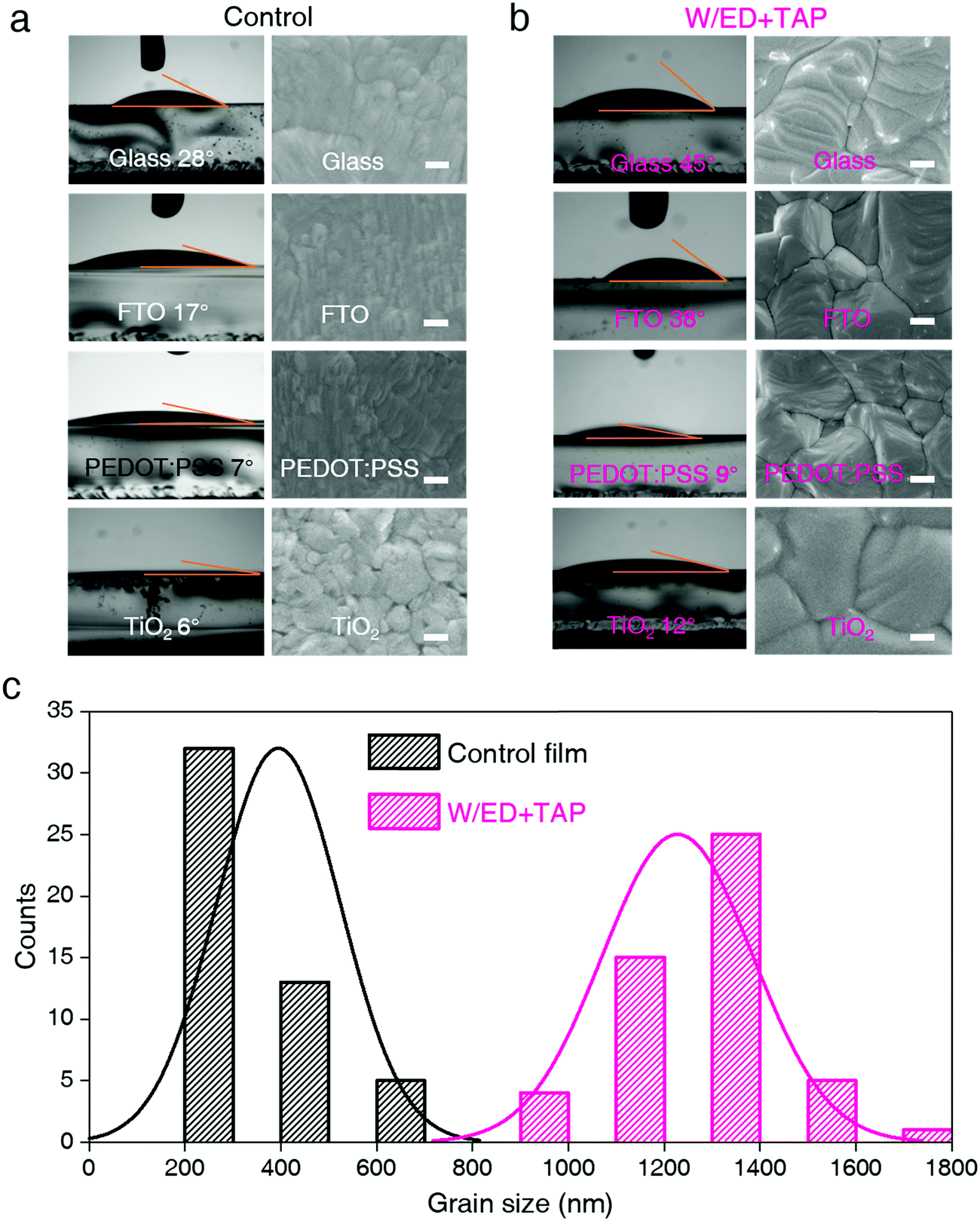 | ||
| Fig. 1 The contact angles of the (a) control and (b) W/ED+TAP precursor solution on glass, FTO, PEDOT:PSS and TiO2 surfaces and the corresponding morphologies of the perovskite films fabricated on glass, FTO, PEDOT:PSS and TiO2 surfaces, respectively. The scale bars are 200 nm. (c) The grain size distributions of the control and W/ED+TAP films on the TiO2 surface. | ||
The role of the modifiers in the precursor solution was also explored by X-ray photoelectron spectroscopy (XPS) characterization. ED contains the electron-rich atom S, while TAP contains the electron-deficient atom N. ED, TAP and their mixture were spin-coated on FTO to be investigated by XPS. As listed in Fig. S4a (ESI†), the binding energy (BE) of S 2p in the mixture is 168.73 eV, while the BE of that is 168.24 eV from ED. In comparison with pristine TAP, the BE of N 1s shifts to 402.02 eV for the mixture from 402.16 eV. These results suggest that ED interacts with TAP when mixing in the precursor solution. Since TAP contains four butyl groups, the complex of TAP and ED will increase the effect of steric hindrance, and thus the viscosity of the solution increases. We explored the viscosities of both precursor solutions, which are listed in Table S1 (ESI†). The viscosity of the W/ED+TAP precursor solution is higher than that of the control solution. It is noted that high solution viscosity causes a large surface tension force,27,28 which causes reduced grain boundary mobility. By introduction of ED and TAP, the viscosity and surface tension force of the W/ED+TAP precursor solution both increase, leading to a higher contact angle of the W/ED+TAP solution on the substrate compared to the control solution. The effect of the modifier concentration was also explored in Fig. S5 and S6 (ESI†). The results of the perovskite film fabricated using the precursor solution with pure ED or TAP are shown in Fig. S11 and S12 (ESI†). An appropriate concentration of modifiers is crucial for high-quality films and high-performance PSCs. Therefore, the appropriate concentration of ED and TAP has a positive effect on enlarging the perovskite grain size.
According to the above morphology, we speculate that the two precursor solutions with verified surface contact ability have different nucleation mechanisms (Fig. 2). The smaller contact angle of the control precursor solution on TiO2 led to a higher nucleation rate and more nuclei, which tends to heterogeneous nucleation. On the contrary, due to the larger contact angle of the W/ED+TAP solution on TiO2, homogeneous nucleation is preferred to occur.
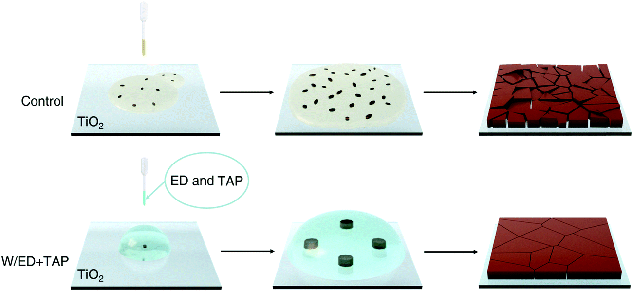 | ||
| Fig. 2 Crystal nucleation and growth mechanism of the control and W/ED+TAP films. | ||
To further explore the perovskite nucleation and growth process in the two precursor solutions, a polarizing microscope is used to observe the films during annealing at 170 °C. In Fig. 3a, the control precursor solution produces more growth sites, which continue to increase throughout the annealing process, corresponding to a high nucleation rate. For the W/ED+TAP precursor solution, fewer growth sites are produced compared with the control precursor solution. It is observed that new growth sites are hard to produce and the initial nuclei continue to grow, which tends to homogeneous nucleation. Thus, the modified precursor solution is beneficial to the formation of a large-grain perovskite.
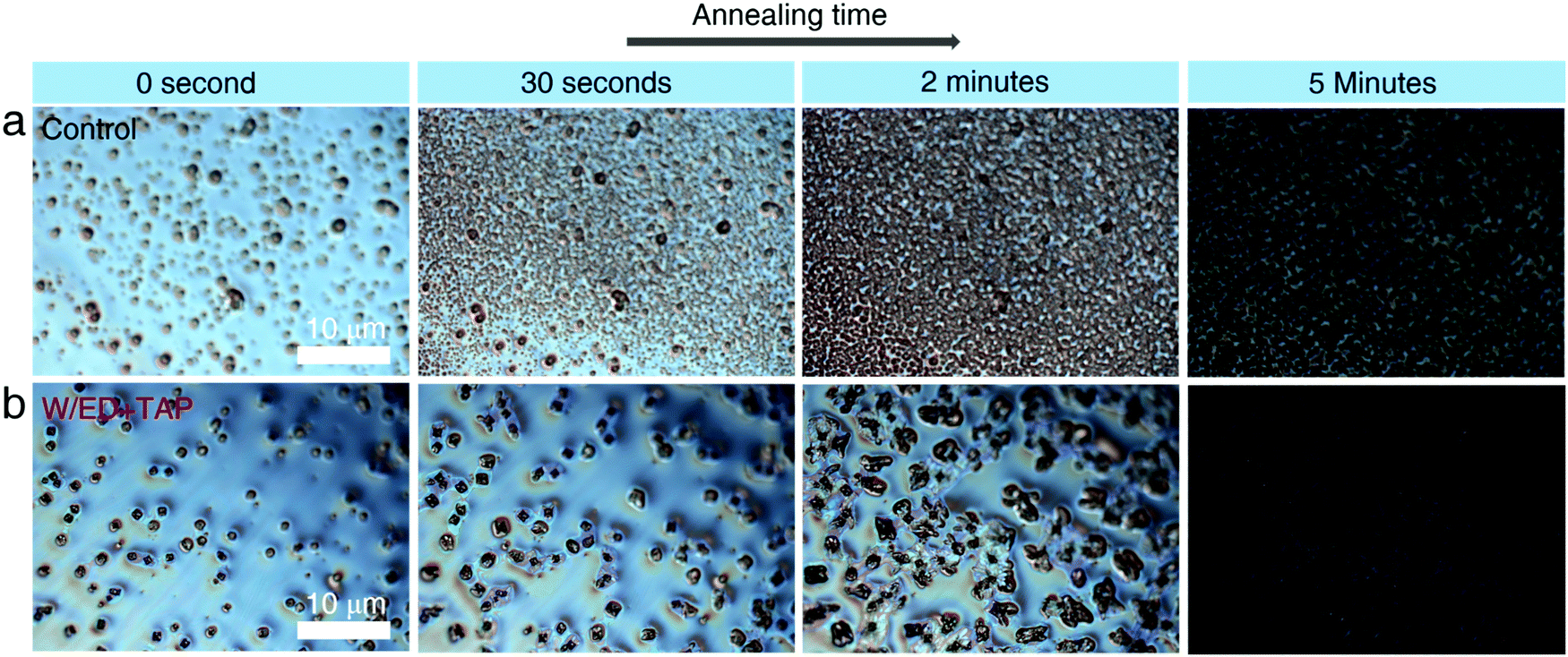 | ||
| Fig. 3 Nucleation and growth process of the (a) control perovskite and (b) W/ED+TAP perovskite. | ||
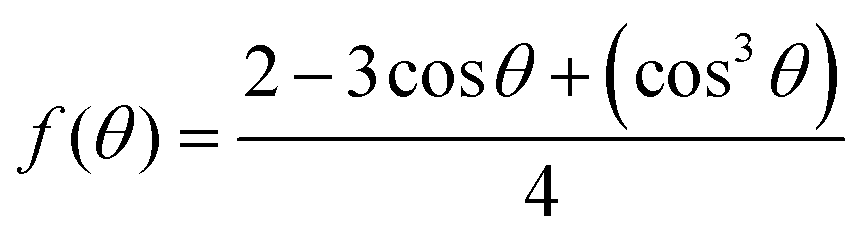
In terms of nucleation energy, the nucleation energy barrier for heterogeneous nucleation is much lower than that of homogeneous nucleation due to the shape of the nucleus. The relationship between the free energy for heterogeneous nucleation (ΔGheterogeneous) and homogeneous nucleation (ΔGhomogeneous) can be expressed by the following formula.29
| ΔGheterogeneous = ΔGhomogeneous × f(θ), |
 .
.
θ denotes the contact angle of the solid/liquid interface. Generally, both heterogeneous and homogeneous nucleation occur simultaneously in the process of perovskite nucleation. According to the formula, there exists a negative correlation between the contact angle and f(θ). When f(θ) decreases, heterogeneous nucleation is less likely to occur compared with homogeneous nucleation. Consequently, homogeneous nucleation is expected to occur more easily when the solution is deposited on substrates with larger contact angles.
Fig. S7a (ESI†) shows the ultraviolet-visible (UV-vis) absorption spectra of the perovskite films. Both of the perovskite films possess a similar absorption edge (about 830 nm) in accordance with previously reported publications.30–32 The W/ED+TAP film exhibits obviously higher absorption than the control film at wavelengths of 500–800 nm. The optical bandgaps of perovskite films are determined by Tauc's equation (αhν)2 = A(hν − Eg).31 The bandgaps of the control and W/ED+TAP films are calculated to be 1.49 eV and 1.50 eV, respectively. According to the photoluminescence (PL) spectra demonstrated in Fig. S7b (ESI†), the PL emission peak of the W/ED+TAP film is located at 812 nm, while the emission peak of the control film is located at 810 nm. This result is in agreement with the optical bandgaps derived from the UV-vis spectra. The emission intensity can be affected by the morphology and crystallinity of films according to previously reported publications.32–35 In Fig. S8 (ESI†), the control film shows the reflection peaks at 11.8°, indicating that the film contains little δ-FAPbI3. Notably, the δ-FAPbI3 peaks can hardly be seen in the XRD pattern from the W/ED+TAP film. This suggests that the modifiers in the precursor solution did not change the lattice structure or induce a new phase in the perovskite layer.
In the experiment, the PSCs are fabricated with the structure of FTO/c-TiO2/m-TiO2/perovskite/spiro-MeOTAD/Au. In Fig. 4, the photovoltaic performances of the devices based on the perovskite films coming from the two different precursor solutions are investigated. The devices are measured under standard AM 1.5G illumination at an irradiance of 100 mW cm−2 (with an active area of 0.09 cm2). Fig. 4a and Table S2 (ESI†) display the current density–voltage (J–V) curves and the corresponding photovoltaic parameters. The control device based on the control film has a PCE of 17.30%, while the W/ED+TAP device fabricated from the W/ED+TAP film shows an improved PCE of 20.15%. This result may be attributed to the high-quality and large-grained perovskite films. The improved Jsc can be observed from the incident photon to current conversion efficiency (IPCE) spectra in Fig. 4b. Moreover, there is little detected hysteresis in the reverse direction and the forward direction in Fig. S10 (ESI†). For the W/ED+TAP device, the IPCE spectrum shows over 80% from 400 nm to 700 nm and it is much higher than the control device. In addition, the reproducibility and uniformity of the PSCs are investigated. The W/ED+TAP devices exhibit the best efficiency from the PCE histograms presented in Fig. 4c. The circle represents the average values among these parameters. The W/ED+TAP devices obviously display a narrower distribution than the control devices in the parameters of FF, Voc and Jsc among the 20 devices. Thus, the high-quality and large-grained perovskite films play an important role in the device photovoltaic performance. To investigate the effect of the large grains on the defect density of the perovskite films, the defect densities are evaluated by using a FTO/c-TiO2/mp-TiO2/perovskite/PCBM/Au device structure through the space-charge-limited current (SCLC) technique.36–39 In Fig. 4d and e, the following three regions can be observed: (1) the ohmic region at low bias showing a linear relationship between the current and voltage, (2) the trap-filled limit region at intermediate bias exhibiting a steep increase in current, and (3) a trap-free (SCLC) region at high bias potential. The defect density is filled with the bias increases and all the defects are filled at the trap-filled limit voltage (VTFL). The defect density can be calculated by the equation nt = (2εε0VTFL)/(eL2), where ε, ε0, e and L refer to the dielectric constants of the perovskite, the vacuum permittivity, the elementary charge and the cross-sectional thickness of the perovskite film. Fig. S9 (ESI†) shows the cross-sectional morphology and the thickness of the perovskite film. The defect density is reduced from 1.828 × 1016 cm−3 for the control perovskite film to 1.259 × 1016 cm−3 for the W/ED+TAP perovskite film, reflecting a reduction over 30%. The defect density is obviously reduced in the large-grained perovskite films, which could be attributed to the reduced GBs of the W/ED+TAP perovskite films from the modified precursor solution.
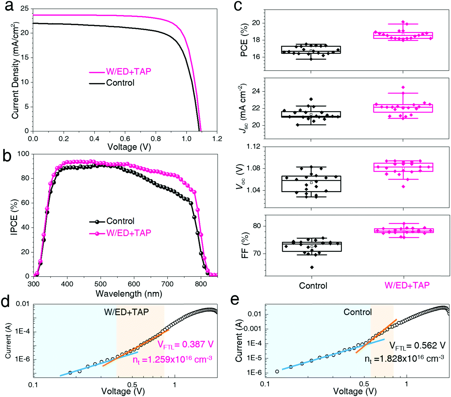 | ||
| Fig. 4 (a) J–V curves and (b) IPCE spectra of the PSCs. (c) Photovoltaic parameters from 20 PSCs devices. (d and e) Space-charge-limited current (SCLC) measurements from the two kinds of devices. | ||
Considering the fact that the humidity stability of FAPbI3 depends on the film quality of FAPbI3, the water contact angles of the control and W/ED+TAP films are tested. Fig. 5a and b show that the W/ED+TAP film achieves an improved water contact angle of 87.1°, compared to the control film (81.8°). Hence, the W/ED+TAP film has higher humidity resistance due to the high quality and large grain size. Fig. 5c exhibits the normalized PCE variation curves of the unsealed devices under 15% RH in an air atmosphere. The W/ED+TAP device can maintain 92.5% of the initial PCE after 500 hours aging time. In contrast, the control device only shows 77.6% of the initial PCE. It is supposed that enlarging the grain size of the perovskite films has a significant impact on improving the moisture resistance of photovoltaic devices.
 | ||
| Fig. 5 The water contact angles of the (a) control and (b) W/ED+TAP perovskite films. (c) Normalized PCE variation curves of the two kinds of unsealed PSCs when exposed to 15% RH. | ||
Conclusions
In summary, a modified precursor solution was demonstrated to be effective in enlarging the grain size and reducing the defect density of perovskite films by encouraging homogeneous nucleation. As a result, a micron-level grain size (∼1.7 μm) and PCE as high as 20.15% were achieved. In addition to the higher efficiency, the modified films were demonstrated to have good humidity resistance. This work provides a facile solution process to achieve high-quality, low-defect density and large-grained pure α-FAPbI3 perovskite films which possess much better optoelectronic properties. Moreover, the improved property of pure α-FAPbI3 perovskite films can offer potential applications in other fields, such as lower threshold excitation density and higher efficiency for lasers.Conflicts of interest
The authors declare no conflict of interest.Acknowledgements
This work was financially supported by the National Key R&D Program of China (No. 2019YFB1503200), National Natural Science Foundation of China (Grant No. 11904366) and the CASHIPS Director's Fund (Grant No. YZJJ2019QN16).References
- A. Kojima, K. Teshima, Y. Shirai and T. Miyasaka, J. Am. Chem. Soc., 2009, 131, 6050–6051 CrossRef CAS.
- M. Liu, M. B. Johnston and H. J. Snaith, Nature, 2013, 501, 395–398 CrossRef CAS.
- H. Y. Zheng, W. W. Wu, H. F. Xu, F. C. Zheng, G. Z. Liu, X. Pan and Q. W. Chen, Adv. Funct. Mater., 2020, 30, 2000034 CrossRef CAS.
- G. Z. Liu, H. Y. Zheng, H. F. Xu, L. Y. Zhang, X. X. Xu, S. D. Xu and X. Pan, Nano Energy, 2020, 73, 104753 CrossRef CAS.
- Y. K. Ren, X. H. Ding, Y. H. Wu, J. Zhu, T. Hayat, A. Alsaedi, Y. F. Xu, Z. Q. Li, S. F. Yang and S. Y. Dai, J. Mater. Chem. A, 2017, 5, 20327–20333 RSC.
- H. Y. Zheng, G. Z. Liu, L. Z. Zhu, J. J. Ye, X. X. Zhang, A. Alsaedi, T. Hayat, X. Pan and S. Y. Dai, Adv. Energy Mater., 2018, 8, 1800051 CrossRef.
- J. Burschka, N. Pellet, S. J. Moon, R. Humphry-Baker, P. Gao, M. K. Nazeeruddin and M. Gratzel, Nature, 2013, 499, 316–319 CrossRef CAS.
- H. D. Kim, H. Ohkita, H. Benten and S. Ito, Adv. Mater., 2016, 28, 917–922 CrossRef CAS.
- Z. Xiao, Q. Dong, C. Bi, Y. Shao, Y. Yuan and J. Huang, Adv. Mater., 2014, 26, 6503–6509 CrossRef CAS.
- Y. Zhang, S. G. Kim, D. Lee, H. Shin and N. G. Park, Energy Environ. Sci., 2019, 12, 308–321 RSC.
- Q. Dong, Y. Fang, Y. Shao, P. Mulligan, J. Qiu, L. Cao and J. Huang, Science, 2015, 347, 967–970 CrossRef CAS.
- D. Zhao, M. Sexton, H. Y. Park, G. Baure, J. C. Nino and F. So, Adv. Energy Mater., 2015, 5, 1401855 CrossRef.
- G. E. Eperon, V. M. Burlakov, P. Docampo, A. Goriely and H. J. Snaith, Adv. Funct. Mater., 2014, 24, 151–157 CrossRef CAS.
- B. Conings, L. Baeten, C. De Dobbelaere, J. D'Haen, J. Manca and H. G. Boyen, Adv. Mater., 2014, 26, 2041–2046 CrossRef CAS.
- D. Bi, C. Yi, J. Luo, J. Décoppet, F. Zhang, S. Zakeeruddin, X. Li, A. Hagfeldt and M. Grätzel, Nat. Energy, 2016, 1, 16142 CrossRef CAS.
- B. Yang, O. Dyck, J. Poplawsky, J. Keum, A. Puretzky, S. Das, I. Ivanov, C. Rouleau, G. Duscher, D. Geohegan and K. Xiao, J. Am. Chem. Soc., 2015, 137, 9210–9213 CrossRef CAS.
- Y. Shao, Z. Xiao, C. Bi, Y. Yuan and J. Huang, Nat. Commun., 2014, 5, 5784 CrossRef CAS.
- L. Wang, C. McCleese, A. Kovalsky, Y. Zhao and C. Burda, J. Am. Chem. Soc., 2014, 136, 12205–12208 CrossRef CAS.
- Q. Chen, H. Zhou, T. B. Song, S. Luo, Z. Hong, H. S. Duan, L. Dou, Y. Liu and Y. Yang, Nano Lett., 2014, 14, 4158–4163 CrossRef CAS.
- N. K. Noel, A. Abate, S. D. Stranks, E. S. Parrott, V. M. Burlakov, A. Goriely and H. J. Snaith, ACS Nano, 2014, 8, 9815–9821 CrossRef CAS.
- C. Bi, Q. Wang, Y. Shao, Y. Yuan, Z. Xiao and J. Huang, Nat. Commun., 2015, 6, 7747 CrossRef CAS.
- H. Zhou, Q. Chen and Y. Yang, MRS Bull., 2015, 40, 667–673 CrossRef CAS.
- X. Li, D. Bi, C. Yi, J. Décoppet, J. Luo, S. Zakeeruddin, A. Hagfeldt and M. Grätzel, Science, 2016, 353, 58–62 CrossRef CAS.
- J. M. Ball, M. M. Lee, A. Hey and H. J. Snaith, Energy Environ. Sci., 2013, 6, 1739–1743 RSC.
- S. Park, H. Cho, W. Choi, H. Zou and D. Y. Jeon, Nanoscale Adv., 2019, 1, 2785–3290 RSC.
- L. Ruan, W. Shen, A. Wang, Q. Zhou, H. Zhang and Z. Deng, Nanoscale, 2017, 9, 7252–7259 RSC.
- H. Song, X. Wang, Y. Tan and Y. Liu, Guangzhou Chem., 2002, 27, 10–13 CAS.
- S. Auer and D. Frenkel, Nature, 2001, 413, 711 CrossRef CAS.
- T. Salim, S. Sun, Y. Abe, A. Krishna, A. C. Grimsdale and Y. M. Lam, J. Mater. Chem. A, 2015, 3, 8943–8969 RSC.
- W. Yang, B. Park, E. Jung, N. Jeon, Y. Kim, D. Lee, S. Shin, J. Seo, E. Kim, J. Noh and S. Soek, Science, 2017, 356, 1376–1379 CrossRef CAS.
- W. Yang, J. Noh, N. Jeon, Y. Kim, S. Ryu, J. Seo and S. Seok, Science, 2015, 348, 1234–1237 CrossRef CAS.
- Q. Jiang, L. Zhang, H. Wang, X. Yang, J. Meng, H. Liu, Z. Yin, J. Wu, X. Zhang and J. You, Nat. Energy, 2016, 2, 16177 CrossRef.
- Z. Wang, Q. Lin, F. P. Chmiel, N. Sakai, L. M. Herz and H. J. Snaith, Nat. Energy, 2017, 2, 17135 CrossRef CAS.
- X. Xu, Z. Li, L. Zhu, H. Zheng, G. Liu, T. Hayat, A. Alsaedi, X. Zhang, Y. Huang and X. Pan, J. Mater. Chem. A, 2019, 7, 1341–1348 RSC.
- K. Tvingstedt, O. Malinkiewicz, A. Baumann, C. Deibel, H. J. Snaith, V. Dyakonov and H. J. Bolink, Sci. Rep., 2014, 4, 6071 CrossRef CAS.
- D. Shi, V. Adinolfi, R. Comin, M. Yuan, E. Alarousu, A. Buin, Y. Chen, S. Hoogland, A. Rothenberger, K. Katsiev, Y. Losovyj, X. Zhang, P. A. Dowben, O. F. Mohammed, E. H. Sargent and O. M. Bakr, Science, 2015, 347, 519–522 CrossRef CAS.
- J. Chen, S. G. Kim, X. Ren, H. S. Jung and N. G. Park, J. Mater. Chem. A, 2019, 7, 4977–4987 RSC.
- Y. K. Ren, J. Chen, D. H. Ji, Y. J. Sun and C. Li, Chem. Eng. J., 2020, 385, 123273 CrossRef.
- Q. Chen, H. Zhou, Z. Hong, S. Luo, H. S. Duan, H. H. Wang, Y. Liu, G. Li and Y. Yang, J. Am. Chem. Soc., 2014, 136, 622–625 CrossRef CAS.
Footnote |
| † Electronic supplementary information (ESI) available. See DOI: 10.1039/d0tc04833j |
| This journal is © The Royal Society of Chemistry 2021 |