
Facile fabrication of ultrathin graphene film with ultrahigh electrical conductivity and superb electromagnetic interference shielding effectiveness†
Xiaojing
Liu
,
Wenyu
Wu
,
Bin
Guo
,
Minghao
Cui
,
Huaxin
Ma
,
Zhao
Zhang
and
Ruijun
Zhang
 *
*
State Key Laboratory of Metastable Materials Science and Technology, Yanshan University, Qinhuangdao 066004, China. E-mail: zhangrj@ysu.edu.cn; Tel: +86 335 8074631
First published on 19th November 2020
Abstract
Graphene films prepared through a self-assembly of graphene oxide and its derivatives have been recently explored for electromagnetic interference (EMI) shielding applications. However, this film preparation usually requires long-time high-temperature annealing, leading to a dramatic increase in energy and time-consumption and thus the total cost of mass production. Herein, a free-standing, highly flexible and conductive graphene film was fabricated via a simple and inexpensive method. The fabrication process starts with the chemical exfoliation of graphite in a novel binary-component system comprised of sodium peroxyborate and sulfuric acid, as a graphene suspension, which is then vacuum-filtered and mechanically pressed, not involving high-temperature post-treatment. The obtained graphene film shows excellent electrical conductivity of 1.53 × 10⁶ S m−1. More importantly, it also exhibits an ultrahigh EMI SE of 68 dB at a frequency of 8.2–12.4 GHz, which can block 99.99999% of incident radiation. To the best of our knowledge, this is the highest EMI SE performance reported so far in such thin thickness (about 3.2 μm) of pure graphene materials. These outstanding properties make this ultrathin graphene film a promising alternative building block for electronic devices.
Introduction
With the rapid development of electronic devices, ultrathin and lightweight electromagnetic interference (EMI) shielding materials with high shielding effectiveness (SE) are highly needed for many applications.1–4 Generally speaking, the permeability and electrical conductivity of a material are two crucial factors affecting its EMI shielding performance.5,6 Up to now, many efforts have been made to improve the EMI SE of a material by regulating its permeability.7–9 On the other hand, since high electrical conductivity is beneficial to the EMI shielding performance, the materials having excellent conductivity are usually applied in the EMI shielding field. For example, traditional metals have been used as the EMI shielding materials.10 However, they commonly suffer from the drawbacks of high density, low corrosion resistance, etc.11Graphene, as a two-dimensional nanomaterial, is very promising for EMI shielding applications due to its low density, excellent mechanical properties and high electrical conductivity. Seul K et al. firstly reported their investigation into the EMI shielding application of single-layered CVD graphene, and found that the obtained EMI SE value is 2.27 dB, approximately seven times higher than that of Au film.12 Then, the EMI shielding performance for thick CVD graphene film was further studied, which gave improved shielding effectiveness up to ≈60 dB.13 Despite the better EMI shielding performance, CVD-produced graphene film still lacks competitiveness for practical applications, due to the disadvantages of high cost and the complex hardware system. In this context, the low-cost graphene oxide (GO) seems more suitable as a precursor to fabricate graphene film for the EMI shielding applications. Up to now, the EMI shielding performance of the graphene films prepared through the self-assembly of GO and its derivatives have been extensively explored.14–16 However, the GO preparation involves the use of strong oxidizing agent, which leads to serious structural defects and thus poor electrical performance of graphene. To improve the electrical conductivity of the graphene film fabricated by the GO self-assembly, a long-time high-temperature annealing at 1000–3000 °C is necessarily needed, which will dramatically increase the time and energy consumption and thus the total cost. Therefore, facile preparation methods for high-quality graphene films with high conductive and electromagnetic shielding properties are still urgently desired.
Exfoliation from graphite into graphene via a relatively moderate chemical system, including H2SO4/(NH4)2S2O8,17 H2SO4/Na2S2O8,18 H2SO4/H2O2,19 H2SO4/CH3COOOH,20etc., is much simpler and more cost-effective than the GO preparation route. More importantly, this method has also the prominent advantage in preparing high-quality graphene with few defects and a large size. Unfortunately, the excessive usage of concentrated H2SO4 in these conventional methods can lead to the environmentally detrimental impact caused by the effluent of the waste acid.19 In the present work, we developed a novel chemical system for the exfoliation of graphite to graphene, which is comprised of sodium peroxyborate (BH8NaO7) and sulfuric acid, and BH8NaO7 is used to exfoliate the graphite for the first time. Compared with conventional chemical exfoliation methods, the H2SO4 amount used in this new system is decreased by about 80% or more.17–20 More interestingly, during the investigation into optimizing the chemical exfoliation procedure of graphene in the system, we have found that pre-soaking the pristine graphite with H2SO4 can promote the more sufficient exfoliation of graphite, thus obtaining graphene sheets with less defects, fewer layers and larger areal size. Furthermore, the ultrathin graphene film with approximately 3.2 μm only in thickness, which was fabricated by using a simple vacuum filtration method from the obtained graphene solution without the high-temperature post-treatment, has shown outstanding electrical conductive and EMI performances. Its electrical conductivity is up to 1.53 × 10⁶ S m−1 and EMI SE is 68 dB, both higher than the values reported previously. This method has great potential in satisfying the increasing needs for EMI shielding in electronic devices, while dramatically reducing the preparation time, energy consumption and thus the processing costs.
Experimental section
1. Preparation of graphene samples
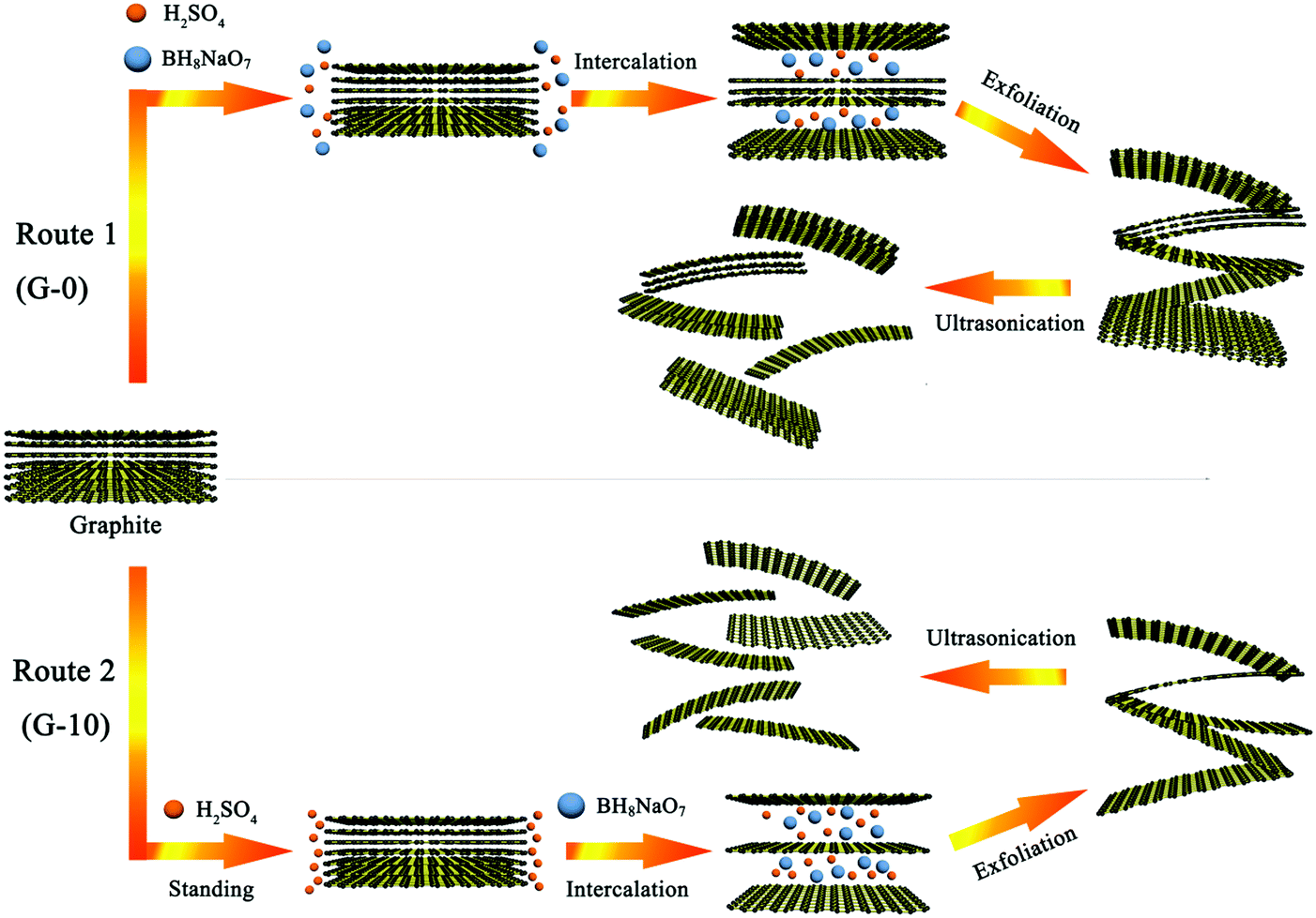
In this work, two technical routes have been employed to chemically exfoliate natural graphite (NG, 50 meshes) into graphene in a binary-component system made by a combination of sodium perborate (BH8NaO7) and concentrated H2SO4. Route 1 is described as follows: firstly, 0.25 g of NG and 4 ml of concentrated H2SO4 (98%) were added into a 20 ml beaker and stirred at room temperature for a couple of seconds until well mixed, acquiring a binary–component mixture. Then 1 g of BH8NaO7 was added to the mixture and stirred for 30 s, thus obtaining a ternary–component mixture. After keeping in a drying oven at 50 °C for 2 h, this mixture was completely transformed into loose and porous graphene aggregates (GAs). The GAs were washed with deionized water until pH = 6, then ultrasonically dispersed (70 W, 20 min) in ethanol and dried at 60 °C, thereby obtaining the prepared graphene sheets (G-0).As for route 2 (also called the pre-soaking route, newly developed in this work), the distinct difference from route 1 is that, after the binary–component mixture consisting of NG (0.25 g) and concentrated H2SO4 (4 ml) is well prepared, it is intentionally placed in a low temperature environment of 6 °C and stood for 10 h. Thereafter, this mixture would be further treated according to the procedures described in route 1, including the addition of BH8NaO7, heat treatment at 50 °C, water-washing, ultrasonication, etc. The eventually obtained graphene sample is denoted as G-10.
2. Preparation of flexible graphene thin films
The as-prepared graphene samples (G-0 and G-10) were sufficiently dispersed in a water–ethanol mixture (H2O–EtOH, 1![[thin space (1/6-em)]](https://www.rsc.org/images/entities/char_2009.gif) :4 in mass) under 100 W ultrasonication for 20 min, respectively, thus acquiring two graphene dispersions. Next, the graphene films were, respectively, prepared by vacuum-filtrating the G-0 and G-10 dispersions through polyethersulfone (PES) membranes (0.22 um in pore size), followed by drying at room temperature for 24 h. Thereafter, the two graphene films were mechanically pressed under 20 MPa and transferred into DMF solvent to dissolve the PES membrane and then dried at 60 °C for 12 h, eventually obtaining the flexible graphene thin film samples – F-0 and F-10.
:4 in mass) under 100 W ultrasonication for 20 min, respectively, thus acquiring two graphene dispersions. Next, the graphene films were, respectively, prepared by vacuum-filtrating the G-0 and G-10 dispersions through polyethersulfone (PES) membranes (0.22 um in pore size), followed by drying at room temperature for 24 h. Thereafter, the two graphene films were mechanically pressed under 20 MPa and transferred into DMF solvent to dissolve the PES membrane and then dried at 60 °C for 12 h, eventually obtaining the flexible graphene thin film samples – F-0 and F-10.
3. Characterization
X-ray diffraction (XRD) data were collected on an X-ray diffractometer (Rigaku D/MAX-2500) with Cu-Kα radiation (λ = 0.154 nm) operated at 40 kV and 200 mA. Raman spectra were obtained using a Renishaw inVia™ Raman microscope with a 532 nm laser wavelength. The morphology of the samples was observed by field emission scanning-electron microscopy (SEM, Hitachi S-4800) at 15 kV. Transmission electron microscopy (TEM) images were taken on a Talos F200X at 200 kV. In addition, the electrical conductivity of the graphene sample was measured by using the standard four-point probe technique. Electromagnetic interference (EMI) shielding properties at different frequencies (X-band: 8.2–12.4 GHz frequency) were conducted on an Agilent N5244A vector network analyzer. The graphene film specimens were carefully cut into 22.9 × 10.9 mm2 strips to well fit the specific waveguide holders (X band).Results and discussion
1. Characterization of graphene
Fig. 1 illustrates schematically the evolution process of graphite to graphene aggregates (GAs) by chemical exfoliation according to route 2. It can be found that, after treating at 50 °C for 2 h, the ternary mixture, which is comprised of NG (0.25 g), concentrated H2SO4 (4 ml) and BH8NaO7 (1 g), has been completely dried and develops huge expansion with a worm-like structural character, suggesting that all the NG flakes have been transformed completely into the loosely porous GAs. Interestingly, no liquid H2SO4 remained in the obtained GAs, which will greatly alleviate the environmentally detrimental impact caused by the effluent of the waste acid.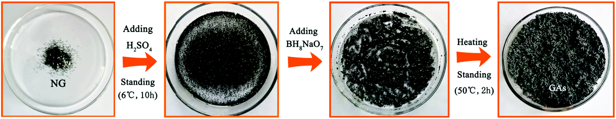 | ||
| Fig. 1 Schematic illustration of the evolution process from graphite to GAs by chemical exfoliation according toroute 2. | ||
Two graphene samples – G-0 and G-10 were obtained by low-power ultrasonication from the resultant GAs, which were prepared by routes 1 and 2, respectively. Fig. 2a shows the XRD patterns of NG, G-0 and G-10. The (002) and (004) diffraction peaks located at 26.3°and 54.4°, respectively, can be clearly observed on the XRD pattern of NG, revealing its high crystallinity. However, both the (002) and (004) diffraction signals of G-0 and G-10 become dramatically weaker. This can be considered as an indication of the few-layer feature and the positional disorder in the graphene nanosheets caused by the exfoliation of the graphite layers,21–23 demonstrating that the as-prepared G-0 and G-10 samples have few layers in the stack. Furthermore, it can be observed that G-10 behaves with a weaker (002) peak intensity than that of G-0, confirming that the pre-soaking treatment with H2SO4 can facilitate the more sufficient exfoliation of graphite and the achievement of thinner graphene nanosheets.
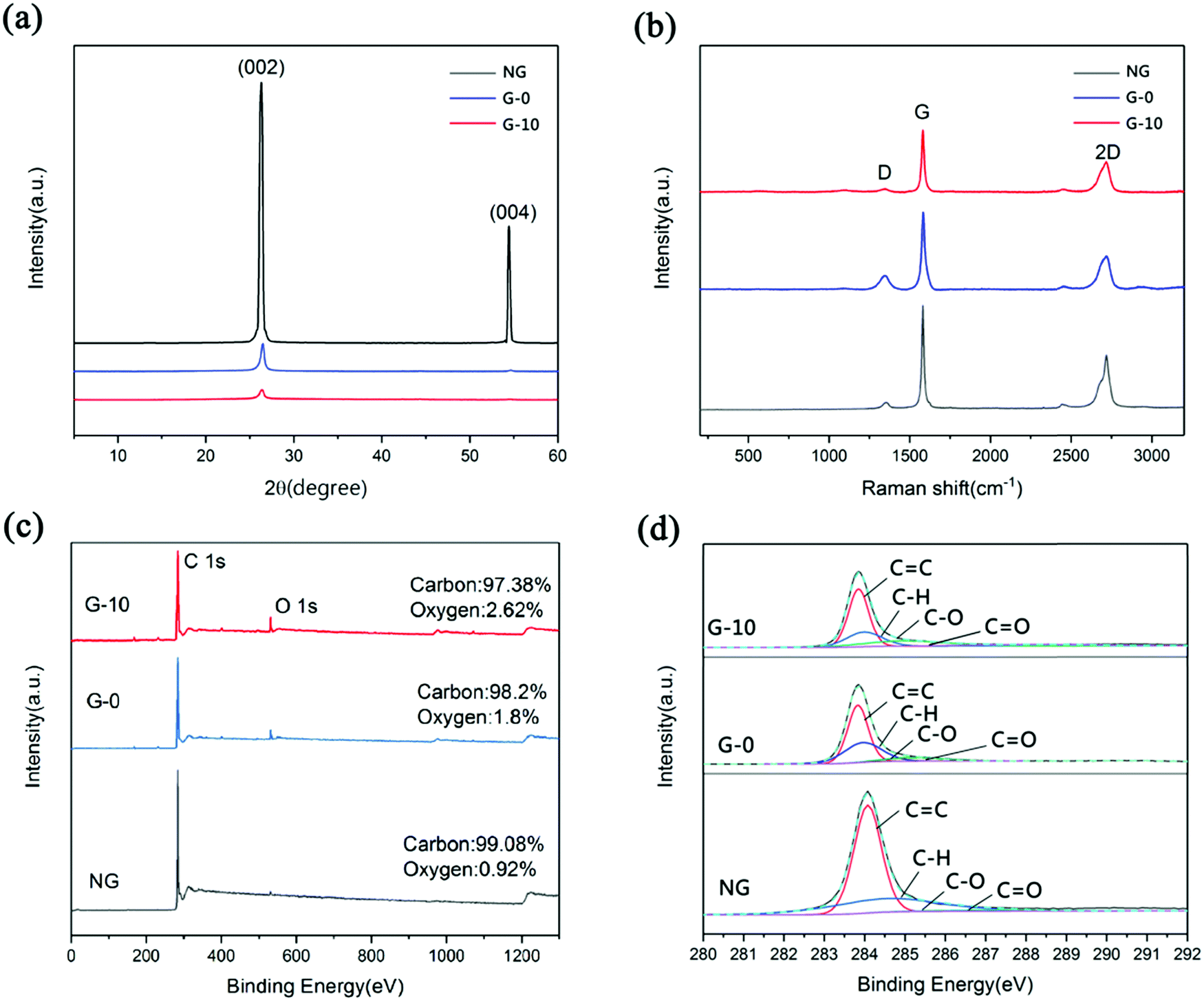 | ||
| Fig. 2 (a) XRD patterns of NG, G-0 and G-10; (b) Raman spectra of NG, G-0 and G-10; (c) XPS survey spectra of NG, G-0 and G-10; (d) C 1s spectra of NG, G-0 and G-10. | ||
The obtained graphene powders were also characterized by Raman spectroscopy, as displayed in Fig. 2b. Three typical characteristic peaks – D (∼1350 cm−1), G (∼1580 cm−1) and 2D (∼2700 cm−1) peaks occur clearly in the Raman spectra of NG, G-0 and G-10. Usually, the ID/IG value provides a measure of defects in the graphene samples, and the defect density is directly proportional to the ID/IG value.23–27 In this study, the calculated ID/IG values for NG, G-0 and G-10 are 0.07, 0.18 and 0.08, respectively. This result implies that the structural integrity of NG can be effectively retained in the G-10 sample, suggesting that the pre-soaking treatment with H2SO4 can facilitate the achievement of graphene with lower defect density. Besides, the I2D/IG value is commonly used as a quantitative guide to distinguish the layer number, and, a higher I2D/IG value implies a fewer layer number in graphene.28,29 Therefore, based on their Raman spectra, we can calculate the I2D/IG values for G-0 and G-10 to be 0.46 and 0.58, respectively, further demonstrating that the pre-soaking treatment with H2SO4 can facilitate the achievement of thinner graphene nanosheets.
We used X-ray photoelectron spectroscopy (XPS) to further study the elemental compositions, contents and chemical states of the graphene samples. As shown in Fig. 2(c), the C1s (284.8 eV) and O1s (532.3eV) peaks could be observed on the XPS survey spectra of NG, G-0 and G-10, suggesting the existence of O element in all the three samples. The calculated O contents for G-0 and G-10 are 1.8 and 2.62%, respectively, both higher than that of NG (0.92%), suggesting the introduction of O-species onto the obtained graphene. To identify the type of the O-species during the chemical exfoliation, we fit the C1s peaks by the Gaussian–Lorentzian function, as displayed in Fig. 2(d). Obviously, the C1s spectra of NG, G-0 and G-10 could be fitted by four binding energies of 284.6 eV, 285.4 eV, 286.5 eV and 288.9 eV, corresponding to the C![[double bond, length as m-dash]](https://www.rsc.org/images/entities/char_e001.gif) C, C–H, C–O and CO bonds, respectively. The result reveals the similar oxygen species existing in the starting graphite and the obtained graphene nanosheets.
C, C–H, C–O and CO bonds, respectively. The result reveals the similar oxygen species existing in the starting graphite and the obtained graphene nanosheets.
To further investigate the morphological characteristics of the samples, SEM observation was performed, as displayed in Fig. 3a–c. The morphological transformation from the lamellar stacking structure (NG, Fig. 3a) to the highly delaminated morphology (G-0 and G-10, Fig. 3b and c) clearly reveals the high-yield transformation of graphite to few-layer graphene sheets. Moreover, both the SEM images of G-0 and G-10 clearly exhibit a transparent feature in the electron beam, suggesting their few-layer behaviour.
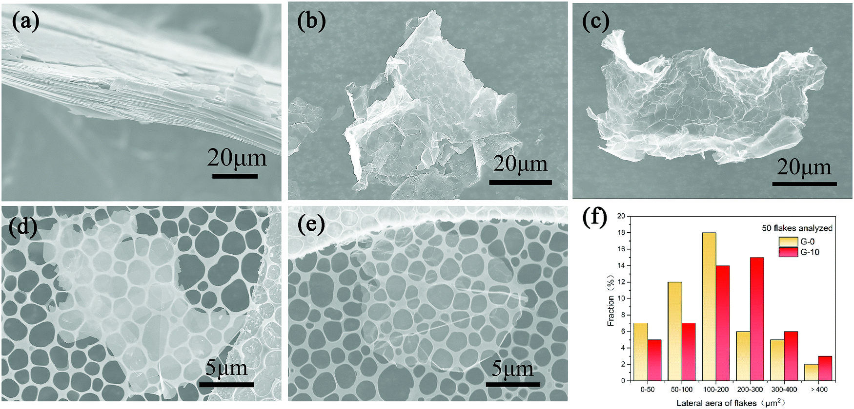 | ||
| Fig. 3 SEM images of (a) NG, (b) G-0, (c) G-10, and (d) G-0 dispersed on the TEM micro-grid. (e) G-10 dispersed on the TEM micro-grid. (f) Lateral area distribution of graphene calculated from 50 flakes. | ||
Furthermore, to determine the size range of graphene sheets, we dispersed the obtained G-0 and G-10 powders in absolute ethyl alcohol under low-power sonication (70 W) and deposited the graphene dispersion on the TEM micro-grid for SEM observation. Fig. 3d and e display the typical SEM images of the as-dispersed G-0 and G-10 samples. Comparatively, G-10 is obviously more transparent than G-0, implying that it has fewer layers in the stack, which is in good agreement with the aforementioned XRD and Raman results (Fig. 2a and b). By measuring the lateral dimensions of 50 graphene sheets, we created a size distribution bar chart, as shown in Fig. 3f. From which, it can be deduced that the average areal sizes of G-0 and G-10 are 140 and 260 μm2, respectively. Interestingly, about 46% of the obtained nanosheets for G-10 are larger than 150 μm2, far higher than those for G-0 (26%) and other graphene samples (16% or less) reported previously.18–20 This result proves that the pre-soaking treatment with H2SO4 can effectively avoid the serious damage to natural graphite flakes and thus facilitate the achievement of graphene sheets with a larger areal size.
AFM measurement was further employed to assess the obtained G-0 and G-10 samples, as exemplarily shown in Fig. 4a and b. Their thickness distribution based on the measurement of 50 graphene nanosheets is shown in Fig. 4c and d, respectively. From which, it can be deduced that the average thicknesses of the as-obtained graphene sheets for G-0 and G-10 samples are ∼3.12 and 1.26 nm, corresponding to ∼8 and 3 layers, respectively.
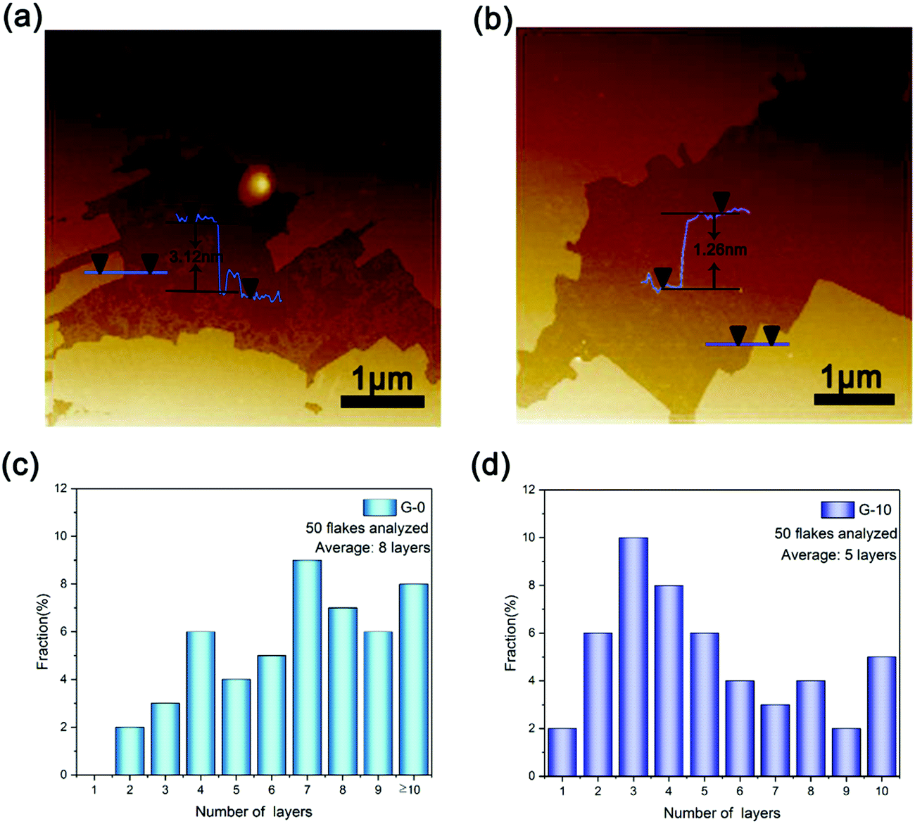 | ||
| Fig. 4 Characterization of the graphene. (a) AFM image of G-0 (inset is the height profile taken across the blue line on the AFM image); (b) AFM image of G-10 (inset is the height profile taken across the purple line on the AFM image); (c) layer distribution determined by AFM statistics of G-0; (d) layer distribution determined by AFM statistics of G-10. | ||
In our present research, it is revealed that, when the H2SO4 and BH8NaO7 system is used to chemically exfoliate graphite into graphene, the pre-soaking treatment with H2SO4 can result in the achievement of fewer layer-number graphene. This finding is interesting but further investigation into the underlying mechanism is needed. For this novel chemical exfoliation system, the possible exfoliation mechanism may be briefly described as follows: when NG is mixed in the H2SO4/BH8NaO7 solution, BH8NaO7 oxidizes the NG edges, thus enabling H2SO4 to intercalate into the path of graphite interlayers. During the H2SO4 intercalation, it will drag parts of the excess BH8NaO7 into the path. Then, the chemical instability will cause the dragged BH8NaO7 to decompose and release O2 gas, which will lead to an instantaneous gas pressure rise within the NG path, thereby generating the exfoliation of graphite. As for the newly-developed pre-soaking strategy, the NG powders are firstly soaked in the H2SO4 solution for a long duration, during which, more edges of the graphitic structure will have enough time to be sufficiently wetted by H2SO4 molecules. In this case, it will be possible for more galleries of graphite to be intercalated by H2SO4. Therefore, after BH8NaO7 is added into the H2SO4-soaked NG mixture and the graphite edges are oxidized, H2SO4 (with the BH8NaO7 dragged) will intercalate into more graphitic galleries. As a result, the release of O2 gas within more graphitic galleries, due to the decomposition of the dragged BH8NaO7, will facilitate more sufficient exfoliation of graphite, thus resulting in the achievement of graphene with fewer layers. A schematic illustration of the effect of pre-soaking is given in Scheme 1.
 | ||
| Scheme 1 Schematic illustration of the synthesis of G-0 and G-10. | ||
2. Electrical and electromagnetic shielding performances of graphene films
Two graphene films (F-0 and F-10) were, respectively, assembled from the G-0 and G-10 graphene dispersion in a water–ethanol mixture by simple vacuum filtration and room-temperature mechanical pressing. By means of the SEM observation, we can determine that both the films are about 1.6 μm thick with a well-aligned stacking structure (Fig. 5a). Moreover, these two graphene films are very lightweight (Fig. 5b), and can be easily rolled (Fig. 5c) and folded into a small boat-like shape with no crack or fracture (Fig. 5d), demonstrating their superior flexibility. Furthermore, the electrical conductivities of the prepared graphene films were measured with a four-probe method, as displayed in Fig. 5e. The average electrical conductivities for F-0 and F-10 are 0.88 × 10⁶ and 1.53 × 10⁶ S m−1, respectively. This superior conductivity of the F-10 film is also verified by the fact that the brightness of a small light bulb connected to the F-10 strip (1 × 2cm in size) is significantly stronger than that of the bulb connected to the similar sized F-0 strip (insets, Fig. 5e). Fig. 5f displays the XRD patterns of F-0 and F-10 films, respectively. According to the XRD pattern, the FWHM values of F-0 and F-10 can be calculated as 0.436 and 0.407, respectively. Since a smaller FWHM value indicates that the graphitic structure is more orderly,30,31 we can conclude that F-10 has a better structural ordering than F-0. This may be one of the reasons for the excellent electrical performance of F-10.32 Here, it is worth noting that this electrical conductivity value for F-10 is far higher than those for graphene films reported so far.25–27,33–35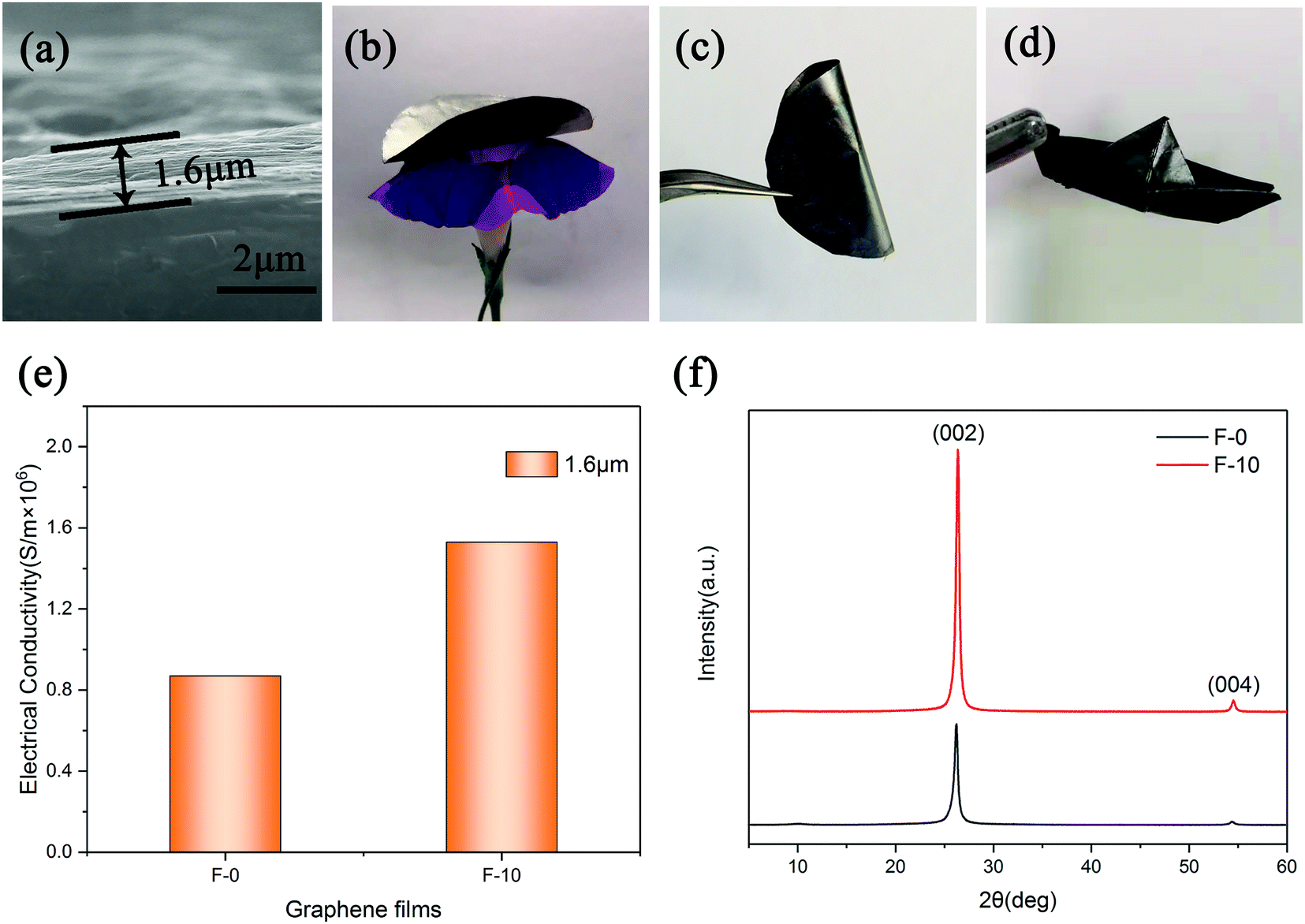 | ||
| Fig. 5 (a) Cross-sectional SEM view of the graphene film; (b) digital image of the graphene film; (c) digital image presenting the flexibility; (d) a film was folded into the shape of a small boat; (e) the electrical conductivities of F-0 and F-10; (f) XRD spectra of F-0 and F-10. | ||
Generally, graphene films with large electrical conductivity have high EMI SE values.36–40 So, this ultra-high electrical conductivity for F-10 may suggest its great potential in EMI shielding applications. For this reason, the measurement of EMI shielding performance for the F-10 films having a thickness of 1.6 and 3.2 μm, respectively, was further performed in the X-band range (8.2–12.4 GHz) using a vector network analyzer, and the corresponding results are shown in Fig. 6a. The average EMI SE values of the F-10 films having thicknesses of 1.6 and 3.2 μm are 33 and 68 dB, respectively. This result should be reasonable, since the thick graphene film can effectively consume more electromagnetic waves and thus exhibit superior EMI shielding performance.25 For clarification of the shielding mechanism, comparison of the total EMI shielding effectiveness (SETotal), microwave absorption (SEA) and microwave reflection (SER) values of films with thicknesses of 1.6 μm and 3.2 μm at a constant frequency of 10.3 GHz was investigated, as shown in Fig. 6b. It can be seen that the SEA values for both the F-10 films has more contribution than SER to the SEtotal value, which clarifies that the absorption of microwaves dominates the EMI shielding mechanism and the majority of microwaves are absorbed due to the extraordinary electrical conductivity of F-10. Moreover, the SEA/SETotal values for the 1.6 μm and 3.2 μm thick films are calculated as 51% and 75%, respectively, indicating that the shielding due to absorption will become the most crucial factor in determining the EMI performance with the increase of film thickness. Furthermore, it is worth mentioning that the EMI SE performance (68 dB) for the 3.2 μm-thick F-10 film is enough to obstruct and absorb 99.99999% of incident radiation with only 0.00001% transmission. To the best of our knowledge, this is the highest EMI SE performance reported so far in such a thin thickness (about 3.2 μm) of typical shielding materials (Table 1).
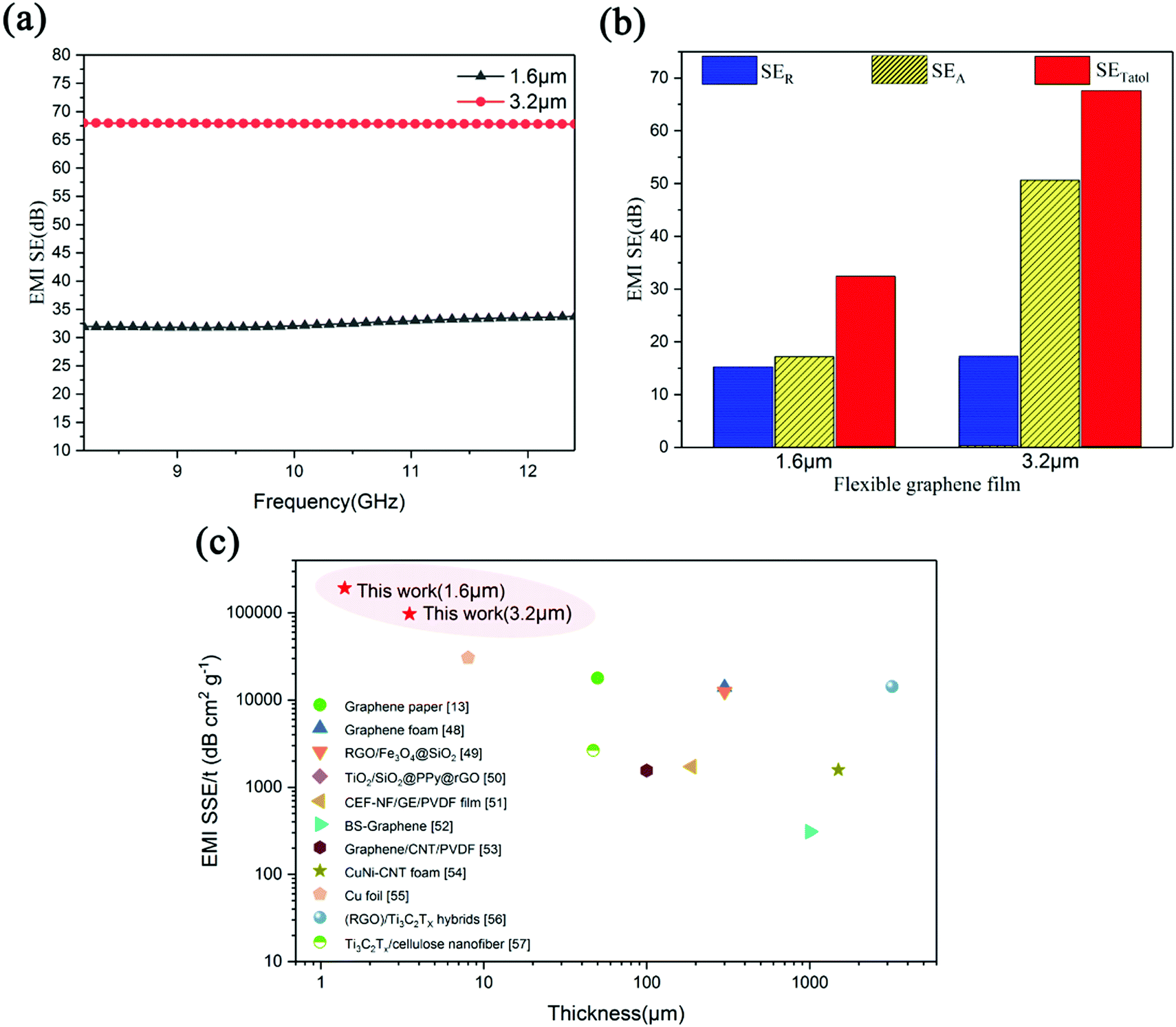 | ||
| Fig. 6 (a) EMI shielding properties in the frequency range of 8.2∼12.4 GHz with different film thicknesses; (b) total EMI SE (EMI SET) and its absorption (SEA) and reflection (SER) mechanism in F-10 samples at 10.3 GHz; (c) comparison of EMI SSE/t of typical materials with different thicknesses. | ||
| Samples | Thickness (um) | Electrical conductivity (S m−1) | SEtotal (dB) | Frequency (GHz) | Ref. |
|---|---|---|---|---|---|
| GAF | 50 | 6600 | 45 | 0.1–3 | 41 |
| EG films | 10 | 2.977 × 10⁵ | 33.1 | 8.2–12.4 | 42 |
| Iodine-doped LG paper | 12.5 | 1.05 × 10⁵ | 52.2 | 8.2–12.4 | 25 |
| Graphene paper | 50 | 1.136 × 10⁵ | 60 | 8.2–12.4 | 13 |
| GCF | 15 | 2.74 × 10⁵ | 60 | 2–18 | 43 |
| S-GNS | 300 | 1333 | 34.4 | 8.2–12.4 | 44 |
| PGFs | 200 | 600 | 63 | 8.2–12.4 | 45 |
| rGO-EDA-2 | 6.6 | 8.796 × 10⁵ | 58.5 | 8.2–12.4 | 46 |
| EG/CNF/PEO film | 12 | 1.226 × 10⁵ | 44 | 8.2–12.4 | 40 |
| F-10 | 1.6 | 1.53 × 10 6 | 33 | 8.2–12.4 | This work |
| F-10 | 3.2 | 2.77 × 10 6 | 68 | 8.2–12.4 | This work |
It is worth pointing out that the EMI shielding materials, which have reduced weight and thickness while maintaining a high EMI SE, are urgently required for application in miniaturized electronic devices. In this case, the absolute effectiveness of EMI shielding (SSE/t) is a more valuable parameter to assess the EMI shielding performance of materials.47 The SSE/t value is defined by dividing SE by density (ρ) and thickness (t); accordingly, it can be calculated that our 1.6 μm-thick and 3.2 μm-thick F-10 films have SSE/t values of 191,860.47 and 97,142.86 dB cm2 g−1, respectively, which is several to 104 times higher than those of the reported pure graphene films and other EMI shielding materials (Fig. 6c).13,48–57 Therefore, our ultrathin graphene film will be of great advantage in satisfying the EMI shielding requirements of miniaturized electronic devices.
Conclusions
In the present work, we have developed a novel binary-component system for the chemical exfoliation of graphite to graphene, where BH8NaO7 is used for the exfoliation of graphite for the first time. Since the used H2SO4 amount is dramatically reduced compared with those of conventional chemical exfoliation methods, this novel system will have a great advantage in the alleviation of the environmentally detrimental impact caused by the effluent of the waste acid. By optimizing the chemical exfoliation procedure of graphene in the system, we also proposed a new strategy to prepare graphene sheets with less defects, fewer layers and larger areal sizes, which is realized simply by pre-soaking the pristine graphite with H2SO4 followed by chemical exfoliation of the system. The graphene film, which was fabricated via simple vacuum filtration and room-temperature mechanical pressing from the obtained graphene solution without the high-temperature post-treatment, is ultrathin (only about 3.2 μm in thickness) and has superior flexibility. More importantly, this graphene film shows an outstanding electrical conductivity of up to 1.53 × 10⁶ S m−1 and superb EMI SE of 68 dB. Benefiting from its simplicity and low cost, this method will be of great potential for the EMI shielding application in electronic devices.Conflicts of interest
There are no conflicts of interest to declare.Acknowledgements
Project 51872253 was supported by the National Natural Science Foundation of China and Project E2019203480 was supported by the Natural Science Foundation of Hebei Province.References
- B. Shen, W. T. Zhai and W. G. Zheng, Adv. Funct. Mater., 2014, 24, 4542–4548 CrossRef.
- B. Wen, X. Wang, W. Q. Cao, H. L. Shi, M. M. Lu, G. Wang, H. B. Jin, W. Z. Wang, J. Yuan and M. S. Cao, Nanoscale, 2014, 6, 5754–5761 RSC.
- J. Liu, H. B. Zhang, R. H. Sun, Y. F. Liu, Z. S. Liu, A. G. Zhou and Z. Z. Yu, Adv. Mater., 2017, 29, 1702367 CrossRef.
- H. H. Chen, Z. Y. Huang, Y. Huang, Y. Zhang, Z. Ge, B. Qin, Z. F. Liu, Q. Shi, P. S. Xiao, Y. Yan, T. F. Zhang and Y. S. Chen, Carbon, 2017, 124, 506–514 CrossRef.
- R. C. Che, L.-M. Peng, X. F. Duan, Q. Chen and X. L. Liang, Adv. Mater., 2004, 16, 401–405 CrossRef.
- B. Zhao, S. P. Zeng, X. P. Li, X. Q. Guo, Z. Y. Bai, B. B. Fan and R. Zhang, J. Mater. Chem. C, 2020, 8, 500–509 RSC.
- Q. H. Liu, Q. Cao, H. Bi, C. Y. Liang, K. P. Yuan, W. She, Y. J. Yang and R. C. Che, Adv. Mater., 2016, 28, 486–490 CrossRef.
- B. Zhao, Y. Li, Q. W. Zeng, L. Wang, J. J. Ding, R. Zhang and R. C. Che, Small, 2020, 16, 2003502 CrossRef.
- B. Zhao, R. M. Wang, Y. Li, Y. M. Ren, X. Li, X. Q. Guo, R. Zhang and C. B. Park, J. Mater. Chem. C, 2020, 8, 7401–7410 RSC.
- J. C. Huang, Adv. Polym. Technol., 1995, 14, 137–150 CrossRef CAS.
- Y. Y. Wang and X. L. Jing, Polym. Adv. Technol., 2005, 16, 344–351 CrossRef CAS.
- S. K. Hong, K. Y. Kim, T. Y. Kim, J. H. Kim, S. W. Park, J. H. Kim, S. W. Park, J. H. Kim and B. J. Cho, Nanotechnology, 2012, 23, 455704 CrossRef.
- L. Zhang, N. T. Alvarez, M. X. Zhang, M. R. Haase, R. Malik, D. Mast and V. Shanov, Carbon, 2015, 82, 353–359 CrossRef CAS.
- Y. Li, B. Shen, D. Yi, L. H. Zhang, W. T. Zhai, X. C. Wei and W. G. Zheng, Compos. Sci. Technol., 2017, 138, 209–216 CrossRef CAS.
- B. Wen, M. S. Cao, M. M. Lu, W. Q. Cao, H. L. Shi, J. Liu, X. X. Wang, H. B. Jin, X. Y. Fang, W. Z. Wang and J. Yuan, Adv. Mater., 2014, 26, 3484–3489 CrossRef CAS.
- E. Z. Zhou, J. B. Xi, Y. J. Liu, Z. Xu, Y. Guo, L. Peng, W. W. Gao, J. Ying, Z. C. Chen and C. Gao, Nanoscale, 2017, 9, 18613–18618 RSC.
- A. M. Dimiev, G. Ceriotti, A. Metzger, N. D. Kim and J. M. Tour, ACS Nano, 2016, 10, 274–279 CrossRef CAS.
- P. He, H. Gu, G. Wang, S. Yang, G. Ding, Z. Liu and X. M. Xie, Chem. Mater., 2017, 29, 8578–8582 CrossRef CAS.
- P. Wang, J. J. Zhang, L. Dong, C. Sun, X. L. Zhao, Y. B. Ruan and H. B. Lu, Chem. Mater., 2017, 29, 3412–3422 CrossRef CAS.
- M. J. Liu, X. S. Zhang, W. Y. Wu, T. Liu, Y. Y. Liu, B. Guo and R. J. Zhang, Chem. Eng. J., 2019, 355, 181–185 CrossRef CAS.
- F. Y. Kang, Y. Leng and T. Y. Zhang, J. Phys. Chem. Solids, 1996, 57, 889–892 CrossRef CAS.
- A. M. Dimiev, D. V. Kosynkin, A. Sinitskii, A. Slesarev, Z. Z. Sun and J. M. Tour, Science, 2011, 331, 1168–1172 CrossRef CAS.
- T. Lin, J. Chen, H. Bi, D. Wan, F. Huang, X. Xie and M. Jiang, J. Mater. Chem. A, 2013, 1, 500–504 RSC.
- H. Z. Liu, L. Xu, W. X. Liu, B. Zhou, Y. Y. Zhu, L. H. Zhu and X. Q. Jiang, Production of mono-to few-layer MoS2 nanosheets in isopropanol by a salt-assisted direct liquid-phase exfoliation method, J. Colloid Interface Sci., 2018, 515, 27–31 CrossRef.
- Y. J. Wan, P. L. Zhu, S. H. Yu, R. Sun, C. P. Wong and W. H. Liao, Carbon, 2017, 122, 74–81 CrossRef.
- F. Xu, R. F. Chen, Z. S. Lin, X. X. Sun, S. S. Wang, W. L. Yin, Q. Y. Peng, Y. B. Li and X. D. He, J. Mater. Chem. C, 2018, 6, 12321–12328 RSC.
- S. Omer, K. S. Ashok and G. Sundaram, Carbon, 2018, 138, 108–117 CrossRef.
- F. Tuinstra and J. L. Koenig, J. Chem. Phys., 1970, 53, 1126–1130 CrossRef.
- A. C. Ferrari, Solid State Commun., 2007, 143, 47–57 CrossRef.
- S. Zhang, Q. F. Liu, H. Zhang, R. J. Ma and B. J. Teppen, Carbon, 2019, 157, 714–723 CrossRef.
- A. Muhamad, T. Saito, Y. Adachi, S. Ono, A. M. Hashim and K. Yasui, J. Mater. Sci., 2019, 54, 228–237 CrossRef CAS.
- R. Rozada, J. I. Paredes, S. Villarrodil, A. Martinezalonso and J. M. D. Tascon, Nano Res., 2013, 6, 216–233 CrossRef CAS.
- S. Lin, L. Dong, J. J. Zhang and H. B. Lu, Chem. Mater., 2016, 28, 2138–2146 CrossRef CAS.
- Y. J. Liu, P. Li, F. Wang, W. Z. Fang, Z. Xu, W. W. Gao and C. Gao, Carbon, 2019, 155, 462–468 CrossRef CAS.
- Y. L. Wang, Y. N. Chen, S. D. Lacey, L. S. Xu, H. Xie, T. Li, V. A. Danner and L. B. Hu, Mater. Today, 2017, 21, 186–192 CrossRef.
- H. W. Chen, M. M. Wu and C. Li, Carbon, 2018, 138, 216–225 CrossRef.
- N. Li, Y. Huang, F. Du, X. B. He, X. Lin, H. J. Gao, Y. Ma, F. Li, Y. Chen and P. C. Eklund, Nano Lett., 2006, 6, 1141–1145 CrossRef CAS.
- M. S. Cao, W. L. Song, Z. L. Hou, B. Wen and J. Yuan, Carbon, 2010, 48, 788–796 CrossRef CAS.
- C. Fan, B. Wu, R. G. Song, Y. T. Zhao, Y. H. Zhang and D. P. He, Carbon, 2019, 55, 506–513 CrossRef.
- W. X. Yang, Y. C. Gong, X. F. Zhao, T. Y. Liu, Y. Y. Zhang, F. Chen and Q. Fu, ACS Sustainable Chem. Eng., 2019, 7, 5045–5056 CrossRef CAS.
- J. B. Xi, Y. L. Li, E. Z. Zhou, Y. J. Liu, W. W. Gao, Y. Guo, J. Ying, Z. C. Chen, G. G. Chen and C. Gao, Carbon, 2018, 135, 44–51 CrossRef CAS.
- Y. H. Liu, B. X. Qu, X. E. Wu, Y. X. Tian, K. Wu, B. W. Yu, R. N. Du, Q. Fu and F. Chen, Carbon, 2019, 153, 565–574 CrossRef CAS.
- E. Z. Zhou, J. B. Xi, Y. Guo, Y. J. Liu, Z. Xu, L. Peng, W. W. Gao, J. Ying, Z. C. Chen and C. Gao, Carbon, 2018, 133, 316–322 CrossRef CAS.
- L. F. Wei, W. B. Zhang, J. Z. Ma, S. L. Bai, Y. J. Ren, C. Liu, D. Simion and J. B. Qin, Carbon, 2019, 149, 679–692 CrossRef.
- D. G. Lai, X. X. Chen and Y. Wang, Carbon, 2020, 158, 728–737 CrossRef.
- S. F. Lin, S. Ju, G. Shi, J. W. Zhang, Y. Y. He and D. Z. Jiang, J. Mater. Sci., 2019, 54, 7165–7179 CrossRef.
- J. Zhong, W. Sun, Q. W. Wei, X. T. Qian, H. M. Cheng and W. C. Ren, Nat. Commun., 2018, 9, 3484 CrossRef.
- B. Shen, Y. Li, D. Yi, W. T. Zhai, X. C. Wei and W. G. Zheng, Carbon, 2016, 102, 154–160 CrossRef.
- Y. Yuan, W. l. Yin, M. l. Yang, F. Xu, X. Zhao, J. J. Li, Q. Y. Peng, X. D. He, S. Y. Du and Y. B. Li, Carbon, 2018, 130, 59–68 CrossRef.
- L. Huang, J. J. Li, Y. B. Li, X. D. He and Y. Yuan, Nanoscale, 2019, 11, 8616–8625 RSC.
- X. K. Mei, L. S. Lu, Y. X. Xie, W. T. Wang, Y. Tang and K. S. Teh, Nanoscale, 2019, 11, 13587–13599 RSC.
- C. T. Xing, S. P. Zhu, Z. Ullah, X. C. Pan, F. Wu, X. B. Zuo, J. F. Liu, M. L. Chen, W. W. Li, Q. Li and L. W. Liu, Appl. Surf. Sci., 2019, 491, 616–623 CrossRef.
- B. Zhao, C. X. Zhao, R. S. Li, S. M. Hamidinejad and C. B. Park, ACS Appl. Mater. Interfaces, 2017, 9, 20873–20884 CrossRef.
- K. J. Ji, H. H. Zhao, J. Zhang, J. Chen and Z. D. Dai, Appl. Surf. Sci., 2014, 311, 351–356 CrossRef.
- F. Shahzad, M. Alhabeb, C. B. Hatter, B. Anasori, S. M. Hong, C. M. Koo and Y. Gogotsi, Science, 2016, 353, 1137–1140 CrossRef.
- X. L. Li, X. W. Yin, C. Q. Song, M. K. Han, H. L. Xu, W. Y. Duan, L. F. Cheng and L. Zhang, Adv. Funct. Mater., 2018, 28, 1803983 Search PubMed.
- W. T. Cao, F. F. Chen, Y. J. Zhu, Y. G. Zhang, Y. Y. Jiang, M. G. Ma and F. Chen, ACS Nano, 2018, 12, 4583–4593 CrossRef CAS.
Footnote |
| † Electronic supplementary information (ESI) available. See DOI: 10.1039/d0tc04576d |
| This journal is © The Royal Society of Chemistry 2021 |