
Single nanoflake-based PtSe2 p–n junction (in-plane) formed by optical excitation of point defects in BN for ultrafast switching photodiodes†
Sikandar
Aftab
 *a,
Ms
Samiya
b,
Hafiz Mansoor Ul
Haq
c,
Muhammad Waqas
Iqbal
c,
Muhammad
Hussain
d,
Saqlain
Yousuf
e,
Atteq Ur
Rehman
f,
Muhammad Usman
Khan
g,
Zaheer
Ahmed
h and
Muhammad Zahir
Iqbal
i
*a,
Ms
Samiya
b,
Hafiz Mansoor Ul
Haq
c,
Muhammad Waqas
Iqbal
c,
Muhammad
Hussain
d,
Saqlain
Yousuf
e,
Atteq Ur
Rehman
f,
Muhammad Usman
Khan
g,
Zaheer
Ahmed
h and
Muhammad Zahir
Iqbal
i
aDepartment of Engineering Science, Simon Fraser University, Burnaby, BC, Canada. E-mail: physics.sikandar@gmail.com; aftab_sikandar@sfu.ca
bDepartment of Civil and Environmental Engineering, Sejong University, 209 Neungdong-ro, Gwangjin-gu, Korea
cDepartment of Physics, Riphah International University, 14 Ali Road, Lahore, Pakistan
dDepartment of Nanotechnology and Advanced Materials Engineering, and HMC, Sejong University, Seoul, 05006, South Korea
eDepartment of Physics, Sungkyunkwan University, Suwon, 440-746, South Korea
fPhysical Sciences and Engineering Division (PSE), King Abdullah University of Science and Technology (KAUST), Thuwal 23955-6900, Kingdom of Saudi Arabia
gNational Key Laboratory of Tunable Laser Technology, Institute of Optoelectronics, Department of Electronics Science and Technology, Harbin Institute of Technology, Harbin 150080, China
hDepartment of Biochemistry, University of Agriculture, Faisalabad, Pakistan
iNanotechnology Research Laboratory, Faculty of Engineering Sciences, GIK Institute of Engineering Sciences and Technology, Topi 23640, Khyber Pakhtunkhwa, Pakistan
First published on 13th November 2020
Abstract
Here, novel lateral PtSe2 p–n junctions are fabricated based on the PtSe2/BN/graphene (Gr) van der Waals heterostructures upon the illumination of visible light via the optical excitation of the mid-gap point defects in hexagonal boron nitride (h-BN). A stable photo doping effect was achieved for tuning the polarity of PtSe2-based field-effect transistors (FETs). The constructed diodes display excellent rectifying performance, with a rectification ratio of up to ∼1.0 × 10⁵ and an ideality factor of ∼1.3. Distinctive self-biased photovoltaic behavior was detected, specifically in the positive open-circuit voltage (Voc = 0.32 V) at zero source–drain current (Ids), and also the negative short-circuit current (Isc = 16.2 nA) at zero source–drain voltage (Vds) generated for the p–n diode state upon the illumination of incident light (600 nm, 40 mW cm−2). Moreover, output Voc switching behavior was achieved for the p–n diode state by switching the input light signal on and off, with a photoresponse over the broadband spectral range of 200–1200 nm. Various photovoltaic parameters were also measured. Also, using this elegant approach, homoinverters were fabricated that reached a maximum gain of ∼30 (VDD = 2 V). These findings pave the way to developing self-biased photovoltaic devices by exploiting 2D noble metal dichalcogenide materials.
1. Introduction
The outstanding progress made in transition metal dichalcogenides (TMDs) has led to their wide auspicious applications in nanotechnology due to them having astonishing electronic and semiconducting properties. TMDs have shown many favorable uses including in photodetectors,1–6 DNA biosensing,7 band-to-band tunneling field-effect transistors (FETs),8 and spintronics FETs.9 As a result of van der Waals (vdW) forces, individual layers of TMDs are stacked together to form a multilayer. Various TMDs have a bandgap of around 1 to 2 eV.10–14 Inspired by the attractive electronic and semiconducting properties of TMDs materials, researchers have now discovered other 2D materials such as noble metal dichalcogenides (NMDs). NMDs are air stable and show thickness dependence optical bandgaps, for example there exists a transition from the semiconductor to the metal in both PdS2 and PtSe2 upon a sharp modulation in thickness.15–17Among the NMDs, platinum diselenide (PtSe2) is the most explored and has emerged as an exciting material with attracting properties. Theoretically, at room temperature the carrier mobility of PtSe2 can be up to 40![[thin space (1/6-em)]](https://www.rsc.org/images/entities/char_2009.gif) 000 cm2 V−1 s−1. PtSe2 can be exfoliated into a few layers or monolayer via mechanical exfoliation using adhesive tape or a micromechanical cleavage method and has a 0 eV bandgap for the bulk material while as a monolayer (bi-layer) material it shows a bandgap of 1.20 eV (0.21 eV).18 The crystal structure of PtSe2 is made up of pentagonal-structured layers of Se–Pt–Se atoms, which are pentagonally packed with one sheet of Pt atoms and two sheets of Se atoms.19 PtSe2 is air stable over a long period (one year), longer than black phosphorus (BP).15
000 cm2 V−1 s−1. PtSe2 can be exfoliated into a few layers or monolayer via mechanical exfoliation using adhesive tape or a micromechanical cleavage method and has a 0 eV bandgap for the bulk material while as a monolayer (bi-layer) material it shows a bandgap of 1.20 eV (0.21 eV).18 The crystal structure of PtSe2 is made up of pentagonal-structured layers of Se–Pt–Se atoms, which are pentagonally packed with one sheet of Pt atoms and two sheets of Se atoms.19 PtSe2 is air stable over a long period (one year), longer than black phosphorus (BP).15
Lots of studies have been accomplished to control or modulate the carrier type in 2D materials to obtain either p- or n-type conduction to make unipolar field-effect transistors (FETs) for upmarket p–n diodes and inverters for fundamental logic operations.20–25 Various chemical doping treatments such as surface modification through interfacial charge transfer between the dopant and material have been widely demonstrated to control or tune the carrier type in 2D materials.26–29 This traditional methodology is irreversible and non-programmable due to instability in an ambient environment.26–29 Facilitating unipolar n- or p-type conduction in a similar nanoflake often needs a photoresist for chemical or elemental doping or otherwise to modulate carrier type via a gating effect, as the p–n diode state does not persist once the gating effect is removed.20,30,31 These deficiencies hamper the intrinsic operations of a device.
Ju et al.32 reported the photo doping effect in heterostructures of graphene and boron nitride through the photosensitive excitation of mid-gap donor-like states in BN for nonvolatile and programmable functions. There is an absence of an intrinsic bandgap in graphene which hinders its applications in logic functional devices. In this work, we investigated carrier type variation in a PtSe2 nanoflake via the optical excitation of mid-gap point defects in BN. We found that, upon illumination of visible light, p-type FETs based on PtSe2 can be inverted to n-type. The PtSe2/BN/graphene heterostructure shows both n–n and p–n diode states. Various photovoltaic parameters were measured in the p–n diode state. The devices were also measured in terms of their open-circuit voltage (Voc) switching behavior at the p–n junction. For application in complementary electronic devices, the two FET channels of a single PtSe2 nanoflake was selectively doped upon the illumination of light to fabricate homoinverters. We believe that this study will promote the development of electronic devices.
2. Experimental
PtSe2 and BN nanoflakes were mechanically exfoliated from their bulk crystals using adhesive tape and a dry transfer technique was used to stack BN and PtSe2 nanoflakes using a micromanipulator with a polydimethylsiloxane (PDMS) stamp. For the photo-induced effect, the heterostructures of BN and PtSe2 were irradiated with visible light (λ = 450 nm, 30 mW cm−2) under negative gate voltage. The e-beam lithography process was performed to form the source and drain electrodes and Ni/Au (6/10 nm) metals were deposited on the PtSe2 flake. The optical transparencies of the PtSe2 and BN nanoflakes were altered with back brightness due to their different layer thickness and also the topography, morphology, and thickness of the PtSe2 and BN flakes were examined using atomic force microscopy (AFM), optical microscopy, and Raman spectroscopy, respectively. Electrical transport characteristics were measured at (T = 300 K) in a vacuum box using a picoammeter (Keithley 6485) and source meter (Keithley 2400). Photovoltaic measurements were performed under visible light of various intensities with a broadband spectrum (200 to 1200 nm).3. Results and discussion
A BN nanoflake with the help of a micromanipulator was stacked on graphene, checking that it was partially stacked on the graphene and on the substrate. Finally, the top PtSe2 flake was transferred on BN (i.e., on the previously transferred one) by ensuring that it was well aligned with the graphene. In each step, samples were placed on a hot plate to remove water vapor from the interfaces or exterior surfaces and were also cleaned using acetone, methyl alcohol, and then dried under a flow of N2 gas. Additionally, after the fabrication of devices, to obtain clean interfaces all devices were annealed for 4 h at a temperature of 200 °C in a furnace tube under a flow of 97.5% Ar/2.5% H2 gas. A schematic illustration of the device is shown in Fig. 1a and the optical microscopy image is shown in Fig. 1b. Fig. S1a and b (ESI†) present the AFM images of PtSe2 and BN flakes, respectively. The PtSe2 and BN flakes show thicknesses of ∼2.71 and ∼51.2 nm in Fig. S1c and d (ESI†), respectively. The micro-Raman spectra of the PtSe2, BN and graphene nanoflakes are shown in Fig. S1e (ESI†). Raman spectra of thin PtSe2, multilayered BN nanoflakes, and monolayer graphene were recorded using a setup with an excitation laser (514 nm, 2.41 eV). Typically, Raman signatures of graphene (G peak at 1600 cm−1 and 2D peak at 2700 cm−1), PtSe2(Eg mode at ∼200 cm−1 and A1g mode at ∼300 cm−1), and BN (E2g mode at ∼1365 cm−1) were observed.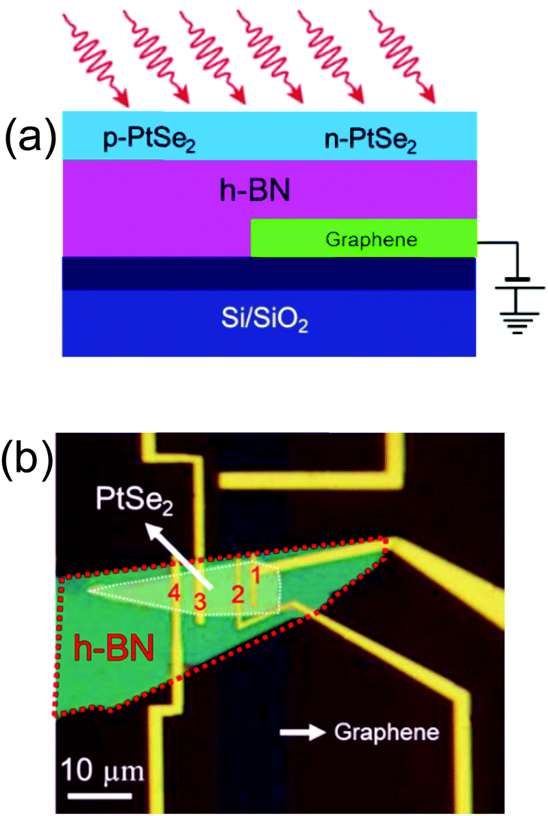 | ||
| Fig. 1 (a) Schematic design of the PtSe2/BN/Gr heterostructure on a Si/SiO2 substrate. (b) An optical image of the device showing the formation of a lateral PtSe2 p–n junction. | ||
Initially, without any doping effect the (Ids–Vds) characteristics of the PtSe2/BN/graphene van der Waals heterostructure were investigated thoroughly at back gate voltage (Vbg = 0 V) between probes (2, 3), as shown in Fig. 1a. As shown in Fig. S2 (ESI†), the device shows ohmic contact behavior. When the transport curve (Ids–Vbg) of PtSe2 was measured either between probes (1, 2) or (3, 4), it retains its original p-type conduction, as shown in Fig. S2 (ESI†). The PtSe2 nanoflake reveals a transition from a semimetal to a semiconductor as the thickness is modulated.16 Here, p-type conduction was investigated in thin PtSe2 nanoflakes (Fig. S3a, ESI†). In previous reports, devices based on thin PtSe2 nanoflakes or thin films revealed various intrinsic semiconducting properties.16,33–35 When the PtSe2/BN/graphene heterostructure was illuminated with visible light under a negative photo-induced gate voltage (−Vlightgr) of −15 V for 5 minutes the on-current in the electron regime was strongly increased, which shows carrier type variation in the PtSe2 nanoflake. Moreover, for the electron regime, the on-current nearly approaches a similar level to that of the hole regime, demonstrating a more symmetric and ambipolar type in the PtSe2 nanoflake (Fig. S3b, ESI†). At a greater value of −Vlightgr (i.e., −30 V), the electron current is further enhanced, representing an electron dominant effect (Fig. S3c, ESI†). After the doping process, the (Ids−Vbg) characteristics of PtSe2 were measured at Vbg = 0 V between the aforementioned probes. The device shows strong diode-like rectifying behavior, further confirming carrier inversion in the PtSe2 nanoflake (Fig. S2, ESI†). The mechanism of carrier modulation in the PtSe2 nanoflake under −Vlightgr is similar to the doping effect in graphene/BN heterostructures.36,37 In our case, taking advantage of −Vlightgr to graphene, the carrier type variation that occurred in the area of the PtSe2 nanoflake partially positioned on the BN/graphene heterostructure is inverted to n-type as a result of the excitation of the mid-gap states in the BN flake, while the remaining area exhibited p-type conduction (Fig. 2a). Upon illumination, the electrons are excited from mid-gap point defects in BN into its conduction band (Fig. S4, ESI†). The photoexcited electrons enter into PtSe2 under −Vlightgr, which was applied to graphene during the implementation of light (Fig. S4, ESI†). Fig. 2b displays a schematic diagram of the device structure of the PtSe2/BN/Gr heterostructure under light illumination with the implementation of −Vlightgr aimed at a photo doping effect. It can be seen from Fig. 2c that after the photo-induced effect, positive defects (or charges) remain in BN after eliminating the effect of both −Vlightgr and light illumination. Fig. S5b (ESI†) shows that after the doping process the forward and backward transfer curves represent the weak hysteresis of the device, which is comparable to the pristine device because there is no trapping of charges at the surface of BN (Fig. S5a, ESI†). Moreover, this indicates that the positive charges close to the PtSe2 channel are nearly eliminated after 5 minutes of the photo doping process, and also this further supports our conclusion that the positively charged defects are deep in the BN flake.
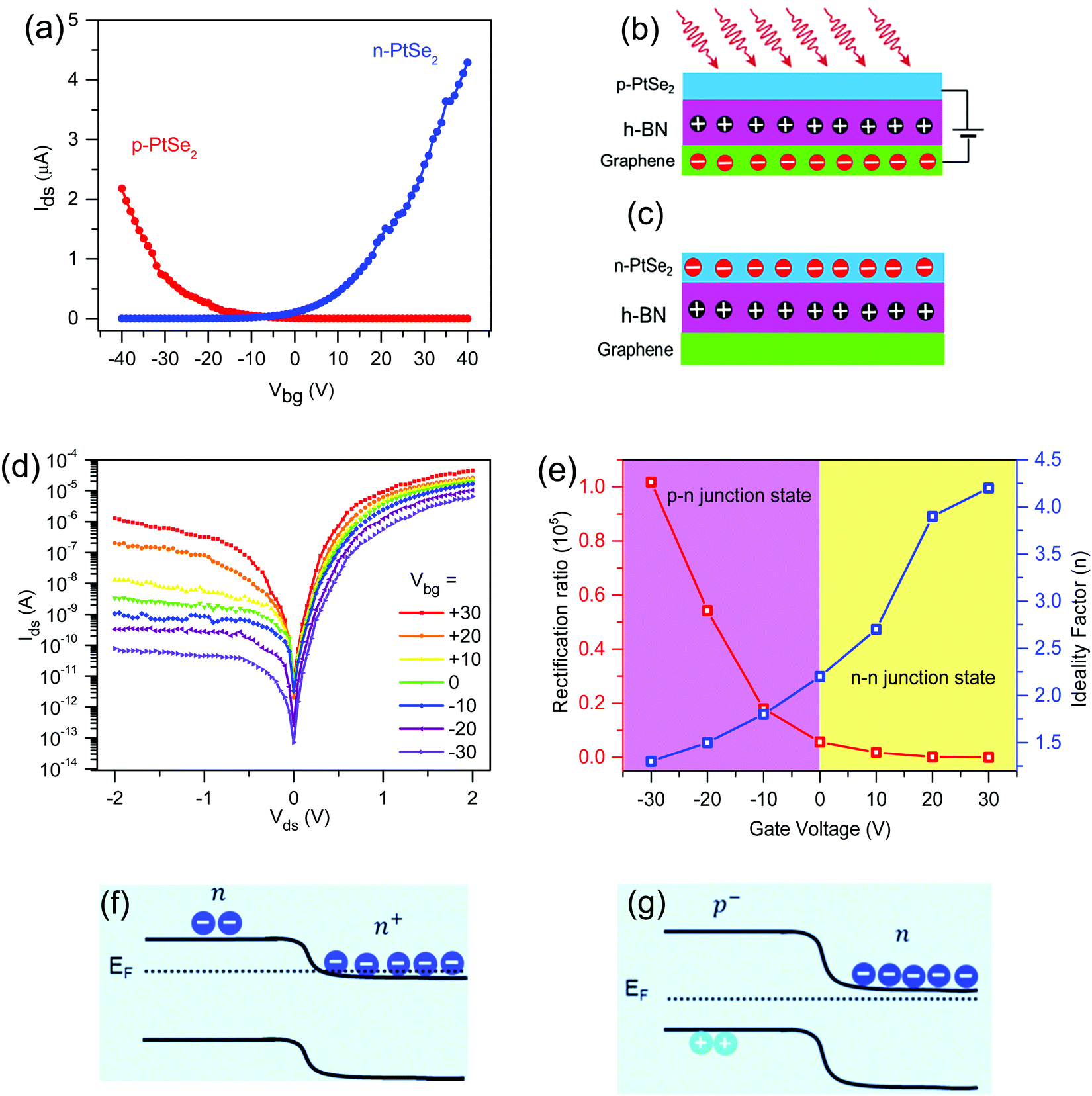 | ||
| Fig. 2 (a) Transfer curves (Ids–Vbg) of p-PtSe2 and n-PtSe2 at Vds = 1 V. Representation of the PtSe2/BN/Gr van der Waals heterostructure (b) under light illumination with the implementation of negative gate voltage and (c) after the photo-induced effect. (d) The (Ids–Vbg)characteristics of PtSe2 p–n diodes on a log scale at different Vbg. (e) The rectification ratio and ideality factor as a function of Vbg. Schematic of the energy band diagram showing the (f) n–n+ and (g) p–n junction states. | ||
Many previous reports have described chemical p-type doping in MoS2 with AuCl3 to invert its polarity to go from n- to p-type FETs,27,38 the electrostatic gating effect for modulation of the carrier type in WSe2, and39 elemental n-type doping in BP with Al to invert its polarity to go from p- to n-type FETs.40 In the abovementioned approaches, stability of the treated devices over a long period in an ambient environment could not be guaranteed.26,27,29 Through the implementation of a photo-induced doping technique, no breakdown in the transfer characteristics was observed after keeping the devices for a long retention time. PtSe2 flakes show a steady n-type electron doping effect in air (Fig. S6a, ESI†). Moreover, the electron concentration n(n-PtSe2) in the PtSe2 flake can be described as follows:41
| n(n-PtSe2) = −Cg (Vbg − Vth)/e, | (1) |
 | (2) |
 corresponds to the length/width of the PtSe2 flake (2/6),
  represents the slope of the linear plot from the transfer curve. For example, the μ(n-PtSe2) FET was valued to be ∼9.7 cm2 V−1 s−1, e.g., at −40 V and for 0 days. Both n(n-PtSe2) and μ(n-PtSe2) as a function of retention time (in Fig. S6b, ESI†) showed almost n-type stable doping effect in PtSe2 over a long period. Moreover, we also observed stability in the rectifying behavior of the diode in an ambient environment over a long period (Fig. S7, ESI†).
In our case, the thin PtSe2 flakes have a bandgap of 0.21 eV and a work function of 4.62 eV.18 Since Ni has a work function of ∼5.2 eV, which is slightly deeper than the valence band maximum of PtSe2, it makes ohmic contact to p-type PtSe2, as shown in Fig. S8a (ESI†). Moreover, we observed the ohmic contribution of Ni contacts to n-type PtSe2 flakes by observing the linear (Ids–Vbg) characteristics, as shown in Fig. S8b (ESI†). According to the Schottky–Mott rule, the Schottky barrier height (ΦB) is related to the difference between the work function of a metal and electron affinity of a semiconductor: ΦB = Φmetal − χsemi. Nevertheless, some semiconductors do not comply with this rule due to the formation of metal-induced gap states,44–46 which fill with electrons and accordingly pin the center of the bandgap closer to the Fermi level. This influence is well known as Fermi-level pinning.47 We believe that for the above-mentioned reason the Ni/Au metals contacts may exhibit a strong ohmic contribution to PtSe2. A further reason is that for thin 2D nanoflakes the metals electrodes diffuse into them which results in a low Schottky barrier or ohmic contribution.48–50
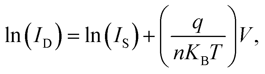
The lateral PtSe2 diode rectifying behavior was estimated at different gate bias (Vbg) from (−30 to +30 V) with a step of 10 V as shown in Fig. 2d. The PtSe2 diode exhibits minor diode-like behavior from 0 to +30 V. As Vbg changes from −10 to −30 V, the junction current promptly declines in the reverse bias regime as compared to the forward bias. In Fig. 2e, a greater change in the rectification ratio, i.e., forward bias to reverse bias currents , at a constant Vds value of ±2 V can be observed. The diode shows a rectification ratio of up to ∼1.0 × 10⁵ (Fig. 2e). The lateral PtSe2 diode shows a better rectification ratio in contrast to those reported in previous studies.28,51–55 The rectifying behavior of the PtSe2 p–n diode initiates from the amendment of the built-in potential at the junction of p-PtSe2 and n-PtSe2 by variation in Vds as a function of gate voltage. As Vbg changes from 0 to +30 V, the n−n+ junction state exists as a result of the movement of the Fermi level (EF) close to the conduction band of p-PtSe2 and n-PtSe2 where the electrons become dominant in both of the channels, as shown in the band profile of Fig. 2f. Instead, as the Vbg changes from 0 to −30 V, the Fermi level moves near to the bandgap of p-PtSe2 and n-PtSe2 and consequently a p–n junction state (in Fig. 2g) occurs owing to the formation of built-in potential at the homointerface, causing a superior change in the rectification ratio. Fig. 2e shows the variation in the rectification ratio of the PtSe2 homojunction p–n diode, which changes from ∼0.68 × 101 to ∼1.0 × 10⁵ when the gate voltage varies from −30 to +30 V. Furthermore, the ideality factor can be determined in the forward-biased regime using the interpretation form of the diode equation:25,41,43
 | (3) |
Under laser irradiation, the PtSe2 homojunction p–n diode can separate the photoexcited charge carriers to advance the photonic devices. Our diode exhibits the p–n junction state under dark conditions at Vbg = 0 V. Fig. 3a shows the (Ids–Vds) characteristics of the attained diode in both the dark and upon the illumination of light (λ = 600 nm) with various intensities of laser light. It can be seen that a self-biased phenomenon exists upon the illumination of incident light, and a positive open-circuit voltage (Voc = 0.32 V) is created, i.e., the voltage obtained at zero current and also a negative short-circuit current (Isc = 16.2 nA) is produced, the current obtained at zero voltage bias, showing the distinctive self-biased photovoltaic behavior of the PtSe2 homojunction p–n diode. Fig. 3b shows the electrical power (Pele.) as a function of the operating voltage at various intensities of laser irradiation, which is obtained from the product of Ids and Vds. The PtSe2 homojunction p–n diode can operate as a photovoltaic device, i.e., it can generate a maximum electrical power of 1.87 nW at Vds = 225 mV for 40 mW cm−2 intensity of incident light. Using laser light with a greater intensity can generate more electron–hole pairs, causing the (Ids–Vds) curves to shift towards more negative values of the short circuit current, as shown in Fig. 3a, and the value of the electrical power also increases (Fig. 3b). Furthermore, the values of Isc and Voc are linearly reliant on the intensity of the laser light (Fig. 3c), which is comparable to previous reports.56,57 A self-biased photoresponse of the PtSe2 homojunction p–n diode was observed at a different intensity of incident light, as shown in Fig. 4a. It is clear that as the power of laser irradiation increased from 8 to 40 mW cm−2 the photocurrent (Iph = Iillumination − Idark) improved from 8.3 to 14.4 nA. Furthermore, as shown in Fig. 4b, as the wavelength changes from 200 to 1200 nm (40 mW cm−2), the photocurrent decreases from 22.09 to 0.8 nA. We calculated the photoresponsivity (R) and the detectivity (d) using the following equations: R = Jp/Pin, D = R/Jd, where Jp and Pin are the photocurrent density and input power, respectively, and Jd is the dark current density. Our device shows a maximum high responsivity of 1487.9 mA W−1 and a detectivity of 2.0 × 10⁹ Jones with a power intensity of 8 mW cm−2 (λ = 600 nm) for a junction area of 112 μm2. Fig. 4c shows the relationship between the responsively and detectivity as a function of the incident light intensity. The external quantum efficiency (EQE) can be found using the following equation:58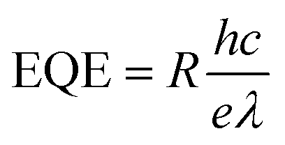 , where Iph represents the photocurrent, PLaser represents the laser power, λ = 600 nm represents the wavelength of light illumination, c represents the speed of light, and h represents Planck's constant.25,43 We measured the EQE of the device at zero gate bias, which gave a value of 3068%, greater than the values previously reported.59,60 The better photovoltaic performance of our PtSe2 homojunction p–n diode could be due to the continuous bandaging of the p-PtSe2 and n-PtSe2 junctions with small-bandgap materials. Fig. 4d shows the EQE as a function of light intensity. Fig. 4e shows the relationship between the normalized photocurrent to dark current ratio (NPDR) and noise equivalent power (NEP), which can be estimated using the following equations NPDR = R/Id,
  where R, Id, and q represent the responsivity, the dark current, and electronic charge, respectively. The values of NPDR and NEP were calculated to be 1.2 × 10⁹ w−1 and 0.41 × 10⁻¹² W Hz−1/2, respectively. The NEP value reveals that the PtSe2 p–n diode is capable of sensing power in the picowatt range, which is essential for photovoltaic devices that are used in disaster applications. The rise and fall time were estimated using the equations:61
 respectively, where A and B are constants and λ1 and (λ2) are the rise and decay time constants. Subsequently, through the fitting of these equations, we estimated a rise time of 31 ms and a fall time of 33 ms. Fig. 5a shows an illustration of the PtSe2 based p–n diode showing its mechanism as a switching photodiode. The maximum value of the open-circuit voltage (Voc = 0.35 V) is achieved (as an output) directly as the incident light is switched on (as an input) and quickly disappears when the light is switched off, showing switching behavior of the PtSe2 p–n diode state upon the switching on and off of light (40 mW cm−2), as shown in Fig. 5b. Besides a homojunction p–n diode, homogeneous PtSe2 as an inverter was also achieved via carrier type variation in the PtSe2 channel using this elegant photodoping technique. The inset of Fig. 5c shows a diagram of the PtSe2 homoinverter in which the two channels are connected in series. Upon the illumination of light, the two FET channels can be doped selectively. One FET channel demonstrates n-type transport conduction after the use of the photoinduced doping technique, whereas the remaining one preserves its original p-type transport behavior. Three metal electrodes were deposited on PtSe2 nanoflake consecutively to work as the VDD, Vout, and GND, which represent the power supply, output signal, and ground, respectively. The input signal (Vin) was supplied to the graphene underneath BN, which also serves as a bottom gate electrode. The output characteristics (Vin–Vout) of the PtSe2 homoinverter with a sweep of the input signal from −2 to +2 V are shown in Fig. 5c. To determine the performance of the PtSe2 homoinverter, the gain
  was extracted from the slope of the (Vin–Vout) curve. Finally, this elegant photodoping technique was used to form homoinverters with a gain of almost ∼30 at VDD = 2 V, as shown in Fig. 5c, which showed better performance than in previous reports. The stable doping effect in 2D PtSe2 offers an easy way to develop NMD-based photovoltaic and complementary nano-electronic devices.
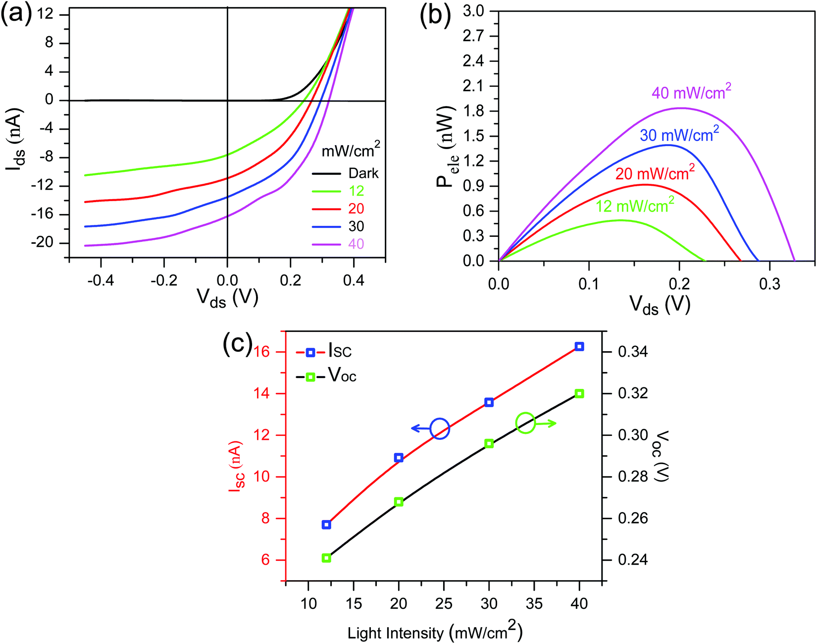 | ||
| Fig. 3 (a) The (Ids–Vbg)characteristics of PtSe2 homojunction p–n diodes in the dark and the upon illumination of light with different intensities (λ = 600 nm). (b) The electrical power of PtSe2 homojunction p–n diodes at different light intensities. (c) Self-biased created Voc and Isc as a function of light intensity. | ||
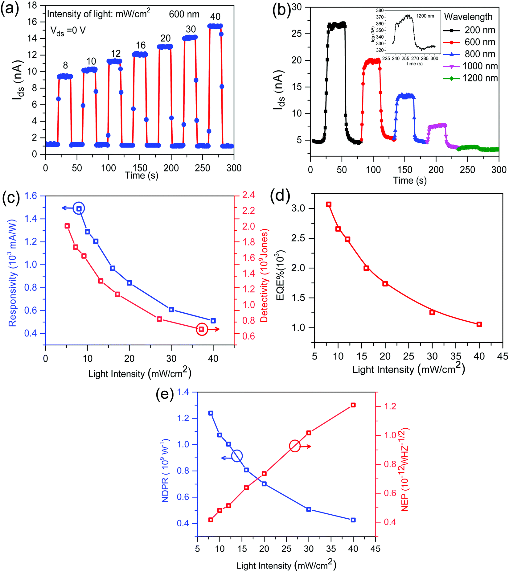 | ||
| Fig. 4 (a) Photoresponse of the p–n junction under the illumination of various intensities of light (λ = 600 nm) at Vds = 0 V. (b) Photoresponse of the p–n junction under the illumination of different wavelengths of incident light (40 mW cm−2). The inset of b shows the enlarged photoresponse at 1200 nm. (c) Responsivity (mA W−1) and detectivity (Jones), (d) EQE, and (e) normalized photocurrent to dark current ratio NPDR (W−1) and noise equivalent power NEP (W Hz−1/2) as a function of the intensity of light. | ||
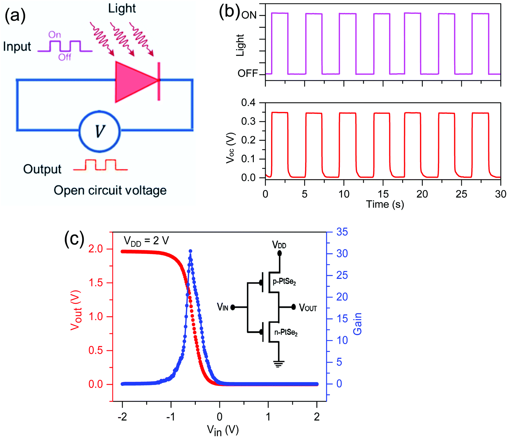 | ||
| Fig. 5 (a) An illustration of a PtSe2 based p–n diode showing its mechanism as a switching photodiode. (b) Voc switching behavior in the p–n diode state upon the switching on and off of light (40 mW cm−2). (c) Output characteristics of p- and n-type PtSe2 FET based inverters with extracted gains of the inverter as a function of the input voltage. The inset in c shows a diagram of a homoinverter based on PtSe2. | ||
4. Conclusion
In summary, novel lateral PtSe2 p–n diodes were demonstrated based on a PtSe2/BN/graphene van der Waals heterostructure upon the illumination of visible light via the optical excitation of mid-gap donor-like states in boron nitride. A stable photodoping effect was achieved for inverting the polarity of aPtSe2 based FET from the p- to n-type. The PtSe2 p–n diodes exhibit rectifying performance, with a rectification ratio of up to ∼1.0 × 10⁵ and an ideality factor of ∼1.3. The devices show good self-biased photovoltaic behavior upon laser irradiation and also show Voc switching behavior in the p–n diode state upon the switching on and off of light. They also exhibit a broadband photoresponse over a wavelength range from 200 to 1200 nm and various photovoltaic parameters were examined. Also, p-PtSe2 and n-PtSe2 FETs were used to fabricate a homoinverter that reach a maximum gain of ∼30 (VDD = 2 V). The work in this study can aid in the development of the application of 2D NMDs in future electronics and complementary electronic devices.Conflicts of interest
The authors declare no competing financial interests.Acknowledgements
This work is funded by the Higher Education Commission (HEC) of Pakistan under the National Research Program for Universities (NRPU) with project no. HEC/R&D/NRPU/2017/7876 and 5544/KPK/NRPU/R&D/HEC/2016.References
- S. Aftab, M. F. Khan, K.-A. Min, G. Nazir, A. M. Afzal, G. Dastgeer, I. Akhtar, Y. Seo, S. Hong and J. Eom, Nanotechnology, 2017, 29, 045201 CrossRef.
- O. Lopez-Sanchez, D. Lembke, M. Kayci, A. Radenovic and A. Kis, Nat. Nanotechnol., 2013, 8, 497–501 CrossRef CAS.
- C. Lan, C. Li, Y. Yin and Y. Liu, Nanoscale, 2015, 7, 5974–5980 RSC.
- N. Perea-López, A. L. Elías, A. Berkdemir, A. Castro-Beltran, H. R. Gutiérrez, S. Feng, R. Lv, T. Hayashi, F. López-Urías and S. Ghosh, Adv. Funct. Mater., 2013, 23, 5511–5517 CrossRef.
- X. Qiu, Y. Huang, Z. Nie, B. Ma, Y. Tan, Z. Wu, N. Zhang and X. Xie, Nanoscale, 2020, 12, 1109–1117 RSC.
- S. Aftab, Ms. Samiya, S. Yousuf, M. U. Khan, R. Khawar, A. Younus, M. Manzoor, M. W. Iqbal and M. Z. Iqbal, Nanoscale, 2020, 12, 15687–15696 RSC.
- P. T. K. Loan, W. Zhang, C. T. Lin, K. H. Wei, L. J. Li and C. H. Chen, Adv. Mater., 2014, 26, 4838–4844 CrossRef CAS.
- D. Kong, H. Wang, J. J. Cha, M. Pasta, K. J. Koski, J. Yao and Y. Cui, Nano Lett., 2013, 13, 1341–1347 CrossRef CAS.
- J. Klinovaja and D. Loss, Phys. Rev. B: Condens. Matter Mater. Phys., 2013, 88, 075404 CrossRef.
- S. Aftab, Ms. Samiya, H. M. Ul Haq, S. Yousuf, M. U. Khan, Z. Ahmed, M. W. Iqbal, A. ur Rehman and M. Z. Iqbal, Adv. Mater. Interfaces, 2020, 202001479 Search PubMed.
- T. Georgiou, R. Jalil, B. D. Belle, L. Britnell, R. V. Gorbachev, S. V. Morozov, Y.-J. Kim, A. Gholinia, S. J. Haigh and O. Makarovsky, Nat. Nanotechnol., 2013, 8, 100–103 CrossRef CAS.
- M. W. Iqbal, K. Shahzad, G. Hussain, M. K. Arshad, R. Akbar, S. Azam, S. Aftab, T. Alharbi and A. Majid, Mater. Res. Express, 2019, 6, 115909 CrossRef CAS.
- M. W. Iqbal, E. Elahi, A. Amin, S. Aftab, I. Aslam, G. Hussain and M. A. Shehzad, Superlattices Microstruct., 2020, 147, 106698 CrossRef CAS.
- S. Rehman, M. F. Khan, S. Aftab, H. Kim, J. Eom and D.-k. Kim, J. Mater. Chem. C, 2019, 7, 725–732 RSC.
- Y. Zhao, J. Qiao, Z. Yu, P. Yu, K. Xu, S. P. Lau, W. Zhou, Z. Liu, X. Wang and W. Ji, Adv. Mater., 2017, 29, 1604230 CrossRef.
- A. Ciarrocchi, A. Avsar, D. Ovchinnikov and A. Kis, Nat. Commun., 2018, 9, 1–6 CrossRef CAS.
- M. Ghorbani-Asl, A. Kuc, P. Miró and T. Heine, Adv. Mater., 2016, 28, 853–856 CrossRef CAS.
- S. Sattar and U. Schwingenschlogl, ACS Appl. Mater. Interfaces, 2017, 9, 15809–15813 CrossRef CAS.
- W. L. Chow, P. Yu, F. Liu, J. Hong, X. Wang, Q. Zeng, C. H. Hsu, C. Zhu, J. Zhou and X. Wang, Adv. Mater., 2017, 29, 1602969 CrossRef.
- M. Tosun, S. Chuang, H. Fang, A. B. Sachid, M. Hettick, Y. Lin, Y. Zeng and A. Javey, ACS Nano, 2014, 8, 4948–4953 CrossRef CAS.
- Z. Hu, Z. Wu, C. Han, J. He, Z. Ni and W. Chen, Chem. Soc. Rev., 2018, 47, 3100–3128 RSC.
- W. Luo, M. Zhu, G. Peng, X. Zheng, F. Miao, S. Bai, X. A. Zhang and S. Qin, Adv. Funct. Mater., 2018, 28, 1704539 CrossRef.
- W. Liao, L. Wang, L. Chen, W. Wei, Z. Zeng, X. Feng, L. Huang, W. C. Tan, X. Huang and K. W. Ang, Nanoscale, 2018, 10, 17007–17014 RSC.
- S. Fan, X. Tang, D. Zhang, X. Hu, J. Liu, L. Yang and J. Su, Nanoscale, 2019, 11, 15359–15366 RSC.
- S. Aftab, M. Samiya, M. W. Iqbal, P. Shinde, M. F. Khan, A. ur Rehman, S. Yousaf, S. Park and S. C. Jun, Nanoscale, 2020, 12, 18171–18179 RSC.
- H. Fang, M. Tosun, G. Seol, T. C. Chang, K. Takei, J. Guo and A. Javey, Nano Lett., 2013, 13, 1991–1995 CrossRef CAS.
- X. Liu, D. Qu, J. Ryu, F. Ahmed, Z. Yang, D. Lee and W. J. Yoo, Adv. Mater., 2016, 28, 2345–2351 CrossRef CAS.
- M. S. Choi, D. Qu, D. Lee, X. Liu, K. Watanabe, T. Taniguchi and W. J. Yoo, ACS Nano, 2014, 8, 9332–9340 CrossRef CAS.
- B. Chen, H. Sahin, A. Suslu, L. Ding, M. I. Bertoni, F. Peeters and S. Tongay, ACS Nano, 2015, 9, 5326–5332 CrossRef CAS.
- N. Ubrig, S. Jo, H. Berger, A. F. Morpurgo and A. B. Kuzmenko, Appl. Phys. Lett., 2014, 104, 171112 CrossRef.
- Y. Zhang, J. Ye, Y. Yomogida, T. Takenobu and Y. Iwasa, Nano Lett., 2013, 13, 3023–3028 CrossRef CAS.
- L. Ju, J. Velasco, E. Huang, S. Kahn, C. Nosiglia, H.-Z. Tsai, W. Yang, T. Taniguchi, K. Watanabe and Y. Zhang, Nat. Nanotechnol., 2014, 9, 348–352 CrossRef CAS.
- C. Yim, K. Lee, N. McEvoy, M. O’Brien, S. Riazimehr, N. C. Berner, C. P. Cullen, J. Kotakoski, J. C. Meyer and M. C. Lemme, ACS Nano, 2016, 10, 9550–9558 CrossRef CAS.
- X. Yu, P. Yu, D. Wu, B. Singh, Q. Zeng, H. Lin, W. Zhou, J. Lin, K. Suenaga and Z. Liu, Nat. Commun., 2018, 9, 1–9 CrossRef.
- C. Yim, N. McEvoy, S. Riazimehr, D. S. Schneider, F. Gity, S. Monaghan, P. K. Hurley, M. C. Lemme and G. S. Duesberg, Nano Lett., 2018, 18, 1794–1800 CrossRef CAS.
- C. R. Dean, A. F. Young, I. Meric, C. Lee, L. Wang, S. Sorgenfrei, K. Watanabe, T. Taniguchi, P. Kim and K. L. Shepard, Nat. Nanotechnol., 2010, 5, 722 CrossRef CAS.
- P. Zomer, S. Dash, N. Tombros and B. Van Wees, Appl. Phys. Lett., 2011, 99, 232104 CrossRef.
- X. Liu, Y. Yuan, D. Qu and J. Sun, Phys. Status Solidi RRL, 2019, 13, 1900208 CrossRef.
- R. Frisenda, A. J. Molina-Mendoza, T. Mueller, A. Castellanos-Gomez and H. S. van der Zant, Chem. Soc. Rev., 2018, 47, 3339–3358 RSC.
- Y. Liu, Y. Cai, G. Zhang, Y. W. Zhang and K. W. Ang, Adv. Funct. Mater., 2017, 27, 1604638 CrossRef.
- S. Aftab, I. Akhtar, Y. Seo and J. Eom, ACS Appl. Mater. Interfaces, 2020, 12, 42007–42015 CrossRef CAS.
- J. Wang, F. Ma and M. Sun, RSC Adv., 2017, 7, 16801–16822 RSC.
- S. Aftab, M. W. Iqbal, A. M. Afzal, M. F. Khan, G. Hussain, H. S. Waheed and M. A. Kamran, RSC Adv., 2019, 9, 10017–10023 RSC.
- K.-A. Min, J. Park, R. M. Wallace, K. Cho and S. Hong, 2D Mater., 2016, 4, 015019 CrossRef.
- S. Picozzi, A. Continenza, G. Satta, S. Massidda and A. Freeman, Phys. Rev. B: Condens. Matter Mater. Phys., 2000, 61, 16736 CrossRef CAS.
- S. Aftab and J. Eom, 2D Mater., 2019, 6, 035005 CrossRef.
- C. Kim, I. Moon, D. Lee, M. S. Choi, F. Ahmed, S. Nam, Y. Cho, H.-J. Shin, S. Park and W. J. Yoo, ACS Nano, 2017, 11, 1588–1596 CrossRef CAS.
- S. Walia, S. Balendhran, Y. Wang, R. Ab Kadir, A. Sabirin Zoolfakar, P. Atkin, J. Zhen Ou, S. Sriram, K. Kalantar-Zadeh and M. Bhaskaran, Appl. Phys. Lett., 2013, 103, 232105 CrossRef.
- H. Liu, M. Si, Y. Deng, A. T. Neal, Y. Du, S. Najmaei, P. M. Ajayan, J. Lou and P. D. Ye, ACS Nano, 2014, 8, 1031–1038 CrossRef CAS.
- J. Kang, W. Liu and K. Banerjee, Appl. Phys. Lett., 2014, 104, 093106 CrossRef.
- T. Liu, D. Xiang, Y. Zheng, Y. Wang, X. Wang, L. Wang, J. He, L. Liu and W. Chen, Adv. Mater., 2018, 30, 1804470 CrossRef.
- J. S. Ross, P. Klement, A. M. Jones, N. J. Ghimire, J. Yan, D. Mandrus, T. Taniguchi, K. Watanabe, K. Kitamura and W. Yao, Nat. Nanotechnol., 2014, 9, 268 CrossRef CAS.
- A. Pospischil, M. M. Furchi and T. Mueller, Nat. Nanotechnol., 2014, 9, 257–261 CrossRef CAS.
- D. J. Groenendijk, M. Buscema, G. A. Steele, S. Michaelis de Vasconcellos, R. Bratschitsch, H. S. van der Zant and A. Castellanos-Gomez, Nano Lett., 2014, 14, 5846–5852 CrossRef CAS.
- M. Buscema, D. J. Groenendijk, G. A. Steele, H. S. Van Der Zant and A. Castellanos-Gomez, Nat. Commun., 2014, 5, 1–6 Search PubMed.
- Y. Deng, Z. Luo, N. J. Conrad, H. Liu, Y. Gong, S. Najmaei, P. M. Ajayan, J. Lou, X. Xu and P. D. Ye, ACS Nano, 2014, 8, 8292–8299 CrossRef CAS.
- Y. Jin, D. H. Keum, S. J. An, J. Kim, H. S. Lee and Y. H. Lee, Adv. Mater., 2015, 27, 5534–5540 CrossRef CAS.
- S. Aftab, M. F. Khan, P. Gautam, H. Noh and J. Eom, Nanoscale, 2019, 11, 9518–9525 RSC.
- M. M. Furchi, A. Pospischil, F. Libisch, J. Burgdörfer and T. Mueller, Nano Lett., 2014, 14, 4785–4791 CrossRef CAS.
- P. Chen, T. T. Zhang, J. Xiang, H. Yu, S. Wu, X. Lu, G. Wang, F. Wen, Z. Liu and R. Yang, Nanoscale, 2016, 8, 3254–3258 RSC.
Footnote |
| † Electronic supplementary information (ESI) available. See DOI: 10.1039/d0tc04642f |
| This journal is © The Royal Society of Chemistry 2021 |