
Resistive switching in formamidinium lead iodide perovskite nanocrystals: a contradiction to the bulk form†
Chinnadurai
Muthu
ab,
A. N.
Resmi
c,
Johnpaul K.
Pious
ab,
G.
Dayal
c,
Nayana
Krishna
a,
K. B.
Jinesh
 *c and
C.
Vijayakumar
*ab
*c and
C.
Vijayakumar
*ab
aPhotosciences and Photonics Section, CSIR-National Institute for Interdisciplinary Science and Technology (NIIST), Thiruvananthapuram 695 019, India. E-mail: cvijayakumar@niist.res.in
bAcademy of Scientific and Innovative Research (AcSIR), Ghaziabad 201 001, India
cDepartment of Physics, Indian Institute of Space Science and Technology (IIST), Thiruvananthapuram 695 547, India. E-mail: kbjinesh@iist.ac.in
First published on 17th November 2020
Abstract
Hybrid perovskites have emerged as an excellent class of materials for resistive random access memory (ReRAM) devices and neuromorphic computing applications. Among numerous perovskites, formamidinium lead triiodide (α-FAPbI3) is an important material due to its superior optoelectronic properties. However, it does not show resistive switching due to the difficulties in rupturing the filaments formed by iodide vacancies. Herein, we report the ReRAM device characteristics of α-FAPbI3 in the nanocrystal form, prepared in a single-step method. Unlike the bulk form, the nanocrystals show reliable, and reproducible memory characteristics in terms of program/erase operations, data retention, and endurance with an operating set voltage of around 2 V. Our studies revealed that the iodide vacancies are responsible for the switching and the presence of capping ligands plays a significant role in it. The capping ligands reduce the interaction energy between the iodide vacancies, and hence the filaments formed by the latter are easy to rupture during the reset process resulting in excellent ReRAM characteristics.
Introduction
Memory devices are essential components in modern electronic devices for data storage and processing. Advancement in information technology necessitates further improvements of these devices in various aspects such as storage density, switching speed, and power consumption.1 In this context, resistive random access memory (ReRAM) devices have emerged as a promising candidate due to their smaller size, simple device architecture, low-switching voltage, high storage density, fast switching, scalability, and low cost of fabrication.2–7 Importantly, they exhibit non-volatile nature as the stored data could be maintained even without the power supply.8 The resistive switching of ReRAM devices is usually caused by the formation and breakage of conducting filaments/channels or charge trapping by defect sites.9–11 Semiconductors such as inorganic perovskites, metal oxides, organic, and two-dimensional materials are widely used in ReRAM devices.12–18 Among them, inorganic perovskites are of great interest, but the high-temperature processability and brittle nature are the major drawbacks of these materials.19–21Recently, organic–inorganic halide perovskites or hybrid perovskites were found to be suitable for ReRAM application as they exhibit good charge carrier transport assisted by defects.22–25 The first report on a hybrid perovskite-based memory device was made by Wang et al. using the bulk form of CH3NH3PbI3−xClx.23 Though the device operated at low switching voltages, thick films (2.5 μm) were required to avoid the pin-holes. Subsequently, we reported CH3NH3PbBr3 nanocrystal based devices with excellent bipolar resistive switching behavior and remarkable stability under ambient conditions.26 The thickness of the active layer was only about 200 nm because the presence of capping ligands in the nanocrystals facilitates the formation of high quality, pin-hole-free films. We have also illustrated the tuning of the switching parameters through chloride doping to the perovskite structure. The write-erase voltages of the devices were reduced with increasing chloride content while the on/off ratio, endurance, and retention were increased. Later, various groups have reported perovskite-based memory devices with improved properties.27–32 Recent developments in this area suggest that hybrid perovskites are attractive candidates for neuromorphic computing applications, which implies their great potential.33–35
Alpha formamidinium lead triiodide, α-HC(NH2)2PbI3 (α-FAPbI3), is an important material among many hybrid perovskites due to its superior optical and electronic properties.36–38 Park et al. have studied the ReRAM behavior of this perovskite in the bulk form.39 They observed that the material was inactive in ReRAM devices due to the difficulties in the rupturing of the conducting channels formed by the iodide vacancies (VI). Density Functional Theory (DFT) calculations revealed that the electronic states of VI are overlapped with and diffused through the conduction band. As a result, two VI interact through the conduction band, and the increase in physical distance does not decrease the interaction energy between them. Therefore, the formed VI channels at the set process are tough to rupture during the reset process. We hypothesized that the use of α-FAPbI3 in the nanocrystal form would solve this issue since the presence of capping ligands in the nanocrystals may reduce the interaction energy between VI and thus facilitate the rupture of the conductive channels formed by them during the reset process. To prove our hypothesize, we studied the resistive switching properties of α-FAPbI3 in the nanocrystal form. The fabricated ReRAM devices using a thin layer of nanocrystals showed stable and reproducible bipolar resistive switching properties. They also showed excellent memory device characteristics such as low-voltage operation, long-term data retention, and high endurance.
Results and discussion
α-FAPbI3 perovskite nanocrystals (PNCs) are usually prepared via a two-step hot injection method, which involves the synthesis of highly moisture-sensitive formamidinium oleate precursor.40,41 In the present work, we synthesized these nanocrystals by a simple single-step process without the synthesis of formamidinium oleate. Briefly, formamidinium iodide in the dimethylformamide–oleic acid mixture was injected into a solution containing 1-octadecene, lead iodide, oleic acid, and oleylamine at 80 °C. The obtained nanocrystals were washed with toluene and characterized using a transmission electron microscope (TEM) and X-ray diffraction (XRD) spectrometer. TEM analysis showed that the nanocrystals were rectangular with an average edge length of 9.3 nm (Fig. 1a and Fig. S1, ESI†). The XRD profile showed peaks corresponding to (001), (011), (111), (002), (012), (112), (022), and (003) planes (Fig. 1b), indicating the cubic structure of the nanocrystals.42 The XRD spectrum also confirmed both the chemical purity (absence of peaks corresponding to lead iodide) and phase purity (absence of δ-phase) of PNCs. The phase purity was further confirmed from XPS analysis (Fig. S2, ESI†).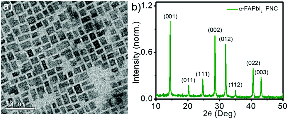 | ||
| Fig. 1 (a) TEM image of α-FAPbI3 PNCs drop cast from toluene solution onto the carbon-coated Cu grid. (b) The XRD pattern of the PNC film coated on a glass substrate. | ||
For fabricating memory devices, PNCs were dispersed in toluene via probe sonication for 30 minutes and spin-coated on an FTO-glass substrate to get a uniform and smooth film with a thickness of around 200 nm. After drying the film under ambient conditions, a 200 nm thick aluminum (Al) layer was thermally evaporated onto the film to obtain memory devices with a structure of FTO/PNC/Al. The area of an individual device was 1 mm2. The schematic representation and the cross-sectional scanning electron microscope (SEM) images of the device are shown in Fig. 2a and b, respectively. The uniformity of the PNC film on the FTO substrate was evident from the SEM image. Smoothness of the film and the absence of pin-holes were confirmed from topological SEM and AFM images (Fig. S3, ESI†). The current–voltage (I–V) sweeping of the ReRAM device is shown in Fig. 2c. As the bias voltage increased to 2.3 V, the device initially at the low resistance state (LRS) was switched to the high resistance state (HRS, reset process). The device remained in the HRS until applying a negative reverse bias voltage. The switching back to the LRS was observed at −2.4 V (set process). The devices were tested with larger voltage sweeps, but no unipolar switching behavior was observed (Fig. S4, ESI†). The occurrence of set and reset processes at opposite bias polarities indicates a bipolar resistive switching property of the device. The reliability of the devices was confirmed from Weibull distributions of the set and reset voltages measured from 25 devices (Fig. 2d).
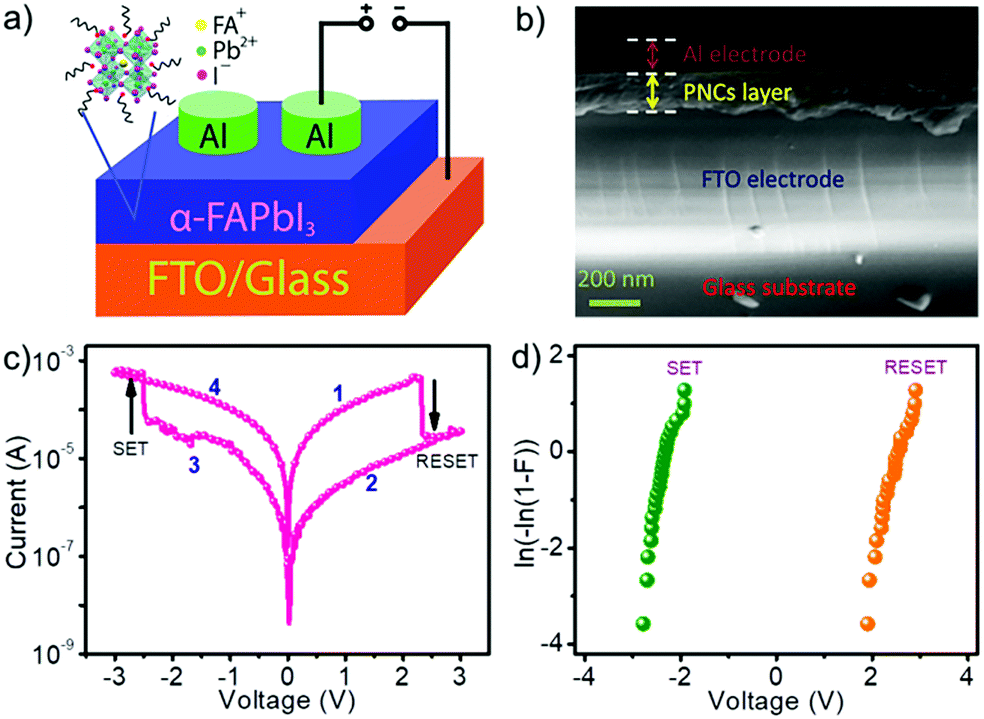 | ||
| Fig. 2 (a) Schematic diagram and (b) cross-sectional SEM image of the memory device fabricated from PNCs. (c) Typical current–voltage (I–V) characteristics of a memory device. (d) The plot of Weibull distributions of the set and reset voltages obtained from 25 devices. | ||
The device was initially in the LRS instead of HRS, contrary to the observation in most bulk perovskite-based memory devices.27–32 This observation implies that the PNCs don’t need any electroforming process, and the conducting path is already available without any externally applied voltage. To get a plausible explanation for this observation, X-ray photoelectron spectroscopy (XPS) analysis of the PNC film was carried out. The XPS spectrum of Pb 4f showed two intense peaks at 138.2 and 143.2 eV corresponding to Pb2+ and two low-intensity peaks at 136.3 and 141.1 eV, indicating the presence of metallic Pb (Fig. 3). During purification of PNCs, VI may be generated due to the partial detachment of the capping ligands.43–45 These vacancies can trigger a redox reaction reducing the interstitial Pb2+ to metallic Pb. This process is known as ‘valence change’46 and is responsible for observing XPS peaks corresponding to the metallic Pb. An underlying implication of this observation confirms the presence of VI in the PNC film. In other words, the observed peaks in XPS indicate not only the presence of metallic Pb but also the VI, which is attributed to the initial LRS of the device. Though metallic Pb is present in the film, the formation and rupturing of the conducting channels are exclusively caused by VI because Pb is difficult to move. During the reset process, the self-formed conducting channels are broken due to the movement of VI to the bottom electrode. A schematic diagram illustrating the set and reset processes are shown in Fig. S5 (ESI†).
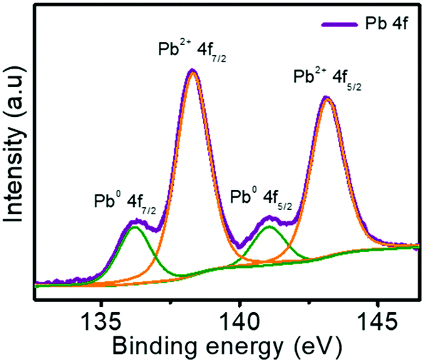 | ||
| Fig. 3 Pb 4f XPS spectra of PNC film on an FTO substrate. | ||
Since aluminum was used as the top electrode, arguably, there is one more possibility for switching; aluminum is known for the interfacial oxidation (Fig. S6, ESI†) and has been reported to be one reason for resistive switching.47,48 In this type of switching, the device will be in the ON state initially and go to an OFF state on applying the electric field. To rule out the possibility of the aluminum electrode contribution to resistive switching, memory devices with gold as the top electrode were fabricated and characterized (device structure: FTO/PNCs/Au). Typical I–V characteristics of such a device are shown in Fig. S7 (ESI†), which was similar to that of the aluminum-based devices. This observation confirmed that the aluminum electrode has no role in the resistive switching property of PNCs. Another aspect to rule out is the possibility of the origin of the memory effect due to the phase change between perovskite/non-perovskite phases. Certain perovskites in the bulk form known to exhibit switching between perovskite/non-perovskite phases and are used to develop memory devices.49 However, the perovskite material used in the present case is in the form of nanocrystals with hydrophobic capping ligands. They are highly stable and do not undergo phase changes, as evident from the absorption and XRD spectra (Fig. S8, ESI†). To prove that there is no phase change during the switching of the device from LRS to HRS, we have analyzed the XPS profile of the material in the HRS state (Fig. S9, ESI†). The XPS profile remained exactly similar to that of the LRS state, which excluded the possibility of the phase change based resistive switching mechanism.
The conduction mechanism was investigated by plotting natural logarithmic I–V plots corresponding to the SET and RESET processes (Fig. 4). In the SET process, the slopes of HRS at low (green line) and high (blue line) electric fields were different. The slope of ∼1 at the low electric field indicates Ohmic conduction. On the other hand, the slope of ∼2.7 observed at a high electric field indicates space charge limited current (SCLC) conduction with some contributions from the Poole–Frenkel conduction mechanism. Poole–Frenkel charge injection is a trap-assisted conduction mechanism, where the electrons get emitted from traps into the conduction band of the dielectric by thermal excitation. The linear relationship between ln(J/E) and E1/2, where J is current density and E is the electric field, is a proof for this mechanism (Fig. S10, ESI†). This situation remains the same until the applied reverse voltage reaches near −2.4 V, where the SET process occurs. At this point, the current abruptly increased, and the slope changed into Ohmic (green line), resulting in the formation of conducting channels. In the RESET process, the slope of LRS (green line) represents Ohmic conduction, which is in agreement with the LRS mechanism in the SET process. When the applied voltage is near 2.3 V, a sudden decrease in current occurs, and the device switches to HRS due to the disruption of the conducting channels, again following Ohmic conduction. This analysis revealed that the involved conduction mechanisms are Ohmic, SCLC, and Poole–Frenkel. All of them come under the bulk-limited conduction mechanisms, which depends on the electrical properties of the dielectric (PNC film) itself and rules out the contribution from the electrode assisted interface switching mechanism.46,50,51 The R2 values or the ‘coefficient of determination’ for all carrier transport sections were calculated using linear fitting and indicated in the inset of Fig. 4. Excellent fitting values (99.9%) were obtained for the LRS section because the current flows without any fluctuations through well-defined conducting filaments formed by the close vicinity of VI. On the other hand, no such filaments are available in the HRS, and fluctuations in current flow are possible due to the apparent charge trapping and de-trapping in various trap states.52,53 As a result, the R-squared values were slightly lower (99.4–99.7%) than the ideal numbers.
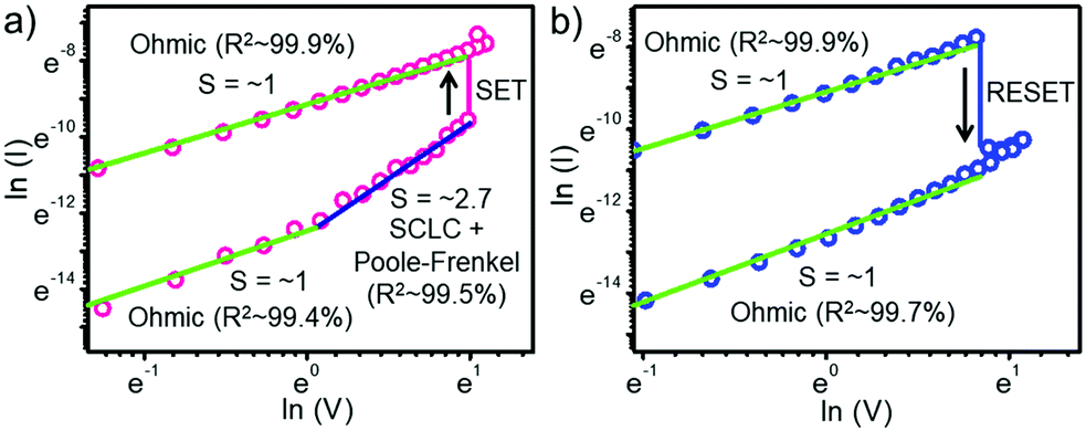 | ||
| Fig. 4 Natural logarithmic I–V plots corresponding to the (a) SET and (b) RESET processes of a typical memory device. The slopes of the plots and the conduction mechanisms are indicated inside the graphs. The R-squared values for the linear fitting for each carrier transport sections are also indicated. | ||
To demonstrate the potential of the material as a rewritable resistive switching memory device, write–read–erase–read cycling tests (endurance) were carried out. In this experiment, DC voltage pulses were applied consecutively to evaluate the electrical stability at VSET = −3 V and VRESET = 3 V. The reading voltage of the device was fixed at 1 V. The endurance was tested for 1200 cycles, and the device exhibited stable switching throughout the experiment. The first 75 cycles of the endurance analysis are shown in Fig. 5a. The complete set of endurance cycling data is given in the supporting information (Fig. S11, ESI†). The retention performance of the device at room temperature was measured for 1000 s (Fig. 5b). The on- and off-states were measured at an applied voltage of 1 V at ambient temperature. Though the HRS was stable throughout the experiment, the LRS current was found to be decreasing. Bulk switching materials such as metal oxides exhibit similar behavior, mainly due to the filament structure relaxation phenomenon.54–57 It is known that the diffusion of VI is facile in lead halide perovskites under an applied voltage due to the low activation energy (∼0.60 eV).58,59 The migration of VI from the conducting filaments would reduce its diameter leading to the reduction of current flow. Such a process is possible in the present devices also, and should be responsible for the observed decrease in the LRS current.
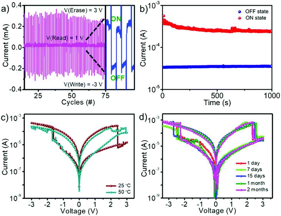 | ||
| Fig. 5 (a) 75 cycles of the endurance analysis of the devices (writing voltage: −3 V, erasing voltage: 3 V, reading voltage: 1 V). Zoomed area of three cycles shown on the right side. (b) LRS and HRS as a function of retention time measured at 1 V. The current–voltage characteristics of a memory device measured at different (c) temperatures and (d) time. | ||
The stability of the device was monitored at two different temperatures (25 °C and 50 °C) (Fig. 5c). It is observed that the LRS to HRS transition occurs at a slightly earlier voltage, and the off-current after setting to HRS is larger at increased temperatures. This observation indicates that the initial LRS is due to the aggregation of mobile hopping sites, where the temperature assists the diffusion of the iodide vacancies. For any practical applications, devices should be stable for an extended period. Most of the hybrid lead halide perovskite materials are unstable under ambient conditions and require an inert atmosphere for the fabrication and storage of devices. Metal oxides were used as the protective layer for the long-term stability of methylammonium/cesium lead halide perovskite based memory devices.60 On the other hand, the PNCs used in this work are highly stable for several months without using any external layer. As a result, they showed similar resistive switching properties even after two months (Fig. 5d).
As mentioned earlier, α-FAPbI3 perovskite in the bulk form was inactive in the ReRAM devices due to the difficulty in the rupturing of the conducting channels formed by VI.39 On the other hand, PNCs exhibited excellent resistive switching behavior. A significant difference between the bulk and nanocrystal forms is the presence of capping ligands in the latter. The large bandgap, electronically inactive capping ligands such as oleylammonium and oleate ions used in the present case attached to the surface, could act as an energy barrier between the adjacent nanocrystals (Fig. S12, ESI†). In other words, the capping ligands reduce the overlapping of energy levels between the neighboring nanocrystals.61–65 Consequently, though it is difficult to calculate, it could be assumed that the interaction energy between the VI present in adjacent PNCs will be lowered. As a result, it was possible to rupture the VI channels formed during the reset process resulting in ReRAM characteristics. The switching parameters are excellent and on par with many of the hybrid perovskites with a comparable device architecture (Table S1, ESI†). In addition to that, contrary to the bulk state, the nanocrystal form of α-FAPbI3 has excellent phase retention behavior and high moisture tolerance making them suitable for real-world applications.
Conclusions
In conclusion, black phase α-FAPbI3 PNCs were prepared by a simple single-step method using hydrophobic oleylammonium and oleate ions as the capping ligands. Unlike the bulk form, the memory devices fabricated with PNCs showed stable, reproducible bipolar resistive switching properties. The switching is purely related to the intrinsic property of PNCs due to the presence of halide vacancies and does not require any metal filament formation. The devices showed excellent characteristics such as low-operational voltage and longer retention time. The devices have high thermal and environmental stability for a long time.Conflicts of interest
There are no conflicts to declare.Acknowledgements
C. M. and J. K. P. are grateful to CSIR and UGC for the respective research fellowships. C. V. thanks the DST-AISRF project for partial financial support.Notes and references
- S. T. Han, Y. Zhou and V. A. L. Roy, Adv. Mater., 2013, 25, 5425–5449 CrossRef CAS.
- F. Pan, S. Gao, C. Chen, C. Song and F. Zeng, Mater. Sci. Eng., R, 2014, 83, 1–59 CrossRef.
- D. B. Strukov, G. S. Snider, D. R. Stewart and R. S. Williams, Nature, 2008, 453, 80–83 CrossRef CAS.
- J. J. Yang, D. B. Strukov and D. R. Stewart, Nat. Nanotechnol., 2012, 8, 13–24 CrossRef.
- W. Hu, L. Zou, X. Chen, N. Qin, S. Li and D. Bao, ACS Appl. Mater. Interfaces, 2014, 6, 5012–5017 CrossRef CAS.
- R. Waser and M. Aono, Nat. Mater., 2007, 6, 833–840 CrossRef CAS.
- X. Zhao, J. Ma, X. Xiao, Q. Liu, L. Shao, D. Chen, S. Liu, J. Niu, X. Zhang and Y. Wang, et al. , Adv. Mater., 2018, 14, 1705193 CrossRef.
- K. Yang, F. Li, C. P. Veeramalai and T. Guo, Appl. Phys. Lett., 2017, 110, 083102 CrossRef.
- X. Zhu, J. Lee and W. D. Lu, Adv. Mater., 2017, 29, 1700527 CrossRef.
- J.-Y. Seo, J. Choi, H.-S. Kim, J. Kim, J.-M. Yang, C. Cuhadar, J. S. Han, S.-J. Kim, D. Lee, H. W. Jang and N.-G. Park, Nanoscale, 2017, 9, 15278–15285 RSC.
- J. Ouyang, C. W. Chu, C. R. Szmanda, L. P. Ma and Y. Yang, Nat. Mater., 2004, 3, 918–922 CrossRef CAS.
- M. Prezioso, F. Merrikh-Bayat, B. Hoskins, G. Adam, K. K. Likharev and D. B. Strukov, Nature, 2015, 521, 61–64 CrossRef CAS.
- H. Y. Jeong, J. Y. Kim, J. W. Kim, J. O. Hwang, J. E. Kim, J. Y. Lee, T. H. Yoon, B. J. Cho, S. O. Kim, R. S. Ruoff and S. Y. Choi, Nano Lett., 2010, 10, 4381–4386 CrossRef CAS.
- L. Liang, K. Li, C. Xiao, S. Fan, J. Liu, W. Zhang, W. Xu, W. Tong, J. Liao, Y. Zhou, B. Ye and Y. Xie, J. Am. Chem. Soc., 2015, 137, 3102–3108 CrossRef CAS.
- Z. B. Yan and J. M. Liu, Ann. Phys., 2015, 358, 206–224 CAS.
- T. Sekitani, T. Yokota, U. Zschieschang, H. Klauk, S. Bauer, K. Takeuchi, M. Takamiya, T. Sakurai and T. Someya, Science, 2009, 326, 1516–1519 CrossRef CAS.
- X. F. Cheng, X. Hou, W. H. Qian, J. H. He, Q. F. Xu, H. Li, N. J. Li, D. Y. Chen and J. M. Lu, ACS Appl. Mater. Interfaces, 2017, 9, 27847–27852 CrossRef CAS.
- T. Roy, M. Tosun, J. S. Kang, A. B. Sachid, S. B. Desai, M. Hettick, C. C. Hu and A. Javey, ACS Nano, 2014, 8, 6259–6264 CrossRef CAS.
- W.-J. Yin, B. Weng, J. Ge, Q. Sun, Z. Li and Y. Yan, Energy Environ. Sci., 2019, 12, 442–462 RSC.
- A. Kumar, A. Kumar and V. Krishnan, ACS Catal., 2020, 10, 10253–10315 CrossRef CAS.
- W. Gao, Y. Zhu, Y. Wang, G. Yuan and J.-M. Liu, J. Materiomics, 2020, 6, 1–16 CrossRef.
- Z. Xu, Z. Liu, Y. Huang, G. Zheng, Q. Chen and H. Zhou, J. Mater. Chem. C, 2017, 5, 5810–5817 RSC.
- E. J. Yoo, M. Lyu, J.-H. Yun, C. J. Kang, Y. J. Choi and L. Wang, Adv. Mater., 2015, 27, 6170–6175 CrossRef CAS.
- H. Kim, J. S. Han, S. G. Kim, S. Y. Kim and H. W. Jang, J. Mater. Chem. C, 2019, 7, 5226–5234 RSC.
- Y. Wang, Z. Lv, L. Zhou, X. Chen, J. Chen, Y. Zhou, V. A. L. Roy and S.-T. Han, J. Mater. Chem. C, 2018, 6, 1600–1617 RSC.
- C. Muthu, S. Agarwal, A. Vijayan, P. Hazra, K. B. Jinesh and V. C. Nair, Adv. Mater. Interfaces, 2016, 3, 1600092 CrossRef.
- J. Choi, S. Park, J. Lee, K. Hong, D.-H. Kim, C. W. Moon, G. D. Park, J. Suh, J. Hwang, S. Y. Kim, H. S. Jung, N.-G. Park, S. Han, K. T. Nam and H. W. Jang, Adv. Mater., 2016, 28, 6562–6567 CrossRef CAS.
- K. Yan, B. Chen, H. Hu, S. Chen, B. Dong, X. Gao, X. Xiao, J. Zhou and D. Zou, Adv. Electron. Mater., 2016, 2, 1600160 CrossRef.
- J.-Y. Chen, Y.-C. Chiu, Y.-T. Li, C.-C. Chueh and W.-C. Chen, Adv. Mater., 2017, 29, 1702217 CrossRef.
- J.-Y. Seo, J. Choi, H.-S. Kim, J. Kim, J.-M. Yang, C. Cuhadar, J. S. Han, S.-J. Kim, D. Lee, H. W. Jang and N.-G. Park, Nanoscale, 2017, 9, 15278–15285 RSC.
- Z. Hong, J. Zhao, K. Huang, B. Cheng, Y. Xiaoa and S. Lei, J. Mater. Chem. C, 2019, 7, 4259–4266 RSC.
- F. Zhou, Y. Liu, X. Shen, M. Wang, F. Yuan and Y. Chai, Adv. Funct. Mater., 2018, 28, 1800080 CrossRef.
- H. Tian, L. Zhao, X. Wang, Y.-W. Yeh, N. Yao, B. P. Rand and T.-L. Ren, ACS Nano, 2017, 11, 12247–12256 CrossRef CAS.
- T. Mazur, P. Zawal and K. Szaciłowski, Nanoscale, 2019, 11, 1080–1090 RSC.
- R. A. John, N. Yantara, Y. F. Ng, G. Narasimman, E. Mosconi, D. Meggiolaro, M. R. Kulkarni, P. K. Gopalakrishnan, C. A. Nguyen, F. D. Angelis, S. G. Mhaisalkar, M. A. Basu and N. Mathews, Adv. Mater., 2018, 30, 1805454 CrossRef.
- G. E. Eperon, S. D. Stranks, C. Menelaou, M. B. Johnston, L. M. Herz and H. J. Snaith, Energy Environ. Sci., 2014, 7, 982–988 RSC.
- N. Pellet, P. Gao, G. Gregori, T. Y. Yang, M. K. Nazeeruddin, J. Maier and M. Grätzel, Angew. Chem., Int. Ed., 2014, 53, 3151–3157 CrossRef CAS.
- J.-W. Lee, S. H. Lee, H.-S. Ko, J. Kwon, J. H. Park, S. M. Kang, N. Ahn, M. Choi, J. K. Kim and N.-G. Park, J. Mater. Chem. A, 2015, 3, 9179–9186 RSC.
- J.-M. Yang, S.-G. Kim, J.-Y. Seo, C. Cuhadar, D.-Y. Son, D. Lee and N.-G. Park, Adv. Electron. Mater., 2018, 4, 1800190 CrossRef.
- L. Protesescu, S. Yakunin, S. Kumar, J. Bär, F. Bertolotti, N. Masciocchi, A. Guagliardi, M. Grotevent, I. Shorubalko, M. I. Bodnarchuk, C.-J. Shih and M. V. Kovalenko, ACS Nano, 2017, 11, 3119–3134 CrossRef CAS.
- P. Papagiorgis, A. Manoli, L. Protesescu, C. Achilleos, M. Violaris, K. Nicolaides, T. Trypiniotis, M. I. Bodnarchuk, M. V. Kovalenko, A. Othonos and G. Itskos, ACS Photonics, 2018, 5, 907–917 CrossRef CAS.
- H.-H. Fang, L. Protesescu, D. M. Balazs, S. Adjokatse, M. V. Kovalenko and M. A. Loi, Small, 2017, 13, 1700673 CrossRef.
- Q. A. Akkerman, G. Rainò, M. V. Kovalenko and L. Manna, Nat. Mater., 2018, 17, 394–405 CrossRef CAS.
- P. Liu, W. Chen, W. Wang, B. Xu, D. Wu, J. Hao, W. Cao, F. Fang, Y. Li, Y. Zeng, R. Pan, S. Chen, W. Cao, X. W. Sun and K. Wang, Chem. Mater., 2017, 29, 5168–5173 CrossRef CAS.
- A. Pan, J. Wang, M. J. Jurow, M. Jia, Y. Liu, Y. Wu, Y. Zhang, L. He and Y. Liu, Chem. Mater., 2018, 30, 2771–2780 CrossRef CAS.
- J.-M. Yang, E.-S. Choi, S.-Y. Kim, J.-H. Kim, J.-H. Park and N.-G. Park, Nanoscale, 2019, 11, 6453–6461 RSC.
- S. Z. Rahaman and S. Maikap, Nanoscale Res. Lett., 2013, 8, 509 CrossRef.
- V. J. Manjunath, A. Rush, A. Barua and R. Jha, Solid State Electron. Lett., 2019, 1, 52–57 CrossRef.
- C. Zou, J. Zheng, C. Chang, A. Majumdar and L. Y. Lin, Adv. Opt. Mater., 2019, 7, 1900558 CrossRef.
- F.-C. Chiu, Adv. Mater. Sci. Eng., 2014, 578168 Search PubMed.
- D. J. Kim, Y. J. Tak, W.-G. Kim, J. K. Kim, J. H. Kim and H. J. Kim, Adv. Mater. Interfaces, 2017, 4, 1601035 CrossRef.
- B. Hwang, C. Gu, D. Lee and J.-S. Lee, Sci. Rep., 2017, 7, 43794 CrossRef.
- M. Sasaki, J. Appl. Phys., 2012, 112, 014501 CrossRef.
- Y.-F. Chang, J. A. O'Donnell, T. Acosta, R. Kotlyar, A. Chen, P. A. Quintero, N. Strutt, O. Golonzka, C. Connor and J. Hicks, 2020 IEEE International Reliability Physics Symposium (IRPS), 2020 DOI:10.1109/IRPS45951.2020.9128359.
- X. Xu, H. Lv, H. Liu, Q. Luo, T. Gong, M. Wang, G. Wang, M. Zhang, Y. Li, Q. Liu, S. Long and M. Liu, Nanoscale Res. Lett., 2015, 10, 61 CrossRef.
- A. Prakash and H. Hwang, Phys. Sci. Rev., 2016, 1, 20160010 Search PubMed.
- X. Xu, H. Lv, H. Liu, T. Gong, G. Wang, M. Zhang, Y. Li, Q. Liu, S. Long and M. Liu, IEEE Electron Device Lett., 2015, 36, 129–131 Search PubMed.
- C. Eames, J. M. Frost, P. R. F. Barnes, B. C. O’Regan, A. Walsh and M. S. Islam, Nat. Commun., 2015, 6, 7497 CrossRef CAS.
- J.-W. Lee, S.-G. Kim, J.-M. Yang, Y. Yang and N.-G. Park, APL Mater., 2019, 7, 041111 CrossRef.
- Y. Wu, Y. Wei, Y. Huang, F. Cao, D. Yu, X. Li and H. Zeng, Nano Res., 2017, 10, 1584–1594 CrossRef CAS.
- A. J. Knight and L. M. Herz, Energy Environ. Sci., 2020, 13, 2024 RSC.
- S. G. Motti, F. Krieg, A. J. Ramadan, J. B. Patel, H. J. Snaith, M. V. Kovalenko, M. B. Johnston and L. M. Herz, Adv. Funct. Mater., 2020, 30, 1909904 CrossRef CAS.
- E. T. Vickers, E. E. Enlow, W. G. Delmas, A. C. DiBenedetto, A. H. Chowdhury, B. Bahrami, B. W. Dreskin, T. A. Graham, I. N. Hernandez, S. A. Carter, S. Ghosh, Q. Qiao and J. Z. Zhang, ACS Energy Lett., 2020, 5, 817 CrossRef CAS.
- J. Dai, J. Xi, L. Li, J. Zhao, Y. Shi, W. Zhang, C. Ran, B. Jiao, X. Hou and X. Duan, et al. , Angew. Chem., Int. Ed., 2018, 57, 5754 CrossRef CAS.
- E. T. Vickers, T. A. Graham, A. H. Chowdhury, B. Bahrami, B. W. Dreskin, S. Lindley, S. B. Naghadeh, Q. Qiao and J. Z. Zhang, ACS Energy Lett., 2018, 3, 2931 CrossRef CAS.
Footnote |
| † Electronic supplementary information (ESI) available: Experimental and synthetic procedures, characterization of perovskite nanocrystals and memory devices. See DOI: 10.1039/d0tc03275a |
| This journal is © The Royal Society of Chemistry 2021 |