DOI:
10.1039/D1RA07161K
(Paper)
RSC Adv., 2021,
11, 35718-35725
Spin filtering controller induced by phase transitions in fluorographane†
Received
25th September 2021
, Accepted 26th October 2021
First published on 4th November 2021
Abstract
The electronic and transport properties of fluorographane (C2HF) nanoribbons, i.e., bare (B-C2HF) and hydrogen-passivated (H-C2HF) C2HF nanoribbons, are extensively investigated using first-principles calculations. The results indicate that edge states are present in all the B-C2HF nanoribbons, which are not allowed in the H-C2HF nanoribbons regardless of the directions. The spin splitting phenomenon of band structure only appears in the zigzag direction. This behavior mainly originates from the dehydrogenation operation, which leads to sp2 hybridization at the edge. The H-C2HF nanoribbons are semiconductors with wide band gaps. However, the band gap of B-C2HF nanoribbons is significantly reduced. Remarkably, the phase transition can be induced by the changes in the magnetic coupling at the nanoribbon edges. In addition, the B-C2HF nanoribbons along the zigzag direction show optimal conductivity, which is consistent with the band structures. Furthermore, a perfect spin filtering controller can be achieved by changing the magnetization direction of the edge C atoms. These results may serve as a useful reference for the application of C2HF nanoribbons in spintronic devices.
1. Introduction
Graphene has garnered significant interest in both scientific research and technological applications due to its unique crystal structure as well as excellent physical, electric, mechanical, and chemical properties.1 However, the gapless electronic structure and chemical inertness hinders its application in the integration of traditional electronic and optoelectronic devices. To overcome this issue, chemical functionalization has been used to adjust the physical and chemical properties of graphene.2–4 In particular, significant effort has been devoted to engineer a band gap in graphene by introducing structural defects5 or by surface functionalization with H or F atoms.6,7 After covering graphene with heteroatoms, the band gap is opened due to the transformation of sp2-hybridized carbon into sp3-hybridized carbon. In contrast to graphene, hydrogenated graphene exhibits fluorescence,8 paramagnetism,9 fast heterogeneous electron transfer,10 and tunable band gap (0–3.7 eV).11 Fluorographene also shows fluorescence and enhanced electrochemical properties.12–15 Furthermore, due to the partial similarity between hydrogen and halogen atoms, studies on fluorographane (C2HF) have been conducted recently.16–18 The difference in the electronegativity between H and F atoms causes an out-of-plane dipole moment that makes the electronic structure more complex and controllable, which has triggered extensive research enthusiasm.19–22
Although several experimental and theoretical studies have focused on the synthesis and properties of fluorographane,21,23,24 the C2HF nanoribbons have been hardly investigated.19 After the formation of one-dimensional (1D) nanoribbons, the electronic and transport properties have been tuned by altering the width, doping hetero atoms, applying external field or strain, edge modification, chemical adsorption, etc.25–27 Among them, edge modification is one of the most popular methods. This is because the basic physical properties of nanoribbons are strongly related with their edge shapes, which may induce the edge states and further result in the spin polarization. Consequently, the effect of various edge passivation states in different nanoribbons has attracted considerable research attention.28,29 For example, the sp3 hybridization on the edge atoms of zigzag silicon carbon nanoribbons after the dual-hydrogenation led to a perfect spin filtering behavior (nearly 100% spin filtering efficiency).30 The edge dehydrogenation caused a transition from antiferromagnetic (AFM) state to ferromagnetic (FM) state and effectively improved the spin filtering efficiency.31 Numerous studies have revealed the influence of edge passivation states on the electronic structure and magnetic properties of nanoribbons. However, the electronic/magnetic properties of the C2HF nanoribbons with different edge passivation states have not been investigated in detail. Therefore, in this study, a series of C2HF nanoribbons with different edge states are investigated to obtain a deeper insight into the quantum behavior of the spin-resolved transport properties. Here, the band structures and transport properties of bare or hydrogen-passivated C2HF nanoribbons with armchair and zigzag edges are presented. Our results show that the spin filtering can be controlled by changing the magnetization direction of edge C atoms. The effectiveness of this method stems from the fact that it provides an easy and precise control of spin filtering properties. Combining with the advantages of 1D nanoribbons, it is potentially useful for the transfer and treatment of information, allowing faster, low-energy operations in very small and complex devices.
2. Models and calculation methods
The geometrical optimizations were conducted using density functional theory (DFT) implemented in the Vienna ab initio simulation package (VASP).32 The projector augmented wave (PAW) method was used with a cut-off energy of 400 eV. The electronic exchange and correlation energies were described by generalized gradient approximation (GGA) of Perdew–Burke–Ernzerhof (PBE) functional.33 The atomic positions were relaxed to find the lowest energy configuration with the conjugated gradient method until the force on each atom was smaller than 0.01 eV Å−1. To isolate the interaction, a vacuum region of at least 15.0 Å was applied to separate the adjacent nanoribbons. The quantum transport code ATK34,35 was employed to study the electronic transport properties of the nanoribbons. A kinetic-energy cutoff of 75 hartree was chosen. Further, k-point sampling with 1 × 1 × 21 grid was used for the static electronic structure and band structure calculations. A double-ζ plus polarization (DZP) basis set was constructed for the H, C, and F atoms, and the same exchange–correlation functional was adopted. The C2HF nanoribbons were separated by a 25 × 35 Å vacuum slab in the x × y-plane to neglect the interactions among the periodic images.
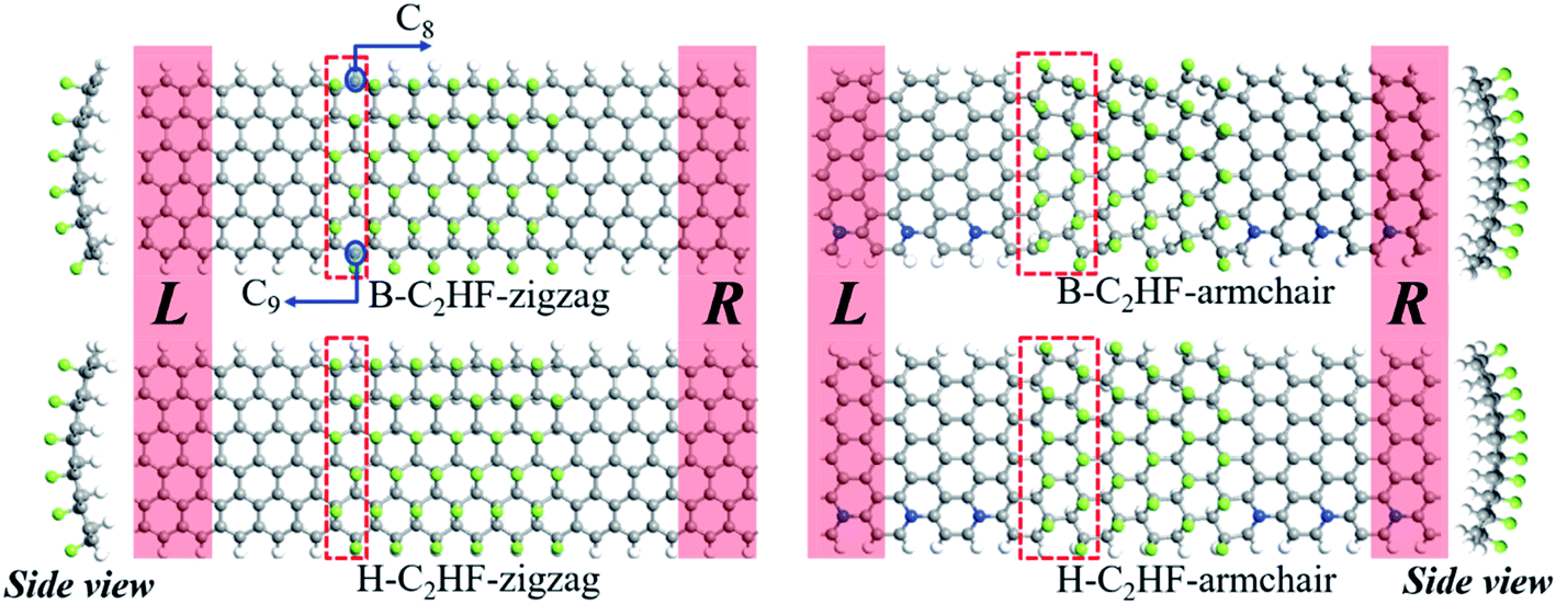
After geometrical optimization, the relaxed structure of C2HF is a puckered surface, and the perfectly planar graphene plane is locally buckled, as shown in Fig. 1. Here, C2HF nanoribbons with different edges are considered, including bare and hydrogen-passivated nanoribbons, which are abbreviated as B-C2HF and H-C2HF nanoribbons, respectively. The primitive nanoribbons cells with minimum number of atoms marked in Fig. 1 are used in the electronic structure calculations. The lengths of C–C, C–H, and C–F bonds are 1.53, 1.11, and 1.37 Å, respectively. The two-probe models are constructed for the electronic transport simulation, as depicted in Fig. 1. The graphene was selected as the electrode materials of the device along zigzag direction. Since the pristine armchair graphene nanoribbon is a semiconductor, the N-doped armchair graphene nanoribbons36 are used as electrode materials along the armchair direction. The buffer layers extending from the electrode are used to shield the interaction between the electrodes.
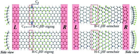 |
| | Fig. 1 Two-probe model for the electronic transport simulation of B-C2HF-zigzag, B-C2HF-armchair, H-C2HF-zigzag, and H-C2HF-armchair. The marked unit nanoribbon cells are selected as the structures for the bulk system calculations. | |
3. Results and discussions
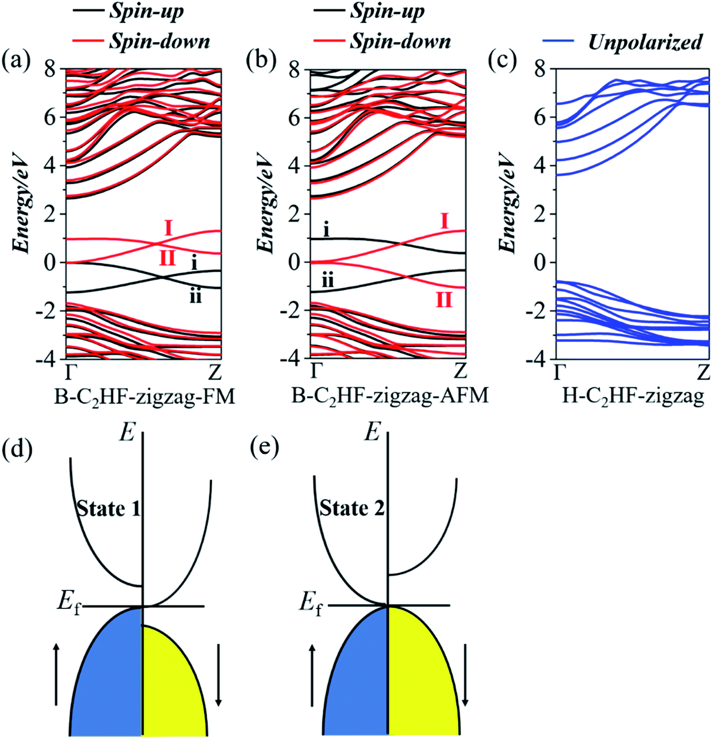
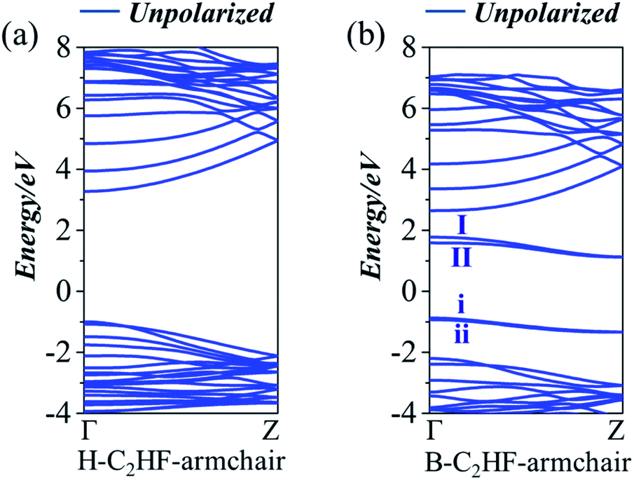
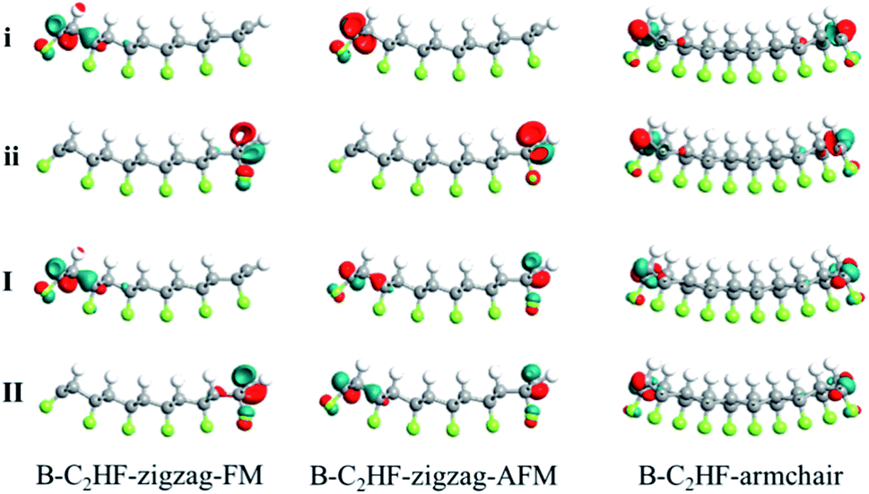
The electronic structures of the B-C2HF (H-C2HF) nanoribbons in gas phase are first investigated. It is clear from Fig. 2 and 3 that H-C2HF nanoribbons have larger band gaps than B-C2HF nanoribbons, irrespective of zigzag or armchair edges. These larger band gaps indicate that the edge hydrogen-passivated nanoribbons are electrochemically stable with poor charge transport properties. B-C2HF nanoribbons are extremely different from H-C2HF nanoribbons. Due to the dehydrogenation operation, the band gap characteristics of B-C2HF nanoribbons are similar to those of graphene nanoribbons, where the B-C2HF-zigzag nanoribbon behaves as a conductor and the B-C2HF-armchair nanoribbon behaves as a semiconductor. Thus, the reduction of the band gap in these nanoribbons can be attributed to the introduction of additional bands. As seen from the Bloch states in Fig. 4, the wave functions of these additional bands (bands I, II, i, and ii), which are called edge-related bands in B-C2HF nanoribbons, are predominantly localized on the edges. In contrast, the Bloch states of the other bands of C2HF nanoribbons are distributed at the central region of the nanoribbons, as shown in Tables S1 and S2.† Fundamentally, the dehydrogenation changes the hybridization mode of the edge C atoms from sp3 to sp2, and the original strong C–H covalent bonds break into a dangling bond, where the unpaired electrons localized on the edge C atoms increase the activity of the system and reduce the band gap. In addition, these edge-related bands show excellent dispersion characteristics, and these bands are different from the localized bands caused by impurities37,38 along the symmetry line of Γ–Z. It can be inferred that the B-C2HF nanoribbons exhibit excellent charge transport capabilities at low voltages, especially the nanoribbons with zigzag boundaries.
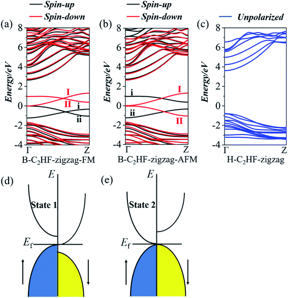 |
| | Fig. 2 (a) Band structures of B-C2HF-zigzag-FM, (b) band structures of B-C2HF-zigzag-AFM, (c) band structures of H-C2HF-zigzag nanoribbons, and (d) and (e) energy band diagrams for spin gapless semiconductors of state 1 and state 2. | |
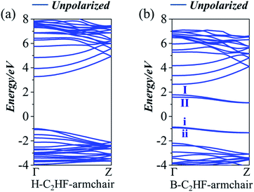 |
| | Fig. 3 Band structures of (a) H-C2HF-armchair nanoribbons, and (b) B-C2HF-armchair nanoribbons. | |
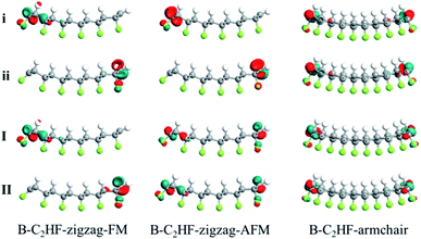 |
| | Fig. 4 Bloch states of edge-related bands at Γ for B-C2HF-zigzag-FM, B-C2HF-zigzag-AFM, and B-C2HF-armchair nanoribbons. | |
By artificially setting the spin polarizabilities (same or opposite to each other, i.e., FM and AFM state) of the C atoms at the edge of the nanoribbons to simulate an external magnetic field, an interesting phase transition phenomenon is observed in the B-C2HF-zigzag nanoribbons: a spin gapless semiconductor state 1 to a spin gapless semiconductor state 2. Although, they are all spin gapless semiconductors.39–41 But, the B-C2HF-zigzag nanoribbons with the FM state display a spin gapless semiconductor state 1 character: there is a gap between the conduction and valence bands for both the majority and minority electrons, while there is no gap between the majority electrons in the valence band and the minority electrons in the conduction band, as shown in Fig. 2d. However, that with the AFM state behave as a spin gapless semiconductor state 2 character: one spin channel is gapless, while the other spin channel is semiconducting, as shown in Fig. 2e. In other words, the features of the electronic properties can be manipulated by the magnetic field (the variation in the magnetic field indicates the variation in the magnetic coupling mode of the edge C atoms), which means that this transition is experimentally feasible. In addition, another important electronic effect: spin splitting of both AFM and FM states, is shown in Fig. 2. The difference is that both the spin-up and spin-down states show gapless properties in the FM state and the band edge touch at the Fermi level (Ef) at Γ point. However, the charge carriers in the spin-up state are mainly holes, while that in the spin-down state are primarily electrons. Interestingly, the AFM state exhibits different electronic characteristics: the spin-down state presents a gapless character, and it turns into semiconductor with a band gap of 0.72 eV in the spin-up state. The obvious spin splitting near the Ef originates from the change in the electronic configuration of edge C atoms. As mentioned above, the dehydrogenation changes the hybridization state of edge C atoms from sp3 into sp2. The unpaired electrons in the adjacent sp2-hybridized C atoms result in spin splitting. The spin polarization caused by the edge C (C8 and C9, as shown in Fig. 1) can also be seen from the magnetic moment in Table S5.† Clearly, the magnetic moment of B-C2HF-zigzag nanoribbon of both the FM and AFM state mainly arises from the C at the edge. However, a completely different spin splitting is observed in B-C2HF-armchair nanoribbon. Although such kinds of C atoms are also present in B-C2HF-armchair nanoribbon, no spin splitting happens due to the different configuration, as shown in Fig. 3b. To determine the reason for this phenomenon, we calculated the Mulliken population of BC2HF-armchair and B-C2HF-zigzag nanoribbons. Comparing with the results, it is found that the Mulliken population of the edge C atoms in B-C2HF-armchair nanoribbons is similar to that in the central region, which has sp3 hybridization, as seen in Table S3.† In this case, the electrons are paired and no unpaired electron exits. In contrast, the Mulliken population of the edge C atoms in B-C2HF-zigzag nanoribbons is special: there is almost one charge difference between spin-up and spin-down atoms, indicating the presence of unpaired electrons, as shown in Table S4.†
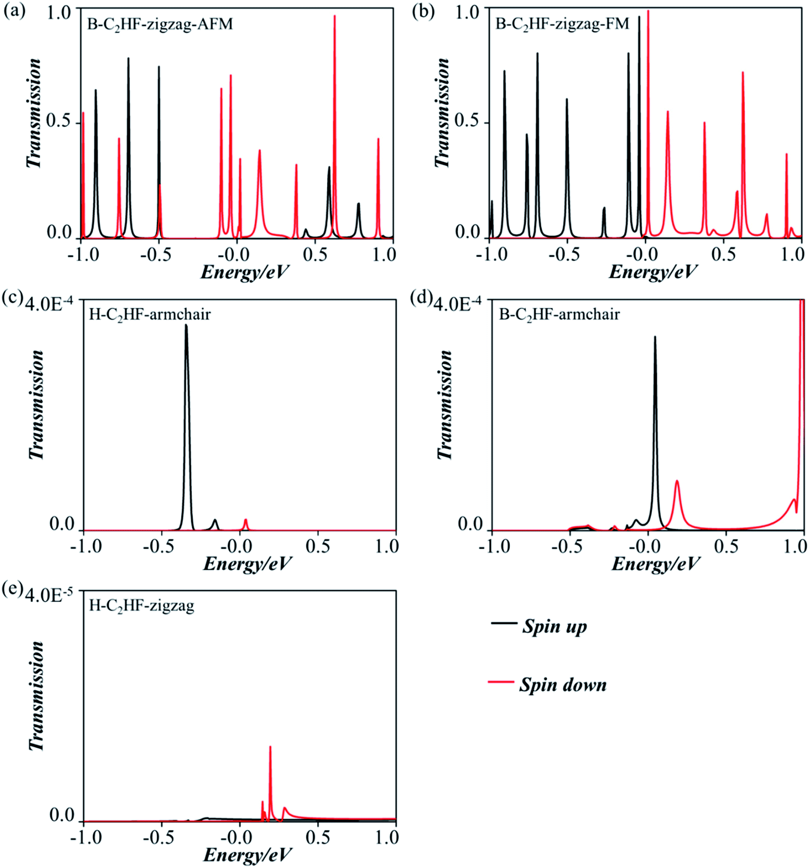
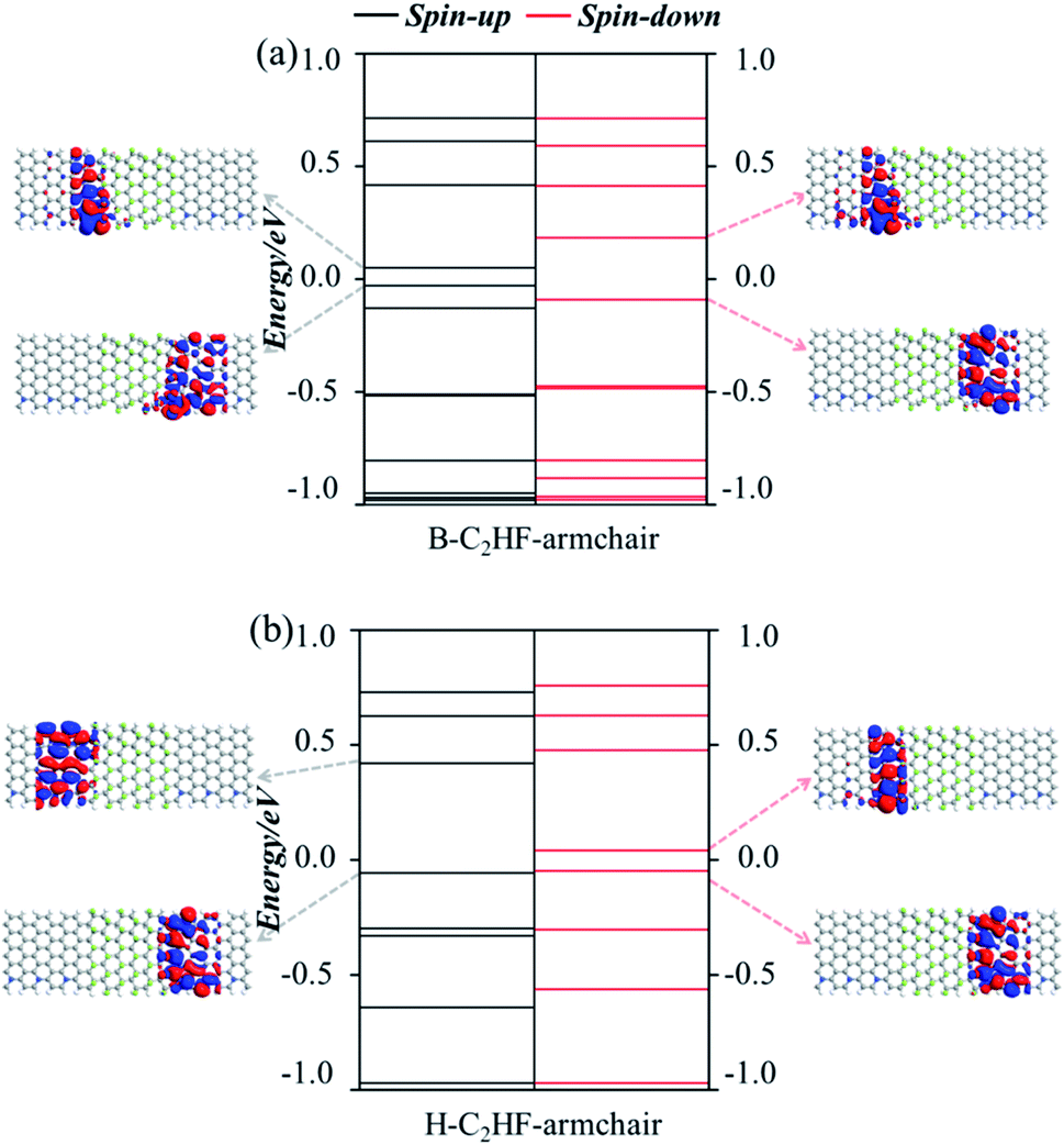
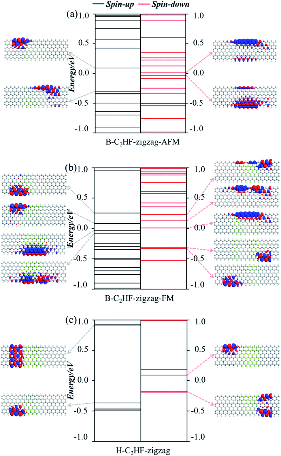
Another interesting issue is the conductive mechanism of the nanoribbons with various edges. Therefore, the transmission functions were calculated to clarify the quantum behavior and electron transmission channels. We can intuitively find that the most obvious distinction between the five transmission functions is the intensity, which can vary by four or five orders of magnitude or more (Fig. 5). From the analysis of the band structures, it is concluded that all the C2HF nanoribbons along the armchair direction have a very large band gap. After these nanoribbons are combined with the electrode material, due to the resonance between the electronic wave functions, some energy levels appear near the Ef (as shown in Fig. 6), but these energy levels are highly localized at the interface and cannot promote electron transmission. Consequently, both H-C2HF-armchair and B-C2HF-armchair nanoribbons show extremely small transmission coefficients. On the other hand, in the zigzag direction, the hydrogenation of the H-C2HF-zigzag nanoribbon causes the edge C atoms to become sp3 hybridized and the electrons are in inert state, causing the energy levels to move away from the Ef. The only few energy levels near Ef in the spin down state of the H-C2HF-zigzag nanoribbon (Fig. 7c) are also localized in the buffer layers. Correspondingly, the bare nanoribbons B-C2HF-zigzag show a large transmission value, and it originates from the active single electron in sp2 hybridization, which introduces more energy levels near Ef, as shown in Fig. 7a and b. Contrary to H-C2HF-zigzag nanoribbon, these energy levels are all completely delocalized through the scattering region. Of course, this is consistent with the band structures, i.e., B-C2HF-zigzag nanoribbon shows spin gapless semiconductor character, while H-C2HF-zigzag nanoribbon shows semiconductor characteristics with a larger band gap. From these results, it can be inferred the conductivity of B-C2HF-zigzag nanoribbon is optimal. More interestingly, the spin polarization of electrons makes the transport phenomenon more complex. Hereafter, we mainly focus on the spin-related transport of B-C2HF-zigzag nanoribbons.
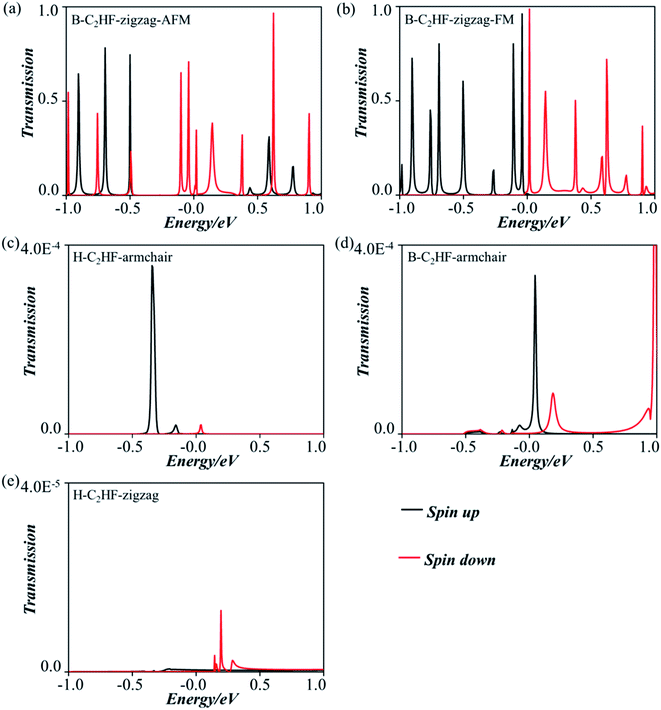 |
| | Fig. 5 Transmission spectra of (a) B-C2HF-zigzag-AFM, (b) B-C2HF-zigzag-FM, (c) H-C2HF-armchair, (d) B-C2HF-armchair, and (e) H-C2HF-zigzag nanoribbons. | |
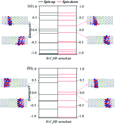 |
| | Fig. 6 Molecular energy spectra of (a) B-C2HF-armchair, and (b) H-C2HF-armchair nanoribbons. | |
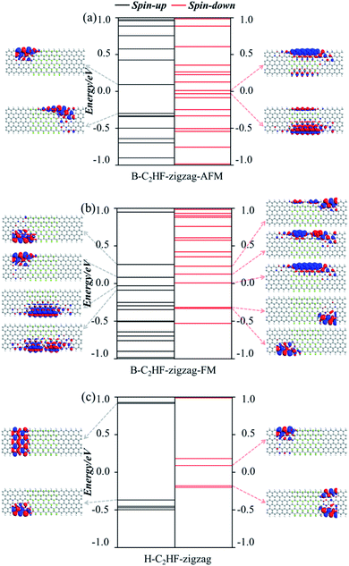 |
| | Fig. 7 Molecular energy spectra of (a) B-C2HF-zigzag-AFM, (b) B-C2HF-zigzag-FM, and (c) H-C2HF-zigzag nanoribbons. | |
Consistent with the band structures, both the AFM and FM states of the B-C2HF-zigzag nanoribbons are calculated. The conductance of both AFM and FM states is highly spin-polarized. The difference is that the frontier molecular orbitals of the AFM state are dominated almost entirely by the spin-down state, while those of the FM state are equally controlled by spin-up and spin-down states, i.e. the highest occupied molecular orbital (HOMO) is provided by the spin-up state, and the lowest unoccupied molecular orbital (LUMO) is dominated by the spin-down state. Specifically, the spin-down electronic state governs the transport in the low voltage range (when the energies of electrons are localized in the range of −0.5 to 0.5 eV) for AFM state, but that is controlled by both spin-up and spin-down for the FM state, which causes the perfect spin filtering, as shown in Fig. 5a and b. The energy level distributions and orbital wave functions in Fig. 7a can provide a deeper perspective to understand this phenomenon: the wave function distributions of frontier orbitals for the two polarization directions are completely different. For the AFM state, these spin-up orbitals are highly localized, but the spin-down orbitals exhibit excellent delocalization. The delocalization may facilitate the construction of effective electron transmission channels. However, for the FM state, taking the Ef as the dividing line, the composition of the electron transmission channels is completely different. The channels with energy above and below the Ef are independently constructed by spin-up and spin-down orbitals, respectively, as shown in Fig. 5b. This is because there are a large number of single electrons with parallel spins in the system. The Hund's rule governs the arrangement of electrons in the orbitals, i.e., each orbital must contain one electron, each spinning in the same direction, before the electrons can be paired in the orbitals. The occupation of single electrons splits the original degenerate spin orbitals, one of which is an occupied spin-up orbital, and the others are empty spin-down orbitals. The partial orbital wave functions intuitively reveal the contribution of related molecular orbitals to the electron transmission. As seen in Fig. 7b, the occupied spin-up orbitals and empty spin-down orbitals display good delocalization characteristics, which can construct effective electron transmission channels.
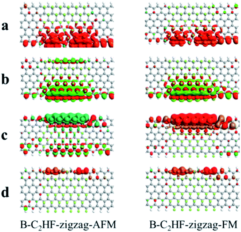
In addition, the conductance of a device is determined by the spatial distribution of the frontier molecular orbitals.42 For example, one frontier molecular orbital has a high possibility to resonate with the electronic states in the electrodes if the orbitals spread over the entire device, resulting in a more beneficial conductivity. Therefore, we calculated the eigenstates of the transmission peaks (a, b, c, and d) near the Ef. Obviously, the transmission eigenstates of a, b, c and d, which originate from the edge of nanoribbons, are delocalized across the central region and strongly coupled with two electrodes, as shown in Fig. 8, which is an essential prerequisite for the resonant transmission.
 |
| | Fig. 8 Transmission energy eigenstates corresponding to the transmission peaks near Ef of B-C2HF-zigzag nanoribbons. | |
To recapitulate, the edge states play an important role in the transport mechanism. The change in the hybridization of edge C atoms leads to spin splitting. For the FM state, the occupied spin-up orbitals and empty spin-down orbitals can all construct effective electron transmission channels. However, for the AFM state, the spin-down electronic state governs the transport in the low voltage range. Obviously, the spin-up transmission is filtered out during the transition from FM to AFM state. Therefore, we can realize a perfect spin filtering controller through switch the magnetization at any time. This effect can be achieved by changing the magnetization direction of edge C atoms, and the corresponding schematic diagram is shown in Fig. 9. Obviously, the frontier molecular orbitals of the FM state are equally controlled by spin-up and spin-down states that lead to two effective electron transmission channels. While for the AFM state, the frontier molecular orbitals are dominated almost entirely by the spin-down state which result in only one effective electron transmission channels. Compared with graphene nanoribbons, the novel B-C2HF-zigzag nanoribbons exhibit almost perfect spin current switching due to the synergistic effect between the sp2 and sp3 hybridization. In the B-C2HF-zigzag nanoribbons, the sp3 hybridization mode of the C atoms in the central region causes the system to have a large band gap. On the other hand, the sp2 hybridization originating from the dehydrogenation of edge C atoms introduces several active bands, which are gapless near Ef. In general, from the perspective of the band structures, the edge-related bands not only exhibit excellent dispersion characteristics similar to graphene nanoribbons, but also display extremely obvious spin splitting. In terms of transport, the spin transmission channels can be easily tuned from on to off state (or vice versa) by an external magnetic field under low voltage region.
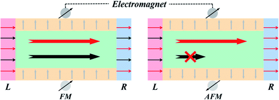 |
| | Fig. 9 Schematic diagram of the modulation of system transport properties by external magnetic field. | |
4. Conclusions
The electronic structure and transmission properties of the C2HF nanoribbons with different edges were investigated in detail through DFT theoretical calculations. The main difference between B-C2HF and H-C2HF nanoribbons was the presence of edge states in the B-C2HF nanoribbons both along the armchair and zigzag directions. In the armchair direction, the B-C2HF and H-C2HF nanoribbons were all semiconductors, and the edge states had a minor effect on the transport properties. In contrast, the edge states improved the conductivity of B-C2HF-zigzag nanoribbons. The dehydrogenation operation changed the hybridization of edge C atoms from sp3 into sp2, resulting in spin splitting. Further, the following electronic feature transition was observed: B-C2HF-zigzag nanoribbons with FM displayed a spin gapless semiconductor state 1 character, while that with AFM behaved as a spin gapless semiconductor state 2. More interestingly, the spin polarization of electrons caused the transport to become more complex in the B-C2HF-zigzag nanoribbons. With the transition from FM to AFM state, the system exhibited an obvious spin filtering effect, i.e., the spin-up transmission vanished. Therefore, a perfect spin filtering controller could be realized through the transition between FM and AFM states. Overall, our analysis can serve as practical tool for revealing the nature of the edges in realistic samples and can be used for experimentally exploring the applications of such spin filtering controllers in optoelectronic devices.
Conflicts of interest
There are no conflicts to declare.
Acknowledgements
This work was supported by the Doctoral Scientific Research Foundation of Shandong Jiaotong University (BS50004943), the Scientific Research Fund Project of Shandong Jiaotong University (Z201916 and Z201918), and National Natural Science Foundation of China (51803109 and 51973046).
References
- K. S. Novoselov, A. K. Geim, S. V. Morozov, D. Jiang, Y. Zhang, S. V. Dubonos, I. V. Grigorieva and A. A. Firsov, Science, 2004, 306, 666–669 CrossRef CAS PubMed.
- F. Obite, Nanosci. Nanotechnol., 2020, 4, 1–48 Search PubMed.
- N. Chavoshi and R. Jahanmardi, Fullerenes, Nanotubes, Carbon Nanostruct., 2019, 27, 1–9 CrossRef CAS.
- Y. Wen, E. Gao, Z. Hu, T. Xu, H. Lu, Z. Xu and C. Li, Nat. Commun., 2019, 10, 2446 CrossRef PubMed.
- P. Kot, J. Parnell, S. Habibian, C. Straßer, P. M. Ostrovsky and C. R. Ast, Phys. Rev. B, 2020, 101, 235116 CrossRef CAS.
- S. K. Achar, L. Zhang and J. K. Johnson, J. Phys. Chem. C, 2021, 125, 14874–14882 CrossRef CAS.
- A. Kouloumpis, D. D. Chronopoulos, G. Potsi, M. Pykal, J. Vlček, M. Scheibe and M. Otyepka, Chem.–Eur. J., 2020, 26, 6518–6524 CrossRef CAS PubMed.
- R. A. Schäfer, J. M. Englert, P. Wehrfritz, W. Bauer, F. Hauke, T. Seyller and A. Hirsch, Angew. Chem., Int. Ed., 2013, 52, 754–757 CrossRef PubMed.
- A. Y. S. Eng, H. L. Poh, F. Šaněk, M. Maryško, S. Matějková, Z. Sofer and M. Pumera, ACS Nano, 2013, 7, 5930–5939 CrossRef CAS PubMed.
- A. Y. Eng, Z. Sofer, P. Šimek, J. Kosina and M. Pumera, Chem.–Eur. J., 2013, 19, 15583–15592 CrossRef CAS PubMed.
- J. Sofo, A. Chaudhari and G. Barber, Phys. Rev. B: Condens. Matter Mater. Phys., 2006, 75, 153401 CrossRef.
- F. Karlický, K. Kumara Ramanatha Datta, M. Otyepka and R. Zbořil, ACS Nano, 2013, 7, 6434–6464 CrossRef PubMed.
- R. R. Nair, W. Ren, R. Jalil, I. Riaz, V. G. Kravets, L. Britnell, P. Blake, F. Schedin, A. S. Mayorov, S. Yuan, M. I. Katsnelson, H. M. Cheng, W. Strupinski, L. G. Bulusheva, A. V. Okotrub, I. V. Grigorieva, A. N. Grigorenko, K. S. Novoselov and A. K. Geim, Small, 2010, 6, 2877–2884 CrossRef CAS PubMed.
- S. Boopathi, T. Narayanan and S. SenthilKumar, Nanoscale, 2014, 6, 10140–10146 RSC.
- H. Poh, Z. Sofer, K. Szokolova and M. Pumera, J. Mater. Chem. C, 2014, 2, 5198–5207 RSC.
- R. Paupitz, P. A. S. Autreto, S. B. Legoas, S. G. Srinivasan, A. C. T. van Duin and D. S. Galvão, Nanotechnology, 2012, 24, 035706 CrossRef PubMed.
- T. Pandey, L. Covaci and F. M. Peeters, Carbon, 2021, 171, 551–559 CrossRef CAS.
- R. Santosh and V. Kumar, Solid State Sci., 2019, 94, 70–76 CrossRef CAS.
- N.-C. Ri, J.-H. Wi, N.-H. Kim and S.-I. Ri, Phys. E, 2019, 108, 226–232 CrossRef CAS.
- I. Papadakis, Z. Bouza, S. Couris, A. Bourlinos, V. Mouselimis, A. Kouloumpis, D. Gournis, A. Bakandritsos, J. Ugolotti and R. Zboril, J. Phys. Chem. C, 2017, 121, 22567–22575 CrossRef CAS.
- U. Rajeena, M. Akbar, P. Raveendran and R. M. Ramakrishnan, New J. Chem., 2018, 42, 9658–9665 RSC.
- B. B. Xiao, L. Yang, H. Y. Liu, X. B. Jiang, B. Aleksandr, E. H. Song and Q. Jiang, Appl. Surf. Sci., 2021, 537, 147846 CrossRef CAS.
- M. Ong, K. A. Duerloo and E. Reed, J. Phys. Chem. C, 2013, 117, 3615–3620 CrossRef CAS.
- H. Kim, M. Noor-A-Alam, J. Son and Y.-H. Shin, Chem. Phys. Lett., 2014, 603, 62–66 CrossRef CAS.
- C. Q. Qu, C. Y. Wang, L. Qiao, S. S. Yu and H. B. Li, Chem. Phys. Lett., 2013, 578, 97–101 CrossRef CAS.
- D. B. Zhang and T. Dumitrică, J. Chem. Phys., 2011, 134, 196101 CrossRef PubMed.
- I. I. Pronin, S. M. Dunaevskii, E. Y. Lobanova and E. K. Mikhailenko, Phys. Solid State, 2017, 59, 2063–2069 CrossRef CAS.
- F. Zou, L. Zhu and K. Yao, Sci. Rep., 2015, 5, 1–10 Search PubMed.
- L. Cao, X. Li, Y. Li and G. Zhou, J. Mater. Chem. C, 2020, 8, 9313–9321 RSC.
- X.-Q. Cui, Q. Liu, Z.-Q. Fan and Z.-H. Zhang, Org. Electron., 2020, 84, 105808 CrossRef CAS.
- D. Zou, B. Cui, C. Fang, W. Zhao, C. Kong, D. Li, M. Zhao and D. Liu, Org. Electron., 2015, 27, 212–220 CrossRef CAS.
- G. Kresse and J. Furthmüller, Phys. Rev. B: Condens. Matter Mater. Phys., 1996, 54, 11169 CrossRef CAS PubMed.
- J. Perdew, K. Burke and M. Ernzerhof, Phys. Rev. Lett., 1996, 77, 3865–3868 CrossRef CAS PubMed.
- M. Brandbyge, J.-L. Mozos, P. Ordejón, J. Taylor and K. Stokbro, Phys. Rev. B: Condens. Matter Mater. Phys., 2002, 65, 165401 CrossRef.
- J. Taylor, H. Guo and J. Wang, Phys. Rev. B: Condens. Matter Mater. Phys., 2001, 63, 245407 CrossRef.
- P. Błoński, J. Tuček, Z. Sofer, V. Mazánek, M. Petr and M. Pumera, J. Am. Chem. Soc., 2017, 139, 3171–3180 CrossRef PubMed.
- K. Saritas, C. Ataca and J. C. Grossman, J. Phys. Chem. C, 2015, 119, 5074–5079 CrossRef CAS.
- J. Huang, L. Valenzano, T. V. Singh, R. Pandey and G. Sant, Cryst. Growth Des., 2014, 14, 2158–2171 CrossRef CAS.
- X. L. Wang, Phys. Rev. Lett., 2008, 100, 156404 CrossRef CAS PubMed.
- G. Y. Gao and K.-L. Yao, Appl. Phys. Lett., 2013, 103, 232409 CrossRef.
- G. Y. Gao, G. Ding, J. Li, K.-L. Yao, M. Wu and M. Qian, Nanoscale, 2016, 8, 8986 RSC.
- Z. Jiang, H. Wang, Y. Wang, S. Sanvito and S. Hou, J. Phys. Chem. C, 2017, 121, 27344–27350 CrossRef CAS.
Footnotes |
| † Electronic supplementary information (ESI) available. See DOI: 10.1039/d1ra07161k |
| ‡ Cuicui Sun and Yingjie Jiang contributed equally to this work. |
|
| This journal is © The Royal Society of Chemistry 2021 |
Click here to see how this site uses Cookies. View our privacy policy here. 
 Open Access Article
 This Open Access Article is licensed under a Creative Commons Attribution-Non Commercial 3.0 Unported Licence
 a,
Yingjie Jiang‡*b,
Yanmin Wang
a,
Yingjie Jiang‡*b,
Yanmin Wang