
 Open Access Article
 This Open Access Article is licensed under a Creative Commons Attribution-Non Commercial 3.0 Unported Licence
Unraveling the microstructural and optoelectronic properties of solution-processed Pr-doped SrSnO3 perovskite oxide thin films
Hamza Shaili *a,
Elmehdi Salmanib,
Mustapha Beraichc,
M'hamed Taibid,
Mustapha Rouchdia,
Hamid Ez-Zahraouyb,
Najem Hassanaina and
Ahmed Mzerda
*a,
Elmehdi Salmanib,
Mustapha Beraichc,
M'hamed Taibid,
Mustapha Rouchdia,
Hamid Ez-Zahraouyb,
Najem Hassanaina and
Ahmed Mzerda
aGroup of STCE-Energy Research Centre (ERC), Faculty of Science, Mohammed V University, B. P. 1014, Rabat, Morocco. E-mail: hamza.shaili13@gmail.com; Tel: +212604710051
bLaboratory of Condensed Matter and Interdisciplinary Sciences Department of Physics, Faculty of Sciences, Mohammed V University, Rabat, Morocco
cLaboratory of Physics of Condensed Matter, Department of Physics, IbnTofail University, Kenitra, Morocco
dCSM, LPCMIO, Ecole Normale Supérieure, Mohammed V University, Rabat, Morocco
First published on 17th November 2021
Abstract
The inorganic stannous-based perovskite oxide SrSnO3 has been utilized in various optoelectronic applications. Facilitating the synthesis process and engineering its properties, however, are still considered challenging due to several aspects. This paper reports on a thorough investigation of the influence of rare-earth (praseodymium) doping on the microstructural and optoelectronic properties of pure and Pr-doped SrSnO3 perovskite oxide thin films synthesized by a two-step simple chemical solution deposition route. Structural analysis indicated the high quality of the obtained phase and the alteration generated from the insertion of impurities. Surface scanning illustrated the formation of homogenous and crack-free SrSnO3 thin films with a nanorod morphology, with an augmentation in size as the dopant ratios increased. Optical properties analysis showed an enhancement in the samples optical absorption with wide-range bandgap tuning. First-principles calculations revealed the exchange interactions between the 3d–4f states and their impact on the electronic properties of the pristine material. Hall-effect measurements revealed an immense decrement in the resistivity of the films upon increment of doping ratios, passing from 7.3 × 10⁻² Ω cm for the undoped sample to 4.8 × 10⁻² Ω cm for 7% Pr content, while a reverse trend was observed on the carrier mobility, rising from 2.5 to 7.6 cm2 V−1 s−1 for 7% Pr content. The results emphasized the efficiency of the simple synthesis route to produce high-quality samples. The current findings will contribute to paving the way towards expanding the utilization of simple and cost-effective chemical solution deposition methods for the fast and large area growth of stannous-based perovskite oxides for optoelectronic applications.
1. Introduction
Conventional transparent conductive oxides (TCOs) are utilized in a wide range of applications, displaying good performance and high stability. Numerous TCOs, such as ZnO, In2O3, and SnO2, have been implemented in many industrial devices with a great focus on optoelectronic devices like LEDs and solar cells.1–3 Nevertheless, the continuous demand for superior TCOs has been constantly rising with the aim of enhancing the efficiency of these devices. Therefore, novel, alternative, and highly transparent-conducting oxide materials are required in order to satisfy the huge demand for high-performance oxides in optoelectronic applications.Inorganic stannous-based perovskite oxides ASnO3 (A = Ca, Sr, Ba) represent a promising range of TCO candidates receiving growing interest as a non-toxic and eco-friendly alternative to their lead-based counterparts.4,5 Perovskite oxides are also regarded as very attractive hosts for doping, allowing for facile engineering of the characteristics of the pristine material. Furthermore, this attractive type of oxide is considered an important class of materials to be integrated into a wide range of applications, such as in ceramic technology as components of dielectric materials and gas-sensing applications,6 as substrates for superconductor applications,7 and in solar cell applications, mainly as electrodes for photostable perovskite solar cells.8–11 In contrast to other perovskites, such as the manganites AMnO3, stannate compounds add to their usefulness the absence of Jahn–Teller distortion.12,13
Among the stannous-based perovskite oxides, SrSnO3 is drawing great interest owing to its superior physico–chemical properties with enhanced performance on doping. Additionally, the constraint of larger bandgaps in this type of perovskite can be potentially overcome through the insertion of impurity elements to generate visible-light-absorbing sub-gap states. Recently, rare-earth elements have been extensively employed for the engineering of the properties of SrSnO3; in particular, lanthanum (La) has been utilized in several works for the capability of achieving a higher conductivity of the material and wide bandgap tuning. La-doped SrSnO3 thin films are considered a promising candidate in numerous applications, with a particular interest in optoelectronic devices.8,9
Several doping attempts employing other rare-earth elements have been conducted to modify the characteristics of SrSnO3.14–17 To the best of our knowledge, praseodymium (Pr) has never been utilized as a dopant to engineer the properties of SrSnO3 materials. Often, the synthesis procedure followed in the growth of SrSnO3 thin films is carried out using physical methods, including pulsed laser deposition18 and radio frequency magnetron sputtering.19 A limited number of reports have employed chemical methods; for example, the polymeric precursor method.20
Commonly, the previously mentioned synthesis routes utilize a complex and multi-step growth procedure, where complex, non-practical and expensive methods are employed alongside high annealing temperature and expensive substrates. In the present study, an easy-to-manipulate and cost-effective chemical solution deposition method (spray coating) has been adopted, allowing fast deposition onto a conductive substrate (Si (100) substrate, in our case), and its effect on the quality of the as-synthesized samples has been evaluated. Above all, a high-quality orthorhombic phase was achieved at a relatively low calcination temperature (800 °C) in comparison with previous reports. A doping process was conducted to engineer the properties of the SrSnO3 thin films using the rare-earth element praseodymium. The films were intensively characterized to identify the effect of Pr3+ ion insertion into the SrSnO3 host lattice, with a particular interest in the optical and electrical properties. Moreover, a theoretical part was included to support the experimental findings by performing ab initio calculations based on the density functional theory. The theoretical part allowed the identification of the doping effect on the electronic properties and its eventual effect on the overall properties.
2. Experimental details
2.1 Materials
Strontium nitrate tetrahydrate (Sr(NO3)2·4H2O) (molecular weight 211.63 g mol−1 and purity 99.995%), tin(IV) chloride pentahydrate (SnCl4·5H2O) (molecular weight 350.6 g mol−1 and purity 98%), praseodymium(III) oxide (Pr2O3) (molecular weight 329.81 g mol−1 and purity 99.9%) and hydrochloric acid (HCl) (37%) were purchased from Sigma-Aldrich and used as received without further purification.2.2 Solution preparation and thin films synthesis
The thin films were grown by a chemical deposition method that required the preparation of homogeneous and aqueous solutions by mixing 0.02 M of strontium nitrate tetrahydrate (Sr(NO3)2·4H2O, 99.995% purity) and 0.02 M of tin(IV) chloride pentahydrate (SnCl4·5H2O, 99% purity) in 25 ml distilled water. For doping, various fractions (3, 5 and 7 at%) of praseodymium(III) oxide (Pr2O3, 98% purity) (0.02 M) were dissolved in 10 ml of hot distilled water under vigorous magnetic stirring with the addition of 5 ml of hydrochloric acid (HCl). The two solutions were mixed under vigorous magnetic stirring at 70 °C for 2 h, resulting in very clear solutions. The solutions were transferred to the deposition chamber equipped with the ultrasonic spray set-up (SONAER Ultrasonics) set at a frequency of 130 kHz and an applied power of 2.8 W.20–22 The selected substrates were the silicon wafer Si (100) with the dimensions of 1–1.5 cm. The substrates were ultrasonically cleaned with distilled water, ethanol and acetone consecutively for 15 min and finally dried in an air stream. The solution flow rate was fixed at 0.9 ml min−1 and compressed air was used as the carrier gas. The substrates were placed horizontally on the surface of the hot plate at a distance of 12 cm below the spray nozzle. The hot plate was initially heated at a slow rate to reach 250 °C with the temperature controlled by a thermocouple. Multiple attempts were performed to reach the optimal temperature conditions. Finally, the prepared films were placed in a furnace and calcined in air at 800 °C for 1 h at steps of 15 °C min−1 to reach the correct phase as shown in Fig. 1. | ||
| Fig. 1 Schematic illustration of the deposition set-up with the different steps followed. | ||
2.3 Characterization
3. Computational methods
First-principle calculations in the present work were performed via density functional theory (DFT) using the Korringa–Kohn–Rostoker (KKR) method with the coherent potential approximation (CPA). The extremely correlated 4f-related electronic states of Pr were modulated by the self-interaction corrected (SIC) approach developed by Toyoda.23 The (SIC) approach is normally utilized to acquire a more realistic description of the disordered local moments of the materials under investigation as indicated before.20,22 For the parameterization of the exchanged energy, local density approximation (LDA) was employed using SIC included in the KKR-CPA-SIC-LDA package as implemented in MACHIKANEYAMA2002.24 Also, 500 K-points in the whole first Brillouin zone were taken into account and the scalar relativistic approximation was incorporated as well. The SIC-LDA approximation allows a precise calculation in comparison to the conventional LDA approximation, resulting in an amelioration of the photoemission spectra. For the doped calculations, a fraction of Sr atoms was replaced by Pr atoms randomly. The electronic valence configurations for each element were: Sr-4s24p65s2, Sn-4d105s25p2, O-2s22p4 and Pr-4f36s2. Total energy minimization was performed using the appropriate unit cells of an orthorhombic lattice with the space group Pbnm. In the current calculations, we fixed the parameters v and b/a, which were determined by the geometry. The internal parameters u and the c/a ratio were obtained by the energy minimization for the pure SrSnO3 compound and were fixed for Sr1−xPrxSnO3 alloys. All the calculations were performed at T = 0 K from the total energy fitted to the Murnaghan equation. In the current calculations, the theoretical calculations were restricted to just one-unit cell since an idealized solid exhibits perfect periodicity as long as the bulk properties are considered. The lattice vibrations, finite temperature effects and relativistic corrections were not considered in the current work. The electronic and optical properties of the pure and Pr-doped SrSnO3 were calculated in a stable orthorhombic structure that conformed also to the Pbnm space group.4. Results and discussion
In order to evaluate the quality of the prepared films, a thorough and profound structural analysis was performed. Fig. 2a presents the XRD patterns of the pristine SrSnO3 films deposited on Si (100) substrate and annealed at 800 °C. The results revealed that all the films had a polycrystalline structure with all the major peaks located at 22.2°, 31.42°, 45.12° and 55.95° associated with the (hkl) planes of (002), (200), (220) and (321), respectively. All corresponded to the orthorhombic structure of SrSnO3 with the Pbnm space group (Fig. 2c), matching correctly to the standard JCPDS data (PDF no: 77-1798). Consequently, the simple procedure followed in the present work allowed the growth of high-quality films. A minor peak was detected related to SnO2 impurity, alongside one weak and two strong peaks assigned to the Si (100) substrate. One could observe that the peaks related to substrates were very strong, which may be attributed to the low thicknesses of the deposited films. The results confirmed that the type of substrate employed had no significant effect on the quality of the phase. A preferential orientation along the (200) plane for the pristine sample was observed. After the doping ratios were induced, the same peaks were collected attached to the ones of the silicon wafer substrate. The quality of the patterns and the intensity of the peaks were also affected by the doping, where a slight decrease in the intensity of the peaks was observed, which may be due to the internal defects and stain induced by the incorporation of the Pr3+ ions into the pristine lattice. The slight shifting of the peaks towards higher angles indicated that the crystallographic positions of Sr2+ ions had been successfully occupied by the trivalent Pr3+ ions in the SrSnO3 host lattice and strain had developed in the lattice, as indicated in Fig. 2b. | ||
| Fig. 2 (a) XRD patterns for pure and Pr-doped SrSnO3 thin films deposited on Si (100) substrate and annealed at 800 °C. (b) Magnified XRD peaks in the region of the (200) plane. (c) Crystal presentation of SrSnO3 crystallizing in the orthorhombic structure with the Pbnm space group (color code: Sr = black, Sn = blue, O = red). | ||
The lattice parameters were calculated to determine the crystallographic defects on the orthorhombic pristine structure and the impact of doping fractions on the lattice parameters distortion by means of the following equation:
 | (1) |
Fig. 3 illustrates the variation of the calculated parameters as a function of the dopant content. The values for the pristine sample matched correctly with previously reported results for the SrSnO3 orthorhombic structure.17,25 It was noticeable that the substitution of Sr2+ by the Pr3+ in the SrSnO3 pristine structure generated strain along all the axis, as indicated in Fig. 3a. The lattice parameters (a, b and c) showed the same trend, where the lattice constants were increased upon Pr addition. This decrease may be attributed to various factors, such as the concentration of the dopant, defects (vacancies, interstitial, dislocation), external strain developed due to calcination temperature and the difference between the ionic radii of Pr3+ (1.18 Å) compared to Sr2+ (1.44 Å), which should result in compression in the pristine lattice. However, the experimental values showed the opposite, this may be due to the partial substitution of Sn4+ by Pr4+ (coordination = 6) (r(Sn4+) = 0.69 and r(Pr4+) = 0.85), which allowed an increase in the lattice parameters as indicated earlier through the decreasing intensities. The structure remained orthorhombic and was not tailored by the insertion of different ratios of Pr3+ into the SrSnO3 lattice. The crystalline size was calculated using the Debye–Scherrer's formula:
 | (2) |
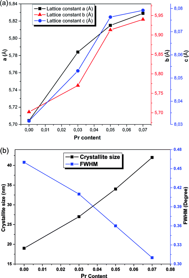 | ||
| Fig. 3 Calculated parameters of the pure and Pr-doped SrSnO3. (a) Lattice constants and (b) crystallite size and FWHM variation as a function of Pr content. | ||
Vibrational analysis of the material under investigation is essential to emphasize the purity and crystallinity of the prepared samples and to identify the dopant insertion effect on the vibrational modes of the pristine structure. Therefore, this part consisted of an in-depth analysis of the samples employing both FT-IR and typical Raman analysis at room temperature. The FT-IR analysis results of the films with different concentrations of Pr recorded at room temperature within the region of 450–2000 cm−1 are shown in Fig. 4. The orthorhombic phase of SrSnO3 with the Pbnm space group had 25 IR active modes at Γ of the Brillouin zone, given by the irreducible representations:
| ΓIR = 9B1u + 7B2u + 9B3u | (3) |
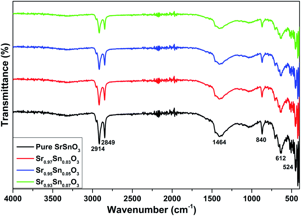 | ||
| Fig. 4 FT-IR spectra of the Sr1−xPrxSnO3 (x = 0, 3, 5 and 7 at%) thin films. | ||
The undoped sample showed multiple modes at different positions, starting with the widest one at 1464 cm−1, which was attributed to the N–O band linked to the nitrate present in the precursors. The bands between 2800 and 3000 cm−1 were assigned to different types of O–H stretching. The band at 1033 cm−1 was attributed to the asymmetric stretching vibration of Sn–OH bonds, while the bands located at 840 cm−1 were attached to O–Sn–O asymmetric stretching vibration of SnO3. The band at 612 cm−1 was due to the presence of stannate (SnO32−) vibrations.26 The peak located at 524 cm−1 was attached to the presence of stretching vibrations of Sn–O bands, and this trend confirmed the existence of SnO6 octahedral tilting in all the compounds.27,28 Several extra weak peaks appeared between 400 and 500 cm−1 and were associated with the Pr–O molecular vibrations originating from the octahedral coordination PrO6. Indeed, the FT-IR analysis results confirmed the presence of metal–oxygen vibrations with the detection of other active IR modes, which was consistent with the XRD analysis and confirmed the effective formation of the SrSnO3 compound in the orthorhombic structure.
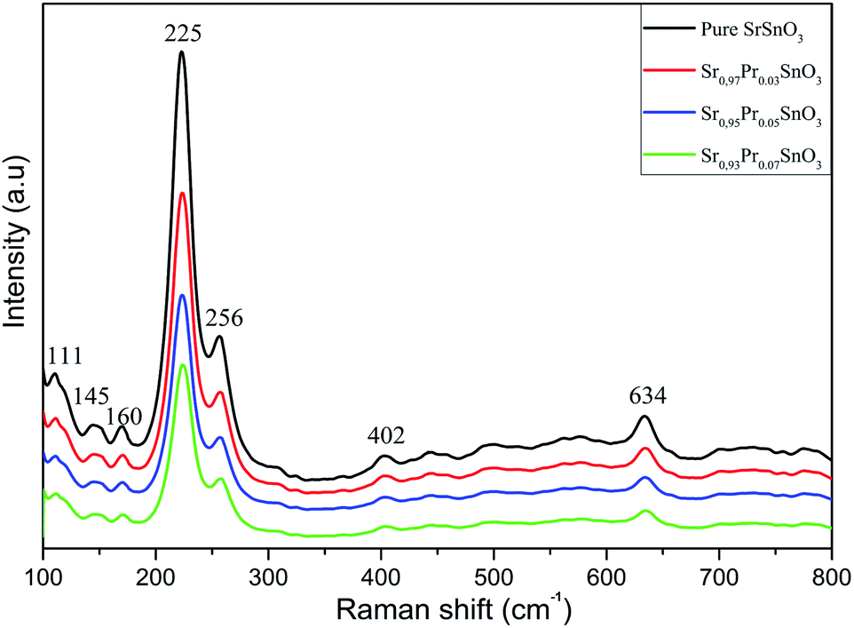
Raman analysis of the samples collected at room temperature was performed to determine the local structure of the samples, to better inspect the presence of secondary phases, and to identify the Pr doping effect on the vibrational modes of the pristine structure, as presented in Fig. 5. According to previous extensive Raman analysis, the orthorhombic phase of SrSnO3 has 24 active Raman modes presented as follow:
| ΓRaman = 7Ag + 5B1g + 7B2g + 5B3g | (4) |
 | ||
| Fig. 5 Raman spectra of the pure and Pr-doped SrSnO3 thin films collected at room temperature. | ||
The equation contains four antisymmetric with two symmetric octahedral stretching modes, four bending modes, and six octahedral rotation or tilt modes. The remaining eight modes are associated with the strontium cations. The Raman analysis of the undoped SrSnO3 thin film revealed several vibrational modes with two intense peaks located at 225 and 256 cm−1, corresponding both to the Ag mode.26 Multiple other peaks were detected at 111, 145, 160, 402 and 634 cm−1 and also matched with the usually recorded Raman modes for orthorhombic (Pbnm) SrSnO3.26,29 All these modes were due to the first-order Raman scatterings, which is a signature of distortion from the ideal cubic perovskite because, in ideal perovskites, no first-order Raman scattering is possible.13 As the dopant ratios were inserted, a slight shifting in position was observed, particularly for the main modes. The Ag active mode for the doped samples showed a slight shift towards a higher wavenumber (231 cm−1) when compared to the undoped film (225 cm−1). This revealed that the Pr3+ cations had effectively replaced the Sr2+ sites and consequently affected the Sr–O bonds. No change in modes was observed. Thus, the doping process had no effect on changing the modes or altering the structural properties of the pure sample. Furthermore, an intense decrement of the modes intensities was observed with a slight fading of the smaller modes. The Raman analysis, thus, further authenticated the formation of the orthorhombic SrSnO3 (Pbnm) compound with high crystallinity.
Morphological properties scanning is a substantial step in evaluating the quality of prepared samples and thereby their effect on the stacking and construction of the anticipated devices. Hence, a full thorough scanning of the surface quality was performed by means of field emission scanning electron microscopy (FE-SEM) alongside energy dispersive spectroscopy (EDX) to evaluate the modifications induced by Pr doping on the quality, grain size and composition of the films. Fig. 6 exhibits the FE-SEM images of the pure and Pr-doped SrSnO3 films deposited onto Si (100) substrate and annealed at 800 °C. Fig. 6a displays a top-view image of the prepared film. The samples generally possessed textured, crack-free and homogeneous surfaces with a uniform distribution along the substrate. The image manifests the efficiency of the synthesis route followed in producing high-quality and uniform films. Moreover, the micrograph in Fig. 6b displays the formation of high-density nanorods with varying sizes for the pure film. It is noticeable from the images that small spherical grains were formed, which may be attributed to the limited number of Sr and Sn clusters and secondary phases. By increasing the dopant content, an augmentation of the size of the nanorods was observed and the size continued to increase as the dopant fraction increased, as presented in Fig. 6c. This augmentation demonstrated the effective insertion of Pr ions in SrSnO3 pristine lattice, as mentioned earlier in the structural analysis results, indicating the correlation between the structural and morphological results. Fig. 6d displays a cross-sectional view of the prepared films. The thicknesses of the films were measured as being between 180 and 200 nm, indicating the high quality of the prepared samples and their compatibility for facile device stacking.
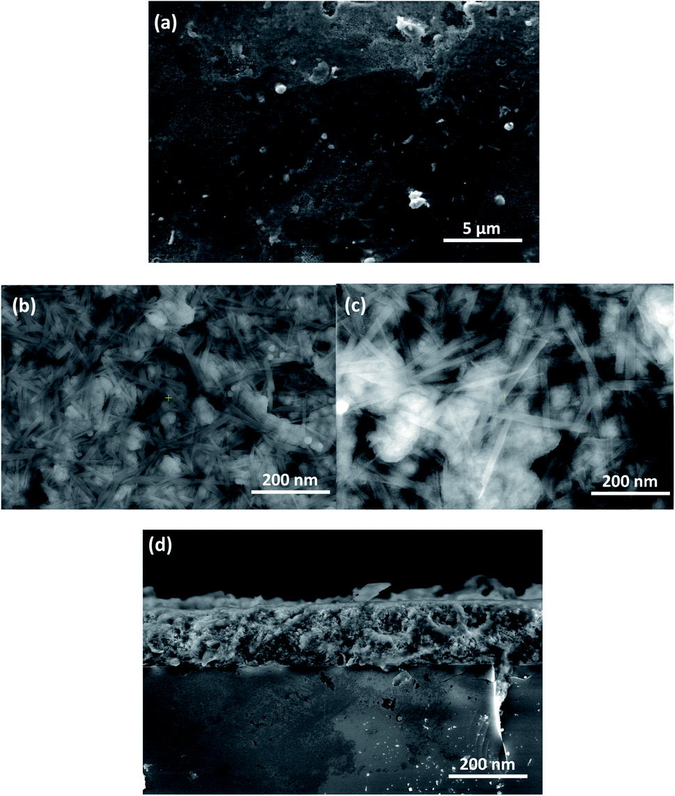 | ||
| Fig. 6 FE-SEM scanning images for the pure and Pr-doped SrSnO3 nanorod thin films. Top view of the films (a) and close view (b) of the pure and (c) 7% (Pr content) doped films. (d) Cross-sectional view of the deposited films. | ||
EDX analysis and atomic mapping were performed to analyze the compositional elements of the prepared samples and the distribution of the elements along the prepared surfaces. Fig. 7a illustrates the EDX data collected for the pure and doped samples. The results confirmed the presence of sufficient quantities of the main elements (Sr, Sn, O), indicating the high purity and near-stoichiometric nature of the samples with a rich oxygen content. The detected Si signal was assigned to the Si (100) substrate as a result of the difference between the thicknesses of the films and the high EDX interaction volume and penetration depth of the electron beam. This may slightly reduce the accuracy of the EDX quantitative analysis. Furthermore, the existence of the dopant element Pr was confirmed in the doped films with the variant ratios added as gathered in Table 1. The stoichiometry was slightly unbalanced as the dopant ratios increased. Furthermore, elemental atomic mapping was implemented to further probe the distribution of the elements along the surfaces and their quantification with high precision. The mapping images confirmed the presence of the main elements with equal distribution along the surfaces of films. In addition, the images show an orderly repartition of the elements with a higher concentration for the oxygen element and a small fraction for the Pr element.
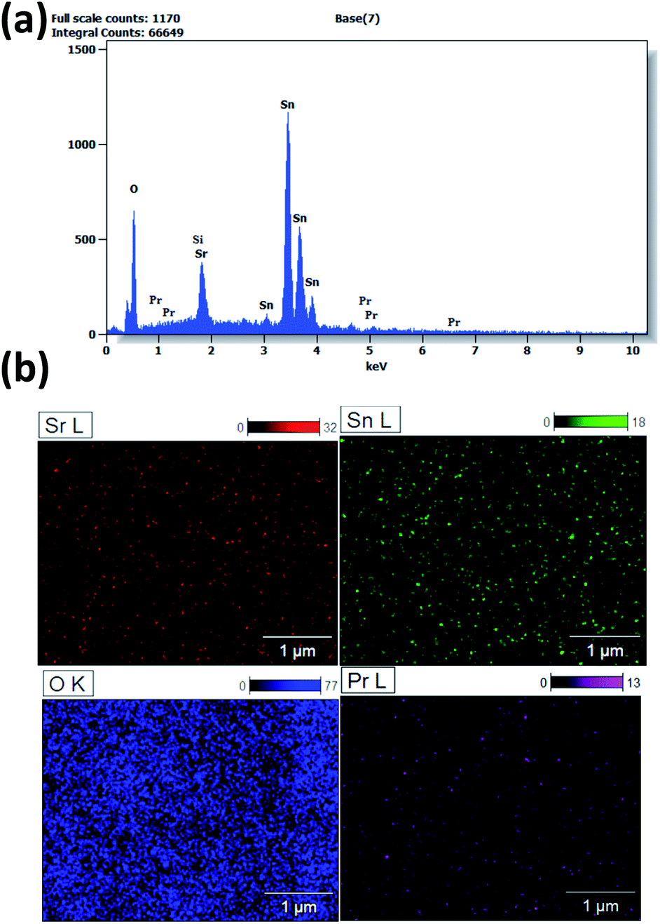 | ||
| Fig. 7 (a) EDX analysis spectrum and (b) atomic mapping (Sr, Sn, O, Pr) images of Pr-doped SrSnO3 thin films. | ||
| Samples | Atomic percentages | |||
|---|---|---|---|---|
| Sr | Sn | O | Pr | |
| SrSnO3 | 23.93 | 24.21 | 51.86 | 0 |
| SrSnO3:Pr3+ (3%) | 23.73 | 24.19 | 51.28 | 0.8 |
| SrSnO3:Pr3+ (5%) | 23.49 | 24.24 | 51.07 | 1.2 |
| SrSnO3:Pr3+ (7%) | 23.37 | 24.22 | 50.71 | 1.7 |
Since rare-earth elements are well known as an effective dopant commonly used to engineer the optical properties of metal oxides, the optical properties of the films were collected to assess the trivalent Pr3+ insertion effect on the absorption and band gap tuning of the pristine film. Consequently, the UV-Vis-NIR absorption spectra of the pure and Pr-doped SrSnO3 thin films are illustrated in Fig. 8a. All the films exhibited strong absorption in the UV light region (200–400 nm), with a notable decrement in the visible region, which continued to decrease exponentially as the wavelength value increased in the near-infrared (NIR) region. The absorption edge of the doped films was slightly shifted towards higher wavelengths as the Pr fractions increased. In addition, the dopant incorporation caused the absorption to decrease in the UV light region and increase in the visible region and onward, showing a reverse trend from the undoped film. The results manifested the effect of Pr3+ insertion on tuning the optical properties of metal oxide materials, which has been reported before.17 It could be clearly seen that the doping process enhanced the photon-absorption ability of the films in the visible and near-infrared region, which is quite suitable for optoelectronic applications. To further evaluate the doping effect on the band gap of the samples, the band gaps of the pristine and Pr-doped SrSnO3 were calculated using a Tauc plot:
| (αhν) = A(hν − Eg)n | (5) |
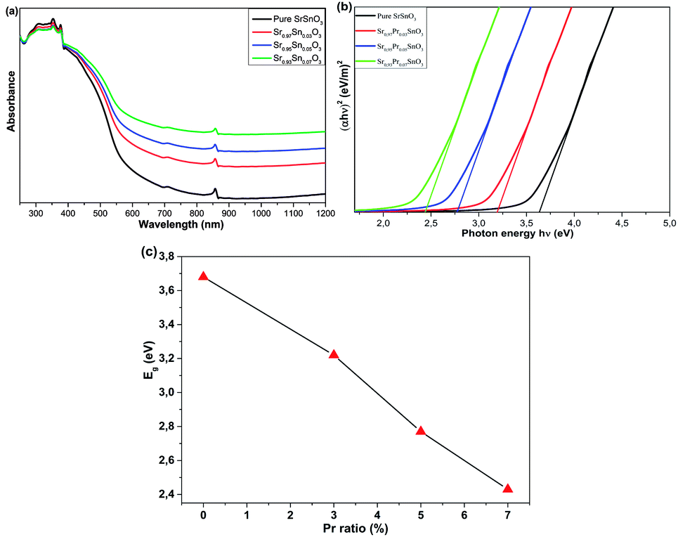 | ||
| Fig. 8 (a) Optical absorbance as a function of the wavelength. (b) The plots of (αhν)1/2 versus hν and (c) band gap variation of the pristine and Pr-doped SrSnO3 thin films. | ||
This part consists of theoretical calculations that were mainly carried out to uncover the nature of the bonds formed between the different elements and to investigate the electronic and optical properties of the material under investigation. Herein, the calculations were conducted in order to strengthen the experimental findings regarding the properties of the pristine material and to inspect the effect of the strongly correlated 4f state of Pr insertion on the electronic and optical properties of the SrSnO3 perovskite compound. Therefore, the results from first-principle calculations will permit an overall assessment of the alterations on the properties of the material under investigation. Fig. 9 exhibits the projectile and total density of states of the pure and Pr-doped SrSnO3 compounds calculated using LDA and SIC-LDA approximations as a function of energy. For the dos produced by regular LDA, the conduction band minima (CB) of SrSnO3 is composed essentially of Sr-3d states and a negligible contribution from O-2p, while the valence band maxima (VB) is largely dominated by the O-2p states. The calculated band gap was estimated at 2.46 eV. Commonly, regular LDA approximation usually tends to underestimate the optical and electronic properties of the material under investigation, leading to the non-consideration of the exchange and the correlation effects in metal oxide materials and causing important self-interaction errors.30 This underestimation of the band gap by LDA is due to the lack of a discontinuity in this exchange–correlation potential. Thus, the self-interaction correction (SIC) was integrated to enhance the accuracy of the obtained properties. LDA-SIC approximation is generally viewed as an extension of regular LDA, where the Kohn–Sham wave function is projected onto a set of localized basis orbital's and the SIC approximation is governed by the energy difference between the energy gain due to hybridization of the orbital with the valence band and the energy gain upon localization of the orbital.31 After the SIC correction, the band gap increased to reach 3.12 eV as expected. Typically, doping a semiconductor obligates the Fermi level to shift towards higher energy values due to the fact that the doping process enhances the stability of the compound corresponding to the low energies. Plus, the Fermi energy shifts towards the conduction band after doping and this is due to the fact that the valence band shifts into the lower energy region much more than that of the conduction band. The application of SIC approximations permitted properly dealing with the 4f states in SrSnO3 lattice doped with the rare-earth (RE = Pr) compound due to the existence of f-electrons. As for the SIC-LDA approximation, the same applies to the conduction band, with growing domination from the O-2p states spotted in the valence band, as can be seen from Fig. 9. After the first doping percentage was inserted, a major contribution from the Pr-4f states was observed, especially in the valence band, and the band gap decreased to 2.53 eV. For the 7% Pr content, we can notice that the contribution of the Pr-4f states increased and dominated both the valence and conduction bands, leading the band gap to shrink and further reduce to 2.12 eV. This decrease in the band gap was mainly attributed to the 3d–4f strong exchange interactions. Previous works reporting rare-earth doping indicated a similar outcome; for instance, Abdul Majid et al. reported that the 3d–4f exchange interactions are more fragile than 3d–3d because of the strongly localized nature of 4f orbitals in rare-earth atoms.32 A first proposition that provided an explanation of 3d–4f interactions was suggested by Campbell.33 Similar to that, Brooks et al. further discussed in detail how 4f localized electrons polarize 5d states, which then interact with 3d orbitals.34 Indeed, the DFT calculations permitted an accurate and overall analysis of the electronic and optical properties of the pristine compound alongside inspecting the effect of the rare-earth (praseodymium) doping on engineering its properties in a constructive manner. The results confirmed the fact that the Pr3+ incorporation enhanced the optical and electrical properties of the samples.
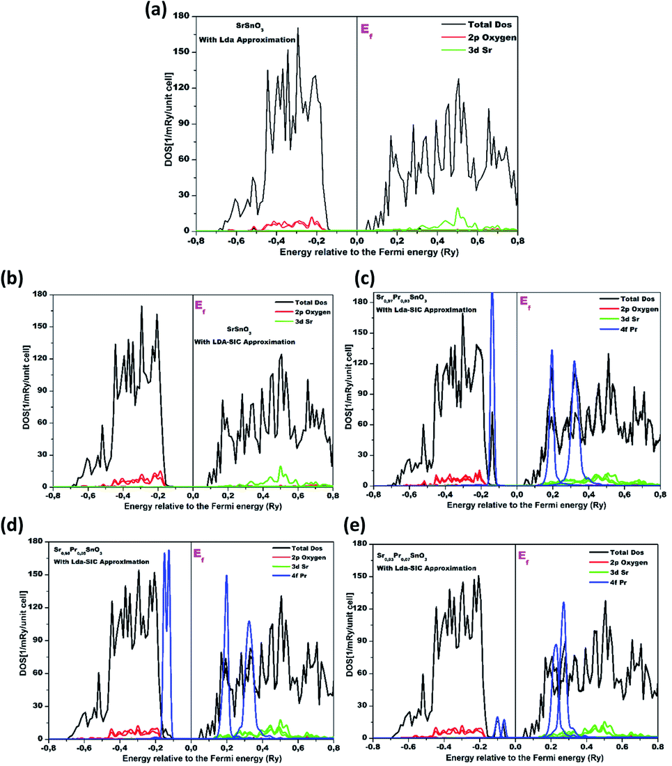 | ||
| Fig. 9 Calculated partial and total density of states of the pure and Pr-doped SrSnO3 (a) 0% with LDA approximation, and (b) 0% with LDA-SIC, (c) 3%, (d) 5% and (e) 7% Pr content. | ||
Assessing the electrical properties of thin film materials and the defects generated from impurities insertion is essential to evaluate their potential for optoelectronic applications. Therefore, it is important to conduct a thorough evaluation of the electrical properties of the prepared samples and the alterations resulting from the doping process, thereby evaluating their potential for further applications. The electrical properties of the pure and Pr-doped SrSnO3 thin films were collected at T = 300 K to unveil the semiconducting nature of the films, and to examine the alterations on the conductivity and carrier mobility generated from the Pr3+ doping effect. Fig. 10 displays the collected electrical properties employing the van der Pauw configuration in the presence of a magnetic field and their variation as a function of doping content. The values of the Hall coefficient (RH) indicated that all the samples had n-type conductivity, as indicated previously.16,17 As for the films resistivity, an immense decrement was observed upon the doping ratios increase passing from 7.3 × 10⁻² Ω cm for the undoped sample to 4.8 × 10⁻² Ω cm for 7% Pr content. This proves once again that rare-earth element doping (in our case praseodymium) is effective in enhancing the conductivity of oxide thin film materials. For the carrier concentration, a reverse tendency to the resistivity was detected, where the value for the undoped sample jumped from 3.4 × 10¹⁹ to 6.1 × 1019 cm−3 for 7% Pr content. The same variation was noticed on the carrier mobility, which increased from 2.5 to 7.6 cm2 V−1 s−1. The increment of the carrier mobility by the doping insertion effect was suggested earlier by the structural results and FE-SEM scanning by the augmentation in the nanorod sizes. Thus, the Pr-doped SrSnO3 thin film possessed superior electrical properties in comparison to the pristine material, showing the capability of Pr3+ as a dopant to enhance the characteristics of stannous-based perovskite oxides.
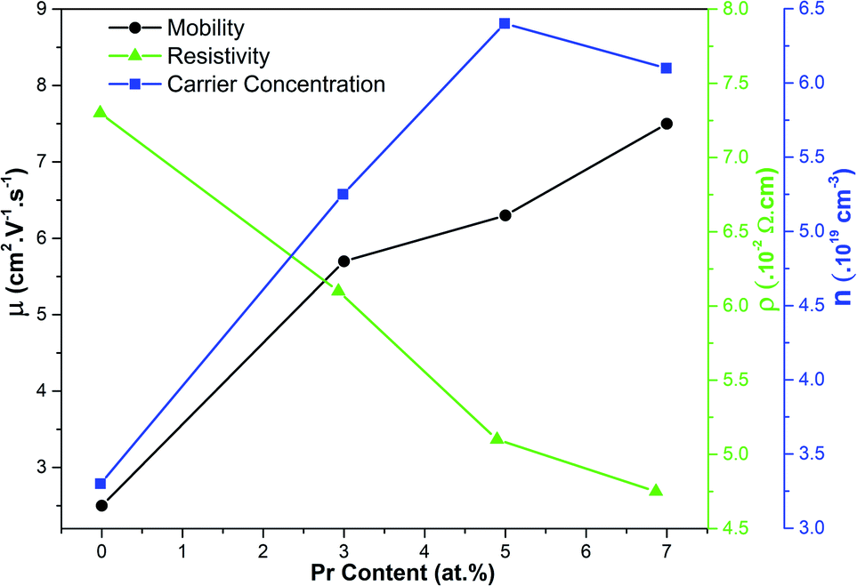 | ||
| Fig. 10 Electrical properties (resistivity, carrier concentration, and mobility) of the pure and Pr-doped SrSnO3 films as a function of Pr content collected at room temperature. | ||
5. Conclusions
In summary, a facile, two-step route was developed to synthesize high-quality Pr-doped SrSnO3 onto a Si (100) substrate as highly conductive and transparent oxide thin films via a simple chemical solution method. Microstructural analysis revealed that the increase in Pr substitution at the Sr sites enhanced the phase quality and fostered its stability. Plus, the type of substrate used had no effect on the quality of the phase. Morphological scanning revealed the nanorod nature of the samples and the constructive effect of the Pr doping ratios on the quality of the films. An increment in the films optical absorption was noticed as the doping content increased together with wide band gap tuning. First-principle calculations allowed the identification of extremely correlated 4f-related electronic states (with the Pr) effect on the SrSnO3 electronic and optical properties. Hall-effect measurements showed an increment in the carrier mobility and a decrease in the resistivity with superior characteristics as the doping fractions increased. Overall, the facile synthesis route, tunable properties, enhanced optical absorption and electrical properties of the nanorod morphology Pr-doped SrSnO3 thin films are encouraging for future integration in optoelectronic applications.Conflicts of interest
There are no conflicts to declare.Notes and references
- Y. Chen, Q. Meng, L. Zhang, C. Han, H. Gao, Y. Zhang and H. Yan, SnO2-based electron transporting layer materials for perovskite solar cells: A review of recent progress”, J. Energy Chem., 2019, 35, 144–167 CrossRef.
- P. Prathap, A. S. Dahiya, M. Srivastava, S. K. Srivastava, B. Sivaiah, D. Haranath, P. Vandana, R. Srivastava, C. M. S. Rauthan and P. K. Singh, “Anti-reflection In2O3 nanocones for silicon solar cells”, Sol. Energy, 2014, 106, 102–108 CrossRef CAS.
- D.-K. Hwang, M.-S. Oh, J.-H. Lim and S.-J. Park, “ZnO thin films and light-emitting diodes”, J. Phys. D: Appl. Phys., 2007, 40, R387–R412 CrossRef CAS.
- J. F. Scott, R. Palai, A. Kumar, M. K. Singh, N. M. Murari, N. K. Karan and R. S. Katiyar, New Phase Transitions in Perovskite Oxides: BiFeO3, SrSnO3, and Pb(Fe2/3W1/3)1/2Ti1/2O3, J. Am. Ceram. Soc., 2008, 91, 1762–1768 CrossRef CAS.
- C. P. Udawatte, M. Kakihana and M. Yoshimura, Preparation of Pure Perovskite-Type BaSnO3 Powders by the Polymerized Complex Method at Reduced Temperature, Solid State Ionics, 1998, 108, 23–30 CrossRef CAS.
- J. James, O. B. S. Kumar, S. S. Kumar, P. P. Rao and K. V. O. Nair, Nanoparticles of Ba2MSnO6−x (M = Ce, La and Nd; x = 0 or 0.5): a new group of complex perovskite oxides, Mater. Lett., 2003, 57, 3641–3647 CrossRef CAS.
- F. Zhong, H. Zhuang, Q. Gu and J. Long, Structural evolution of alkaline earth metal stannates MSnO3 (M = Ca, Sr, and Ba) photocatalysts for hydrogen production, RSC Adv., 2016, 6, 42474–42481 RSC.
- H. Guo, H. Chen, H. Zhang, X. Huang, J. Yang, B. Wang, Y. Li, L. Wang, X. Niu and Z. Wang, Low-temperature processed yttrium doped SrSnO3 perovskite electron transport layer for planar heterojunction perovskite solar cells with high efficiency, Nano Energy, 2019, 59, 1–9 CrossRef CAS.
- H. Guo, H. Zhang, J. Yang, W. Gong, H. Chen, H. Wang, X. Liu, H. Feng, X. Niu and Y. Zhao, Lanthanum-Doped Strontium Stannate for Efficient Electron- Transport Layers in Planar Perovskite Solar Cells, ACS Appl. Energy Mater., 2020, 3(7), 6889–6896 CrossRef CAS.
- C. W. Myung, G. Lee and K. S. Kim, La-doped BaSnO3 electron transport layer for perovskite solar cells, J. Mater. Chem. A, 2018, 6, 23071–23077 RSC.
- S. S. Shin, E. J. Yeom, W. S. Yang, S. Hur, M. G. Kim, J. Im, J. Seo, J. H. Noh and S. Il Seok, Colloidally prepared La-doped BaSnO3 electrodes for efficient, photostable perovskite solar cells, Science, 2017, 356, 167–171 CrossRef CAS PubMed.
- Y. Kumar, R. Kumar, R. J. Choudhary, A. Thakur and A. P. Singh, Reduction in the tilting of oxygen octahedron and its effect on bandgap with La doping in SrSnO3, Ceram. Int., 2020, 46, 17569–17576 CrossRef CAS.
- J. M. Li, C. H. A. Huan, Y. W. Du, D. Feng and Z. X. Shen, Magnetic-field-tunable charge carrier localization in sintered polycrystalline La0.75Ca0.25MnO3, Phys. Rev. B: Condens. Matter Mater. Phys., 2001, 63, 1–5 Search PubMed.
- L. Chantelle, A. L. Menezes de Oliveira, B. J. Kennedy, J. Maul, R. Márcia, S. da Silva, T. M. Duarte, A. R. Albuquerque, J. R. Sambrano, R. Landers, M. Siu-Li, E. Longo, M. Iêda and G. dos Santos, Probing the Site-Selective Doping in SrSnO3: Eu Oxides and Its Impact on the Crystal and Electronic Structures Using Synchrotron Radiation and DFT Simulations, Inorg. Chem., 2020, 59(11), 7666–7680 CrossRef CAS PubMed.
- H. Shaili, E. M. Salmani, M. Beraich, R. Essajai, W. Battal, M. Ouafi, A. Elhat, M. Rouchdi, M. Taibi, H. Ez-Zahraouy, N. Hassanain and A. Mzerd, Enhanced properties of the chemically prepared Gd-doped SrSnO3 thin films: Experimental and DFT study, Opt. Mater., 2020, 107, 110136 CrossRef CAS.
- K. Li, Q. Gao, L. Zhao and Q. Liu, Transparent and conductive Sm-doped SrSnO3 epitaxial films, Opt. Mater., 2020, 107, 110139 CrossRef CAS.
- Q. Liu, J. Dai, X. Zhang, G. Zhu, Z. Liu and G. Ding, Perovskite-type transparent and conductive oxide films: Sb- and Nd-doped SrSnO3, Thin Solid Films, 2011, 519, 6059–6063 CrossRef CAS.
- H. Wakana, K. Ai, S. Adachi, K. Nakayama, Y. Ishimaru, Y. Tarutani and K. Tanabe, Examination of deposition conditions for SrSnO3 insulating layer for single flux quantum circuits, Phys. C, 2005, 426–431(2), 1495–1501 CrossRef CAS.
- M. C. F. Alves, R. M. M. Marinho, G. P. Casali, M. Siu-Li, S. Deputier, M. Guilloux-Viry, A. G. Souza, E. Longo, I. T. Weber, I. M. G. Santos and V. Bouquet, Influence of the network modifier on the characteristics of MSnO3 (M = Sr and Ca) thin films synthesized by chemical solution deposition, J. Solid State Chem., 2013, 199, 34–41 CrossRef CAS.
- M. Beraich, H. Shaili, E. Benhsina, Z. Hafidi, M. Taibi, F. Bentisse, A. Guenbour, A. Bellaouchou, A. Mzerd, A. Zarrouk and M. Fahoume, Experimental and theoretical study of new kesterite Cu2NiGeS4 thin film synthesized via spray ultrasonic technic, Appl. Surf. Sci., 2020, 527, 146800 CrossRef CAS.
- H. Shaili, M. Beraich, A. El hat, M. Ouafi, E. M. Salmani, R. Essajai, W. Battal, M. Rouchdi, M. Taibi, N. Hassanain and A. Mzerd, Synthesis of the Sn-based CaSnS3 chalcogenide perovskite thin film as a highly stable photoabsorber for optoelectronic applications, J. Alloys Compd., 2021, 851, 156790 CrossRef CAS.
- H. Shaili, E. Salmani, M. Beraich, A. Elhat, M. Rouchdi, M. Taibi, H. Ez-Zahraouy, N. Hassanain and A. Mzerd, Revealing the impact of strontium doping on the optical, electronic and electrical properties of nanostructured 2H-CuFeO2 delafossite thin films, RSC Adv., 2021, 11, 25686–25694 RSC.
- H. Akai, http://sham.phys.sci.osaka-u.ac.jp/%7Ekkr/.
- M. Toyoda, H. Akai, K. Sato and H. Katayama-Yoshida, Electronic structures of (Zn, TM) O (TM: V, Cr, Mn, Fe, Co, and Ni) in the self-interaction- corrected calculations, Phys. B, 2006, 376–377, 647–650 CrossRef CAS.
- E. Baba, D. Kan, Y. Yamada, M. Haruta, H. Kurata, Y. Kanemitsu and Y. Shimakawa, Optical and transport properties of transparent conducting La-doped SrSnO3 thin films, J. Phys. D: Appl. Phys., 2015, 48, 455106 CrossRef.
- M. C. F. Alves, M. R. Nascimento, J. Severino, G. Lima, P. S. Pizani, J. W. M. Espinosa, E. Longo, E. Luiz, B. Soledade, A. G. Souza and I. M. G. Santos, Influence of synthesis conditions on carbonate entrapment in perovskite SrSnO3, Mater. Lett., 2009, 63, 118–120 CrossRef CAS.
- N. Jain, D. K. Pandey, R. K. Singh, J. Singh and R. A. Singh, Study of Ce3+, Dy3+ and Eu3+ Activated SrSnO3 for White LEDs, AIP Conf. Proc., 2018, 1953, 030125 CrossRef.
- M. Muralidharan, R. Thiyagarajan, K. Sivakumar and K. Sivaji, Near infrared emission and enhanced ferromagnetism in Fe doped SrSnO3 perovskite structured nanorods, J. Mater. Sci.: Mater. Electron., 2019, 30, 4634–4643 CrossRef CAS.
- E. Moreira, J. M. Henriques, D. L. Azevedo, E. W. S. Caetano, V. N. Freire and E. L. Albuquerque, Structural, optoelectronic, infrared and Raman spectra of orthorhombic SrSnO3 from DFT calculations, J. Solid State Chem., 2011, 184, 921–928 CrossRef CAS.
- F. Z. Chafi, E. Salmani, L. Bahmad, N. Hassanain, F. Boubker and A. Mzerd, First principle calculations with SIC correction of Fe-doped CuO compound”, Comput. Condens. Matter, 2018, 16, e00304 CrossRef.
- J. P. Perdew and A. Zunger, Self-interaction correction to density functional approximations for many-electron systems, Phys. Rev. B: Condens. Matter Mater. Phys., 1981, 23, 5048–5079 CrossRef CAS.
- A. M. A. Dar, A density functional theory study of 3d–4f exchange interactions in Cr–Nd codoped GaN, J. Magn. Magn. Mater., 2014, 368, 384–392 CrossRef.
- I. A. Campbell, Indirect exchange for rare earths in metals, J. Phys. F: Met. Phys., 1972, 2, L47 CrossRef CAS.
- B. Q. Ma, S. Gao, G. Su and G. X. Xu, Cyano-Bridged 4f–3d Coordination Polymers with a Unique Two-Dimensional Topological Architecture and Unusual Magnetic Behavior, Chem. Int. Ed., 2001, 40, 434–437 CrossRef CAS.
| This journal is © The Royal Society of Chemistry 2021 |