DOI:
10.1039/D1RA06828H
(Paper)
RSC Adv., 2021,
11, 37218-37224
Surface plasmon coupling regulated CsPbBr3 perovskite lasers in a metal–insulator–semiconductor structure†
Received
11th September 2021
, Accepted 8th November 2021
First published on 19th November 2021
Abstract
A strong coupling effect often occurs between a metal and semiconductor, so micro/nano-lasers based on surface plasmons can break through the optical diffraction limit and realize unprecedented linear and nonlinear enhancement of optical processes. Hence, metal–insulator–semiconductor (M–I–S) structures based on perovskite materials were explored to design optoelectronic devices. Herein, we constructed an Ag/SiO2/CsPbBr3 hybrid structure to generate surface plasmon coupled emission between the metal and CsPbBr3 perovskite. Combined with experimental characterization and COMSOL Multiphysics software simulations, the best enhancement for CsPbBr3 radiative recombination efficiencies can be achieved with a 10 nm-thickness of the SiO2 layer and 80 nm-thickness of the Ag metal film, further verified by optimizing the thickness of the SiO2 layer above the Ag metal film. In this state, the laser threshold can be as low as 0.138 μW with a quality (Q) factor of up to 3907 under optical pumping, which demonstrate a significant step toward practical applications in biological technology, chemical identification, and optical interconnections of information transmission.
Introduction
Nowadays, the emerging trihalide perovskite materials are considered as promising candidates to achieve high quality micro/nanoscale lasing devices and have attracted tremendous attention from researchers, mainly benefitting from their outstanding characteristics, such as high photoluminescence (PL) quantum yields (∼100%), narrow emission bandwidths, long charge-diffusion length, high absorption coefficient, low-cost fabrication routes, and so on.1–9 Owing to these salient features, the development of high-quality perovskite lasers with tunable emission wavelength has accelerated quickly through intensive research efforts in the past decades,10–13 and they were realized successfully using Fabry–Pérot (F–P) and whispering gallery mode (WGM) resonators based on single crystals of micro-nanostructured perovskites and applied in various fields, such as high-density data storage, large-scale optoelectronic integration, and high-resolution optical imaging.14–17 Afterwards, with the development of materials and technology, the laser research hotspot turns gradually to focus in the direction of smaller volume, higher power, higher efficiency, and faster modulation speed. And more and more attention was devoted to the coupling paths through metal–insulator layers with perovskite materials to generate surface plasmon resonance, which could break optical diffraction limit and enhance plasmon coupling efficiency compared to conventional semiconductor lasers, even though when their physical dimension and optical mode volume were scaled down to the subwavelength range.18–20 In 2003, the concept of surface plasmon amplification by stimulated emission of radiation (SPASER) was proposed by M. I. Stockman and D. J. Bergman, as a promising method for shrinking the lasing device to the nanoscale.21–23 Subsequently, various plasmons with perovskite resonant cavities were triggered explosive development and investigated drastically.24–28 For example, Cheng et al. conducted in full-spectrum modeling that featured hybrid perovskite nanowires placed on different SiO2-coated metallic (Au, Ag, and Al) plates, the corresponding experimental results for the MAPbBr3 nanolaser on Ag revealed the low-threshold operation at approximately 1.62 μW average power.29 In addition, Yu et al. demonstrated plasmonic laser action using a hybrid geometry whereby the MAPbI3 perovskite nanowires were placed on an Ag substrate with an insulating spacer layer. Relatively low threshold operation under ambient condition (13.5 μJ cm−2) was reported, and the device could work well even at temperatures up to 43.6 °C. However, as is known to all, using organic–inorganic hybrid perovskites as high gain medium still exists several issues, mainly due to their physical and chemical stability are poor compared to all-inorganic perovskite materials when exposed to environments under heat and humidity conditions.30,31 At the moment, the newly developed all-inorganic perovskite materials (CsPbX3, X = Cl, Br, I) exhibit unprecedented light harvesting and light-emitting properties in the field of small laser devices. In especial, CsPbBr3 perovskite materials stand out and display remarkable characteristics, owing to their highly improved optical performance and thermal stability, high quantum yield, and low trap state density, which enable them to be the promising alternative materials for realizing low-threshold plasmonic lasers, where high optical gain is essential. In 2016, Eaton et al. first reported the application of all-inorganic perovskite nanowires in the laser field.32 They prepared CsPbBr3 and CsPbCl3 nanowires successfully by the liquid-phase cryogenic solution method and used them as gain media. Under pulsed laser excitation, the lasing threshold of CsPbBr3 nanowires was 5 μJ cm−2, and the maximum quality factor was about 1009. Meanwhile, the experimental results provided evidence for the correctness of the electron–hole plasma mechanism. Compared with the previously reported organic–inorganic hybrid perovskite, all-inorganic perovskite exhibited better stability. Lasing under constant, pulsed excitation can be maintained for over 1 h, the equivalent of 109 excitation cycle.33
Experimental section
In this work, the CsPbBr3 perovskite samples were obtained by using the anti-solvent crystallization technique. 0.2 M of CsBr and a PbBr2 solution were mixed together with a volume ratio of 1![[thin space (1/6-em)]](https://www.rsc.org/images/entities/char_2009.gif) :1 in anhydrous N,N-dimethylformamide (DMF) and then gently shaken until their complete dissolution, and formed CsPbBr3 crystals with desirable diffusion eventually. Afterwards, the CsPbBr3 solution was dispersed onto a silicon and M–I–S structures, respectively, and sealed in a beaker to control the evaporation rate. After about 24 hours at room temperature, CsPbBr3 micro-cubes were prepared on the substrates. It's noted that the insulator SiO2 thickness in M–I–S structures was designed as 10 nm, 30 nm, and 60 nm between the CsPbBr3 semiconductor and Ag metal layer, and they were marked as sample B, C, and D, severally, while the prepared sample in bare silicon substrate was marked as sample A. Remarkably, M–I–S structures were fabricated successfully using the following steps: Firstly, 200 nm-thickness of SiO2 layer was grown on the Si substrate by plasma enhanced chemical vapor deposition (PECVD). Secondly, 80 nm-thickness of Ag film was placed on the above SiO2 layer by electron beam evaporation. And finally, different thickness of SiO2 layer was grown on Ag film by PECVD to act as the insulator layer. The detailed descriptions were listed in Table 1.
:1 in anhydrous N,N-dimethylformamide (DMF) and then gently shaken until their complete dissolution, and formed CsPbBr3 crystals with desirable diffusion eventually. Afterwards, the CsPbBr3 solution was dispersed onto a silicon and M–I–S structures, respectively, and sealed in a beaker to control the evaporation rate. After about 24 hours at room temperature, CsPbBr3 micro-cubes were prepared on the substrates. It's noted that the insulator SiO2 thickness in M–I–S structures was designed as 10 nm, 30 nm, and 60 nm between the CsPbBr3 semiconductor and Ag metal layer, and they were marked as sample B, C, and D, severally, while the prepared sample in bare silicon substrate was marked as sample A. Remarkably, M–I–S structures were fabricated successfully using the following steps: Firstly, 200 nm-thickness of SiO2 layer was grown on the Si substrate by plasma enhanced chemical vapor deposition (PECVD). Secondly, 80 nm-thickness of Ag film was placed on the above SiO2 layer by electron beam evaporation. And finally, different thickness of SiO2 layer was grown on Ag film by PECVD to act as the insulator layer. The detailed descriptions were listed in Table 1.
Table 1 The detailed descriptions of four samples
| Sample |
Substrate |
SiO2 thickness |
Ag thickness |
SiO2 thickness |
| A |
Si |
|
|
|
| B |
Si |
200 nm |
80 nm |
10 nm |
| C |
30 nm |
| D |
60 nm |
The sample's crystal quality was characterized by using an X-ray powder diffractometer (XRD), and scanning electron microscopy (SEM) images and EDX spectra of sample microstructures were obtained by using a Zeiss Gemini 500 field emission scanning electron microscope operated at 5 kV. Focused ion beam (FIB) system was further employed to observe the cross-section area of sample. Meanwhile, a high-resolution transmission electron microscopy (HRTEM) test was carried out using FEI Tecnai G2 F20 S-TWIN device. For optical characterizations, samples were excited using a femtosecond laser at a wavelength of 325 nm (150 fs, 1 kHz) in a micro-photoluminescence system, and the PL spectra were collected by using a spectrometer (Spectra Pro-2500i, Acton Research Corporation). Time-resolved PL (TRPL) measurements were carried out by utilizing a streak camera (Optronis Optoscope sc-10). All measurements were executed at room temperature.
Results and discussion
Fig. 1(a) demonstrates the crystal structure diagram of CsPbBr3 perovskite sample, it owns the octahedral geometry. The positive monovalent Cs ion (azury ball) locates within the center of eight lead bromide octahedrons.34 As shown in Fig. 1(b), CsPbBr3 micro-cube is placed on an Ag/SiO2/CsPbBr3 hybrid structure. When it is pumped by a high power 325 nm femtosecond pulsed laser, here will emit strong green light. As the output power increases steadily, PL intensity increases abruptly at certain value and laser emission phenomenon can appear.
 |
| | Fig. 1 (a) Crystal structure diagram of CsPbBr3 perovskite material; (b) schematic of a CsPbBr3 micro-cube on a surface plasmon substrate pumped by a 325 nm femtosecond pulsed laser. | |
Fig. 2(a)–(d) show SEM images of four CsPbBr3 samples, respectively. It is found that the CsPbBr3 micro-cubes own very smooth surfaces and exhibit different morphology features and sizes, such as regular cube and cuboid shapes, and dimensions range from a few microns to dozens of microns, further indicating that the various morphology and sizes of CsPbBr3 samples can be prepared successfully. The crystal pattern and quality of CsPbBr3 samples continue to be detected. The XRD characterization was conducted in Fig. 2(e). The sharp peaks measured from sample B are consistent with the standard card JCPDS No. 54-0751 of CsPbBr3 crystal. And EDS elemental mapping was displayed in Fig. 2(f); the atomic ratio of Br/Pb is estimated to be 3:1. The mapping of elements can confirm the presence of Cs, Pb, and Br elements and uniform distribution in the micro-cube. All of these XRD, SEM, and EDS results demonstrate the high crystalline quality of acquired CsPbBr3 samples.
 |
| | Fig. 2 (a–d) SEM images of the as-obtained four samples, respectively; (e) XRD pattern of sample B; (f) the EDS elemental mapping for sample B. | |
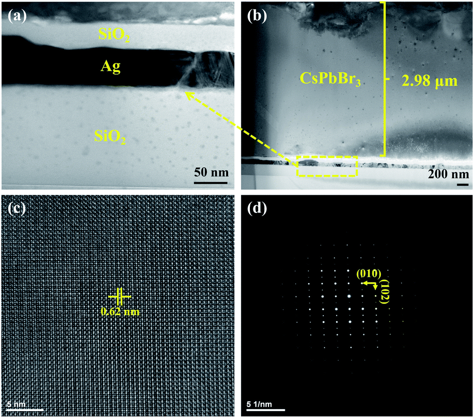
To further investigate the Ag/SiO2/CsPbBr3 hybrid structure, FIB-SEM test was carried out to character their cross-sections. The cross-sectional FESEM images of remaining samples B and C with varying layer thicknesses have been provided in Fig. S1.† Fig. 3(a) and (b) exhibit clear substrate and CsPbBr3 profiles of each layer interface. And the thickness of each layer can match well with our previous designed goal in Table 1. The thickness of CsPbBr3 perovskite layer above the M–I–S structure is about 2.98 μm. Furthermore, the corresponding HRTEM and SAED analyses were presented in Fig. 3(c) and (d), evidencing that the distinct lattice fringes are very regular and arrange orderly, the lattice distance is about 0.62 nm, which demonstrates the high crystalline quality of as-obtained sample D. More significantly, the crystal planes of (010) and (102) are consistent with XRD test in Fig. 2(e).
 |
| | Fig. 3 (a and b) Cross-sectional SEM images; (c) HRTEM image; and (d) selective-area electron diffraction (SAED) image of the as-obtained sample D, respectively. | |
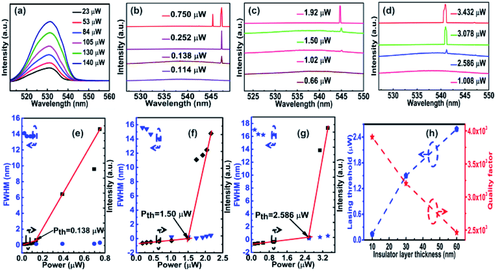
The lasing actions were investigated shown in Fig. 4. As displayed in Fig. 4(a), the PL intensity will increase quickly as the pump power increases from 23 μW to 140 μW. However, laser emission behavior is not observed, maybe due to the laser gain is not sufficient for sample A. By contrast, the typical single-mode lasing behaviors from CsPbBr3 micro-cubes can be achieved successfully, and the PL intensity increases abruptly when the output laser power increases to a certain value, which triggers off the laser emission behavior. Meanwhile, the ultra-low laser threshold is obtained and increases from 0.138 μW to 2.586 μW shown in Fig. 4(e)–(g), and the FWHM value can reach the minimum value of 0.14 nm for sample B with the laser emission wavelength at 547 nm. A high Q-factor of 3907 is calculated through the equation as follows shown in Fig. 4(h). As the insulator layer thickness increases, the lasing threshold increases, and Q decreases inversely. The optimized condition is 10 nm thickness of SiO2 layer above 80 nm thickness of Ag metal film just as mentioned before. Furthermore, the thinner below 10 nm or none SiO2 layer will make Ag metal film easier to oxidize, further resulting in generating material defects, increasing surface roughness, and improving the Ohm loss that affects the confinement of the electric field between CsPbBr3 perovskite and Ag metal film. This will supply an arena to boost the optoelectronic and laser applications of CsPbBr3 samples with high performance. Moreover, the acquisition of ultralow-threshold laser with CsPbBr3 perovskite is mainly ascribed to the well-designed M–I–S structure and high optical gain material, which can induce to generate strong exciton–photon coupling effect and increase the refractive index.18,35
where
λ and
δλ are the lasing mode wavelength and its FWHM, respectively.
 |
| | Fig. 4 Power dependent PL spectra of samples A (a), B (b), C (c), and D (d); (e–g) PL intensity and FWHM values from CsPbBr3 micro-cubes as a function of pump power; (h) lasing threshold and Q as a function of insulator layer thickness, respectively. | |
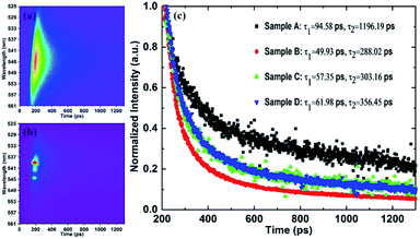
The streak camera images of sample B below (Fig. 5(a)) and above (Fig. 5(b)) the lasing threshold were used to study the carrier population dynamics for CsPbBr3-based laser cavity, and the emergence of a rapid decay component suggested fast carrier radiative recombination rate due to stimulated emission. In addition, as shown in Fig. 5(c), a standard two-exponential-component model was used to fit the decay traces.36,37
| | |
y = A1exp(−t/τ1) + A2exp(−t/τ2)
| (2) |
where
A1 and
A2 are constants,
τ1 and
τ2 are the fast and slow components of PL lifetime, respectively. Results exhibit that the carriers of CsPbBr
3 micro-cubes grown on M–I–S structures radiate faster than those in the bare Si substrate. Meanwhile, as the insulator layer SiO
2 thickness increases, the decay time
τ1 and
τ2 increase from 49.93 picosecond (ps) to 61.98 ps and from 288.02 ps to 356.45 ps, respectively. The fast decay rates illustrate that additional recombination channels for CsPbBr
3 micro-cubes are established
via using M–I–S structures, verifying that the effect of M–I–S structures is prominent. And the carrier recombination rate of sample B is faster than others, which proves that it owns the optimal performance among them currently.
 |
| | Fig. 5 Streak camera images of sample B below (a) and above (b) the lasing threshold; (c) the decay traces of four CsPbBr3 samples with detection wavelength fixed at each PL peak. | |
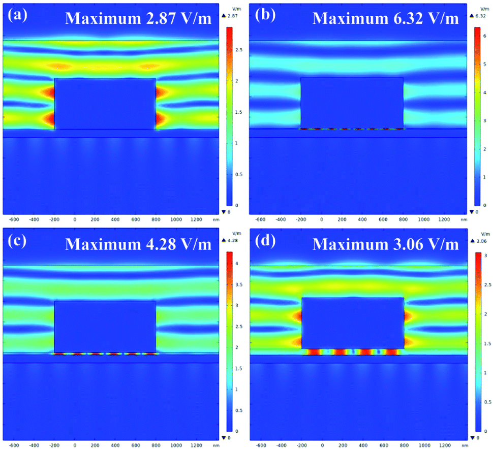
The simulated electric field distributions of four samples have been carried out to study using COMSOL Multiphysics software as shown in Fig. 6. The result demonstrates that the electric field distribution is dispersive and hard to localize for sample A in Fig. 6(a). By contrast, the localization effect of electric field becomes intensive and concentrates on the location between the Ag metal layer and CsPbBr3 perovskite. And the maximum electric field intensity value in the microlaser structure decreases from 6.32 V m−1 to 3.06 V m−1 with increasing the insulator layer SiO2 thickness in Fig. 6(b)–(d), proving that the M–I–S structures can indeed improve the photons of incident light and enhance exciton–photon coupling effect compared with bare Si substrate structure. Moreover, the conclusions of theoretical simulation are very consistent with experimental results as above. However, as the thickness of SiO2 layer increases to 60 nm or over, the electric field intensity value for sample D approaches to sample A (2.87 V m−1), which exhibits that the effect of M–I–S structure begins to become unconspicuous gradually, attributing to that the thickness of SiO2 layer is too thick to trigger the plasmon resonance action. In this situation, it looks that the SiO2 layer should be as thin as possible or even none to obtain stronger exciton–photon coupling effect. It is not the case, if the SiO2 layer is too thin or none, the electric field density increases rapidly, but the metal loss also becomes serious and the lasing modes are unstable as well.18 Referring to our previously published literature,20 the surface plasmon resonance mechanism between CsPbBr3 perovskite and Ag metal film was depicted. It can be found that a large population of excitons is initially excited. Benefiting from existing a near field coupling between the excitons and surface plasmons, here can generate plasmon–exciton-polaritons, which induces relevant quasiparticles in the CsPbBr3-based perovskite laser. Those polaritons then radiate coherently via stimulated relaxation into the plasmonic lasing modes, further providing a faster radiation tunnel by the following expression:38
| | |
1/τcoupled = 1/τnr + 1/τr + 1/τsp ≈ 1/τsp
| (3) |
 |
| | Fig. 6 Simulated electric field distributions and the maximum electric field intensity values of sample (a) A, (b) B, (c) C, and (d) D, respectively. | |
The experimentally determined τcoupled can be described as a Purcell-enhanced spontaneous emission rate (F/τr), where F is the enhancement factor by the Purcell effect.39–43 Purcell effect increases the fraction of polaritons in the plasmonic lasing mode, yielding a lower laser threshold eventually.44–51
Conclusions
In summary, the structures of metal–insulator layers combined with CsPbBr3 perovskite materials were investigated successfully. And results reveal that the thickness of insulator layer of SiO2 and substrate can affect laser generation. Theoretical and experimental results prove that the as-obtained sample B with the thickness of 10 nm SiO2 layer and 80 nm Ag metal film, demonstrates a ultra-low laser threshold as low as 0.138 μW and a high quality (Q) factor of up to 3907, which exhibits the excellent performance compared with the previous reported CsPbBr3 perovskite lasers. It paves the way for the development of high-efficiency CsPbBr3-based micro/nano-lasers and provides fundamental insights for the practical applications of all-inorganic CsPbBr3 perovskite micro-cubes in biomedical, data storage, and on-chip optical communication technologies in the future.
Conflicts of interest
The authors declare no competing financial interests.
Acknowledgements
The authors acknowledge financial support from the National Key Research and Development Program of China (2017YFB0403101), the National Nature Science Foundation of China (62074077, 61921005, 61904068, 61974062), Leading-edge Technology Program of Jiangsu Natural Science Foundation (BK20202005), the Solid-State Lighting and Energy-Saving Electronics Collaborative Innovation Center and the Natural Science Fund of Colleges and Universities in Jiangsu Province (20KJB140024).
References
- R. E. Beal, D. J. Slotcavage, T. Leijtens, A. R. Bowring, R. A. Belisle, W. H. Nguyen, G. F. Burkhard, E. T. Hoke and M. D. McGehee, Cesium Lead Halide Perovskites with Improved Stability for Tandem Solar Cells, J. Phys. Chem. Lett., 2016, 7, 746–751 CrossRef CAS PubMed.
- A. Schlaus, M. Spencer, K. Miyata, F. Liu, X. X. Wang, I. Datta, M. Lipson, A. L. Pan and X. Y. Zhu, How Lasing Happens in CsPbBr3 Perovskite Nanowires, Nat. Commun., 2019, 10, 265 CrossRef PubMed.
- X. Wang, H. Zhou, S. Yuan, W. Zheng, Y. Jiang, X. Zhuang, H. Liu, Q. Zhang, X. Zhu, X. Wang and A. L. Pan, Cesium Lead Halide Perovskite Triangular Nanorods as High-Gain Medium and Effective Cavities for Multiphoton-Pumped Lasing, Nano Res., 2017, 10, 3385–3395 CrossRef CAS.
- Q. Zhang, R. Su, X. Liu, J. Xing, T. C. Sum and Q. H. Xiong, High Quality Whispering-Gallery-Mode Lasing from Cesium Lead Halide Perovskite Nanoplatelets, Adv. Funct. Mater., 2016, 26, 6238–6245 CrossRef CAS.
- Y. Wang, X. Sun, R. Shivanna, Y. Yang, Z. Chen, Y. Guo, G. C. Wang, E. Wertz, F. Deschler and Z. Cai, Photon Transport in One-Dimensional Incommensurately Epitaxial CsPbX3 Arrays, Nano Lett., 2016, 16, 7974 CrossRef CAS PubMed.
- J. Chen, Y. Fu, L. Samad, L. Dang, Y. Zhao, S. Shen, L. Guo and J. Song, Vapor-Phase Epitaxial Growth of Aligned Nanowire Networks of Cesium Lead Halide Perovskites (CsPbX3, X = Cl, Br, I), Nano Lett., 2017, 17, 460 CrossRef CAS PubMed.
- F. Chen, C. X. Xu, Q. Y. Xu, Z. Zhu, F. F. Qin, A. Gowri Manohari and Y. Z. Zhu, Lasing mode evolution and regulation of the perovskite CH3NH3PbBr3, J. Mater. Chem. C, 2017, 5, 9238–9241 RSC.
- Z. Z. Liu, J. Yang, J. Du, Z. P. Hu, T. C. Shi, Z. Y. Zhang, Y. Q. Liu, X. S. Tang, Y. X. Leng and R. X. Li, Robust Subwavelength Single-Mode Perovskite Nanocuboid Laser, ACS Nano, 2018, 12, 5923–5931 CrossRef CAS PubMed.
- F. Chen, C. Zhu, C. X. Xu, P. Fan, F. F. Qin, A. Gowri Manohari, J. F. Lu, Z. L. Shi, Q. Y. Xu and A. L. Pan, Crystal structure and electron transition underlying photoluminescence of methylammonium lead bromide perovskites, J. Mater. Chem. C, 2017, 5, 7739–7745 RSC.
- B. E. Zhou, M. M. Jiang, H. X. Dong, W. H. Zheng, Y. Z. Huang, J. Y. Han, A. L. Pan and L. Zhang, High-Temperature Upconverted Single-Mode Lasing in 3D Fully Inorganic Perovskite Microcubic Cavity, ACS Photonics, 2019, 6, 793–801 CrossRef CAS.
- X. X. Wang, M. Shoaib, X. Wang, X. H. Zhang, M. He, Z. Y. Luo, W. H. Zheng, H. L. Li, T. F. Yang, X. L. Zhu, L. B. Ma and A. L. Pan, High-Quality In-Plane Aligned CsPbX3 Perovskite Nanowire Lasers with Composition-Dependent Strong Exciton-Photon Coupling, ACS Nano, 2018, 12, 6170–6178 CrossRef CAS PubMed.
- Y. G. Zhong, K. Liao, W. N. Du, J. R. Zhu, Q. Y. Shang, F. Zhou, X. X. Wu, X. Y. Sui, J. W. Shi, S. Yue, Q. Wang, Y. F. Zhang, Q. Zhang, X. Y. Hu and X. F. Liu, Large-Scale Thin CsPbBr3 Single-Crystal Film Grown on Sapphire via Chemical Vapor Deposition: Toward Laser Array Application, ACS Nano, 2020, 14, 15605–15615 CrossRef PubMed.
- R. Chen, B. Ling, X. W. Sun and H. D. Sun, Room Temperature Excitonic Whispering Gallery Mode Lasing from High-Quality Hexagonal ZnO Microdisks, Adv. Mater., 2011, 23, 2199–2204 CrossRef CAS PubMed.
- J. C. Johnson, H. J. Choi, K. P. Knutsen, R. D. Schaller, P. Yang and R. J. Saykally, Single Gallium Nitride Nanowire Lasers, Nat. Mater., 2002, 1, 106–110 CrossRef CAS PubMed.
- C. Czekalla, C. Sturm, R. Schmidt-Grund, B. Cao, M. Lorenz and M. Grundmann, Whispering Gallery Mode Lasing in Zinc Oxide Microwires, Appl. Phys. Lett., 2008, 92, 241102 CrossRef.
- M. H. Huang, S. Mao, H. Feick, H. Yan, Y. Wu, H. Kind, E. Weber, R. Russo and P. Yang, Room-Temperature Ultraviolet Nanowire Nanolasers, Science, 2001, 292, 1897–1899 CrossRef CAS PubMed.
- M. S. Gudiksen, L. J. Lauhon, J. Wang, D. C. Smith and C. M. Lieber, Growth of Nanowire Superlattice Structures for Nanoscale Photonics and Electronics, Nature, 2002, 415, 617–620 CrossRef CAS PubMed.
- D. Jiang, B. Liu, T. Tao, T. Zhi, P. Chen, D. J. Chen, Z. L. Xie, X. Q. Xiu, Y. D. Zheng and R. Zhang, The optimization of surface plasmon coupling efficiency in InGaN/GaN nanowire based nanolasers, Appl. Phys. Express, 2020, 13, 085001 CrossRef CAS.
- T. Tao, T. Zhi, B. Liu, J. P. Dai, Z. Zhuang, Z. L. Xie, P. Chen, F. F. Ren, D. J. Chen, Y. D. Zheng and R. Zhang, Manipulable and Hybridized, Ultralow-Threshold Lasing in a Plasmonic Laser Using Elliptical InGaN/GaN Nanorods, Adv. Funct. Mater., 2017, 27, 1703198 CrossRef.
- T. Tao, T. Zhi, B. Liu, P. Chen, Z. L. Xie, H. Zhao, F. F. Ren, D. J. Chen, Y. D. Zheng and R. Zhang, Electron-Beam-Driven III-Nitride Plasmonic Nanolasers in the Deep-UV and Visible Region, Small, 2020, 16, 1906205 CrossRef CAS PubMed.
- R. F. Oulton, V. J. Sorger, D. A. Genov, D. F. P. Pile and X. Zhang, A hybrid plasmonic waveguide for subwavelength confinement and long-range propagation, Nat. Photonics, 2008, 2, 496 CrossRef CAS.
- R. F. Oulton, V. J. Sorger, T. Zentgraf, R. M. Ma, C. Gladden, L. Dai, G. Bartal and X. Zhang, Plasmon lasers at deep subwavelength scale, Nature, 2009, 461, 629 CrossRef CAS PubMed.
- M. I. Stockman and D. J. Bergman, Quantum nanoplasmonics: surface plasmon amplification by stimulated emission of radiation (SPASER), Quantum Electronics & Laser Science. QELS Postconference Digest IEEE, 2003 Search PubMed.
- R. M. Ma and R. F. Oulton, Applications of nanolasers, Nat. Nanotechnol., 2019, 14, 12 CrossRef CAS PubMed.
- M. A. Noginov, G. Zhu, A. M. Belgrave, R. Bakker, V. M. Shalaev, E. E. Narimanov, S. Stout, E. Herz, T. Suteewong and U. Wiesner, Demonstration of a spaser-based nanolaser, Nature, 2009, 460, 1110 CrossRef CAS PubMed.
- R. M. Ma, R. F. Oulton, V. J. Sorger, G. Bartal and X. Zhang, Room-temperature sub-diffraction-limited plasmon laser by total internal reflection, Nat. Mater., 2011, 10, 110 CrossRef CAS PubMed.
- S. Arafin, X. Liu and Z. Mi, Review of recent progress of III-nitride nanowire lasers, J. Nanophotonics, 2013, 7, 074599 CrossRef CAS.
- Z. Han and S. I. Bozhevolnyi, Radiation guiding with surface plasmon polaritons, Rep. Prog. Phys., 2013, 76, 016402 CrossRef PubMed.
- P. J. Cheng, Q. Y. Zheng, C. Y. Hsu, H. Li, K. B. Hong, Y. Z. Zhu, Q. N. Cui, C. X. Xu, T. C. Lu and T. R. Lin, Full-Spectrum Analysis of Perovskite-Based Surface Plasmon Nanolasers, Nanoscale Res. Lett., 2020, 15, 66 CrossRef CAS PubMed.
- H. C. Yu, K. K. Ren, Q. Wu, J. Wang, J. Lin, Z. J. Wang, J. J. Xu, R. F. Oulton, S. C. Qu and P. Jin, Organic-inorganic perovskite plasmonic nanowire lasers with a low threshold and a good thermal stability, Nanoscale, 2016, 8, 19536–19540 RSC.
- Q. Y. Shang, Y. Zhang, Z. Liu, J. Chen, P. F. Yang, C. Li, W. Li, Y. F. Zhang, Q. H. Xiong, X. F. Liu and Q. Zhang, Surface Plasmon Enhanced Strong Exciton-Photon Coupling in Hybrid Inorganic-Organic Perovskite Nanowires, Nano Lett., 2018, 18, 3335–3343 CrossRef CAS PubMed.
- S. W. Eaton, M. Lai, N. A. Gibson, A. B. Wong, L. Dou, J. Ma, L. W. Wang, S. R. Leone and P. Yang, Lasing in robust cesium lead halide perovskite nanowires, Proc. Natl. Acad. Sci. U. S. A., 2016, 113, 1993–1998 CrossRef CAS PubMed.
- H. Zhu, Y. Fu, F. Meng, X. Wu, Z. Gong, Q. Ding, M. V. Gustafsson, M. T. Trinh and X. Y. Zhu, Lead halide perovskite nanowire lasers with low lasing thresholds and high quality factors, Nat. Mater., 2015, 14, 636–642 CrossRef CAS PubMed.
- S. T. Ha, X. F. Liu, Q. Zhang, D. Giovanni, T. C. Sum and Q. H. Xiong, Synthesis of Organic-Inorganic Lead Halide Perovskite Nanoplatelets: Towards High-Performance Perovskite Solar Cells and Optoelectronic Devices, Adv. Opt. Mater., 2014, 2, 838–844 CrossRef CAS.
- Q. Y. Shang, M. L. Li, L. Y. Zhao, D. W. Chen, S. Zhang, S. L. Chen, P. Gao, C. Shen, J. Xing, G. C. Xing, B. Shen, X. F. Liu and Q. Zhang, Role of the Exciton-Polariton in a Continuous-Wave Optically Pumped CsPbBr3 Perovskite Laser, Nano Lett., 2020, 20, 6636–6643 CrossRef CAS PubMed.
- L. Pei, J. S. Zhong, T. Z. Li, W. F. Bai, S. T. Wu, Y. J. Yuan, Y. F. Chen, Z. T. Yu, S. C. Yan and Z. G. Zou, CoS2@N-doped carbon core-shell nanorod array grown on Ni foam for enhanced electrocatalytic water oxidation, J. Mater. Chem. A., 2020, 8, 6795–6803 RSC.
- Z. Liu, Q. Y. Shang, C. Li, L. Y. Zhao, Y. Gao, Q. Li, J. Chen, S. Zhang, X. F. Liu, Y. S. Fu and Q. Zhang, Temperature-dependent photoluminescence and lasing properties of CsPbBr3 nanowires, Appl. Phys. Lett., 2019, 114, 101902 CrossRef.
- A. Yang, T. B. Hoang, M. Dridi, C. Deeb, M. H. Mikkelsen, G. C. Schatz and T. W. Odom, Real-time tunable lasing from plasmonic nanocavity arrays, Nat. Commun., 2015, 6, 6939 CrossRef CAS PubMed.
- R. M. Ma, S. Ota, Y. Li, S. Yang and X. Zhang, Explosives detection in a lasing plasmon nanocavity, Nat. Nanotechnol., 2014, 9, 600 CrossRef CAS PubMed.
- A. González-Tudela, P. A. Huidobro, L. Martín-Moreno, C. Tejedor and F. J. García-Vidal, Theory of strong coupling between quantum emitters and propagating surface plasmons, Phys. Rev. Lett., 2013, 110, 126801 CrossRef PubMed.
- D. Sanvitto and S. Kena-Cohen, The road towards polaritonic devices, Nat. Mater., 2016, 15, 1061–1073 CrossRef CAS PubMed.
- K. Takazawa, J. I. Inoue, K. Mitsuishi and T. Takamasu, Fraction of a millimeter propagation of exciton polaritons in photoexcited nanofibers of organic dye, Phys. Rev. Lett., 2010, 105, 067401 CrossRef PubMed.
- M. Li, Q. Wei, S. K. Muduli, Q. Xu, N. Mathews, S. G. Mhaisalkar, G. Xing and T. C. Sum, Enhanced Exciton and Photon Confinement in Ruddlesden-Popper Perovskite Microplatelets for Highly Stable Low-Threshold Polarized Lasing, Adv. Mater., 2018, 30, 1707235 CrossRef PubMed.
- E. M. Purcell, Spontaneous emission probabilities at radio frequencies, Phys. Rev., 1946, 69, 681 CrossRef.
- F. L. Wang, Y. D. Yang, Y. Z. Huang, Z. X. Xiao and J. L. Xiao, Single-transverse-mode waveguide-coupled deformed hexagonal resonator microlasers, Appl. Opt., 2018, 57, 7242–7248 CrossRef CAS PubMed.
- H. R. Yu, X. Cheng, Y. Wang, Y. Liu, K. Rong, Z. Li, Y. Wan, W. Gong, K. Watanabe and T. Taniguchi, Waterproof Perovskite-Hexagonal Boron Nitride Hybrid Nanolasers with Low Lasing Thresholds and High Operating Temperature, ACS Photonics, 2018, 5, 4520–4528 CrossRef CAS.
- J. Ren, Y. Gu, D. Zhao, F. Zhang, T. Zhang and Q. Gong, Evanescent-Vacuum-Enhanced Photon-Exciton Coupling and Fluorescence Collection, Phys. Rev. Lett., 2017, 118, 073604 CrossRef PubMed.
- S. De Liberato, Light-Matter Decoupling in the Deep Strong Coupling Regime: The Breakdown of the Purcell Effect, Phys. Rev. Lett., 2014, 112, 16401 CrossRef PubMed.
- E. Waks and D. Sridharan, Cavity QED treatment of interactions between a metal nanoparticle and a dipole emitter, Phys. Rev. A: At., Mol., Opt. Phys., 2010, 82, 043845 CrossRef.
- T. Byrnes, N. Y. Kim and Y. Yamamoto, Erratum: Exciton-polariton condensates, Nat. Phys., 2014, 10, 803–813 Search PubMed.
- K. Wang, W. Sun, J. Li, Z. Gu, S. Xiao and Q. Song, Unidirectional Lasing Emissions from CH3NH3PbBr3 Perovskite Microdisks, ACS Photonics, 2016, 3, 1125–1130 Search PubMed.
Footnotes |
| † Electronic supplementary information (ESI) available. See DOI: 10.1039/d1ra06828h |
| ‡ Maogao Gong and Di Jiang contributed equally to this work. |
|
| This journal is © The Royal Society of Chemistry 2021 |
Click here to see how this site uses Cookies. View our privacy policy here. 
 Open Access Article
 This Open Access Article is licensed under a Creative Commons Attribution-Non Commercial 3.0 Unported Licence
 *b,
Chunxiang Xu
*b,
Chunxiang Xu