
 Open Access Article
 This Open Access Article is licensed under a Creative Commons Attribution-Non Commercial 3.0 Unported Licence
Significantly enhanced photoresponse of carbon nanotube films modified with cesium tungsten bronze nanoclusters in the visible to short-wave infrared range
Hao Chena,
Junyi Zhua,
Yang Cao *a,
Jinquan Weib,
Bocheng Lvc,
Qianqian Huc and
Jia-lin Sun*c
*a,
Jinquan Weib,
Bocheng Lvc,
Qianqian Huc and
Jia-lin Sun*c
aSchool of Instrumentation Science and Opto-electronics Engineering, Beijing Information Science &Technology University, Beijing 100192, People's Republic of China. E-mail: caoyang@bistu.edu.cn
bKey Lab for Advanced Materials Processing Technology of Education Ministry, School of Materials Science and Engineering, Tsinghua University, Beijing 100084, People's Republic of China
cCollaborative Innovation Center of Quantum Matter, State Key Laboratory of Low-Dimensional Quantum Physics, Department of Physics, Tsinghua University, Beijing 100084, People's Republic of China. E-mail: jlsun@tsinghua.edu.cn
First published on 13th December 2021
Abstract
Carbon nanotube (CNT) films are promising materials for application in ultra-broadband photodetectors because their absorption range covers the entire spectrum from ultraviolet to the terahertz region, and their detection mechanism is the bolometric effect. Because of the different and limited photothermal conversion efficiencies of CNTs with respect to various wavelengths, the response performance of existing photodetector devices is unsatisfactory, particularly in the infrared band. In this paper, we propose for the first time the use of cesium tungsten bronze (CsxWO3) nanomaterials, which have strong infrared absorption and excellent photothermal conversion properties, to decorate a CNT film for construction of a CsxWO3–CNT composite film photodetector. When compared with CNT-based film photodetectors, the proposed CsxWO3–CNT composite film photodetector shows a significantly enhanced broadband photoresponse over the range from visible light (405 nm) to the short-wave infrared (1550 nm) region, with an average increase in responsivity of 400% and an average increase in specific detectivity of 549%. In addition, the CsxWO3–CNT photodetector shows a fast photoresponse, with a rise time of only 28 ms, which represents a 30% improvement over that of the CNT photodetector. This paper thus provides a new concept for the design of a high-performance broadband photodetector.
1. Introduction
Carbon nanotubes (CNTs) have excellent optical,1,2 electrical,3,4 thermal,5–7 and mechanical8–12 properties. In terms of their photoelectric conversion properties, CNTs represent a promising broadband photoelectric conversion material because of their ability to respond to ultra-wide spectrum light ranging from the ultraviolet (UV) to the terahertz region. Within this range, the photoresponse in the UV region is related to π-plasmon absorption, while the photoresponse in the visible light (VIS) to near-infrared (NIR) region is fundamentally linked to the interband transitions of the CNTs.13–15 When it is extended to the mid-infrared and terahertz regions, the photoresponse is mainly caused by the plasmon resonance that occurs along the main axis of the CNTs.16,17 The entire absorbed light spectrum over the UV to terahertz range can produce heating (with various conversion efficiencies) through electron–phonon interactions.At present, depending on the dominant mechanism, CNT photodetectors can be divided into two main categories. One type of CNT photodetector is based on the photogenerated electron–hole pair separation mechanism, where the photoexcited electron–hole pairs exist in the form of excitons. Because of their one-dimensional structures, CNTs have a strong exciton binding energy, which limits the photogenerated free carrier yield.18 Researchers have made considerable efforts to improve the electron–hole pair separation efficiency in CNTs, with combination of CNTs with other materials to construct various composite structures proving to be an effective method. For example, Wang's group obtained good photoelectric response performance in the VIS to NIR region using ultra-thin single-walled CNT (SWCNT) films that were compounded with graphene.19 Arnold's group obtained a good UV-VIS-NIR response when using semiconductor CNT films compounded with C60.20 However, photodetectors based on the mechanism of photogenerated electron–hole pair separation have an unavoidable drawback, in that the spectral range of their photoresponse is limited by the CNT energy gap, making it impossible to achieve broad-spectrum light detection. Therefore, CNT photodetectors based on this mechanism are mainly focused on detection of VIS and NIR signals.
Another CNT photodetector type is based on the thermal effects caused by the heat generation that occurs after light absorption, including photothermoelectric (PTE) devices and bolometric devices.15,21–23 Among these devices, the bolometer device structure is mainly based on a suspended CNT film, which makes the heat more difficult to dissipate when compared with dissipation from CNTs on a substrate. The heat is mainly transferred through the contact area between adjacent CNTs, which causes a change in the resistance of the CNT-based device. The high thermal conductivity of CNTs forms the basis for the rapid response of this device type.5,24 In 2018, Liu et al. reported an ultra-broadband bolometric photodetector based on suspended CNTs. The effect of the thermal resistance dominates the photoresponse during illumination over the range from UV to the terahertz region.24 However, the device performance is still unsatisfactory, with further improvement required in the infrared (IR) band in particular, and few studies have reported on enhancement of the performance of CNT devices based on the bolometric effect to date.
In recent years, the excellent shielding ability of cesium tungsten bronze nanomaterials in NIR light have made them highly attractive for applications in the photothermal field. Tungsten bronzes are a series of nonstoichiometric compounds with the chemical formula MxWO3 (0 < x < 1), where x is an indeterminate value that can vary from 0 to 1 based on the number of interstitial cations, and M is usually an alkali metal, an ammonium ion, or a rare earth metal ion.25,26 Cesium tungsten bronze (chemical formula: CsxWO3) means that cesium ions (Cs+) are used to dope the tungsten bronze structure. The special internal channel structure and carrier transfer characteristics of this material give it exceptional optical properties. CsxWO3 nanomaterials have high transmittance in the VIS region. Additionally, because of their localized surface plasmon resonance27 and small polariton jumps,28 CsxWO3 nanomaterials also exhibit strong IR absorption over a wide range from 800–2500 nm.29–32 More importantly, these nanocrystals can instantly convert absorbed light energy into thermal energy with high conversion efficiency.33 Therefore, CsxWO3 is an excellent photothermal material.
This paper proposes for the first time that cesium tungsten bronze nanomaterials are used to modify the surfaces of CNT films, and the strong light absorption and high photothermal conversion efficiency of the cesium tungsten bronze nanomaterials are then used to improve the wide-spectrum detection performance of CNTs device significantly via their thermal effect mechanism. In this work, a suspended CNT thin film structure modified with CsxWO3 nanoclusters (CsxWO3–CNT) for a photodetector was fabricated by drop-casting of a CsxWO3 nanosheet dispersion onto a suspended CNT film. The effect of the amount of cesium tungsten bronze used on the detector performance was studied systematically, and the optimal amount of cesium tungsten bronze was determined. When compared with the conventional CNT device, the performance of the CsxWO3–CNT device shows significant improvement. Over the wide spectrum range from the VIS region to the short-wave infrared (SWIR) region (405–1550 nm), the average increase in specific detectivity was 549%, the average increase in responsivity was 400%, and the highest responsivity of 99.65 mA W−1 was achieved at 405 nm (VIS) under 0.625 W irradiation. In terms of response time, the CsxWO3–CNT device exhibits a fast response time of 28 ms, which is 30% faster than the response of the CNT-based device. Cesium tungsten bronze nanocluster modified CNT film detectors are simple to manufacture and offer a new route toward the development of high-performance broadband photodetectors.
2. Experimental
2.1. Preparation and characterization of materials
The CNT films used in this paper were prepared by the floating catalytic chemical vapor deposition (CVD) method.34 Each film has a network structure composed of a mixture of metallic CNTs and semiconducting CNTs and also has a variety of chiral properties,24 thus meaning that the film has a variety of optical and electrical properties. The well-dispersed CsxWO3 nanosheets used in this work were prepared by a water controlled-release process32 and were formulated into an ethanol dispersion with a concentration of 0.78 mg mL−1. The morphologies of both the suspended CNTs and the CsxWO3–CNT composite films were characterized via field emission scanning electron microscopy (FESEM; Hitachi S-4800). The morphology, size, and crystal structure of the CsxWO3 nanomaterials were characterized using transmission electron microscopy (TEM; JEM-2100F, JEOL, Japan). X-ray diffraction (XRD) patterns of the CNT film, the CsxWO3 nanosheets and the CsxWO3–CNT composite film were recorded on a X-ray diffractometer (XRD; Shimadzu XD-1). In order to characterize the thickness of the CNT film, the film is transferred onto a clean silicon wafer, and then ethanol is dropped onto the CNT film surface to make the CNT film closely adhere to the silicon wafer substrate. After the ethanol is dried, the film thickness is measured using an atomic force microscope (AFM; MultiMode 8, Bruker, USA). The absorption spectrum of the CsxWO3 dispersions over the 400–2000 nm wavelength range was measured using a UV-VIS-NIR spectrophotometer (Cary 7000, Agilent, USA). The transmission spectra of the CNT film and the CsxWO3–CNT composite film in the 400–2000 nm wavelength range were recorded using an integrating sphere attachment on the above spectrophotometer.2.2. Fabrication of devices
First, a plexiglass substrate was prepared with a 10 mm-long and 5 mm-wide hollow at its center and it was then cleaned via an ultrasonic cleaning process. Two pieces of carbon conductive tape were cut to lengths of 5 mm and pasted on both ends of the hollow area of the plexiglass substrate. The side of the plexiglass substrate with the conductive adhesive tape was then pressed onto the graphite paper on which the CNT film was grown. Because of the adhesive nature of the conductive tape, a CNT film with the same width as the conductive tape was adhered to the tape and suspended at both ends of the hollow area. In this way, the CNT film that was grown on graphite paper was transferred successfully to a skeletonized plexiglass substrate with a hollowed out center and the suspended CNT film was obtained. Then, a specified volume of the ethanol dispersion of CsxWO3 was drop-cast onto the suspended CNT film surface to obtain the suspended CsxWO3–CNT composite film. After natural drying of the dispersion, gold interdigital electrodes were deposited on the surface of the suspended CNT film and on the side of the CsxWO3–CNT composite film without the CsxWO3 by vacuum thermal evaporation using shadow masks, where these electrodes had a spacing of 200 μm and widths of 200 μm. Finally, the two terminals of the interdigitated electrodes were bonded with copper wires using silver paint to perform the subsequent electrical measurements. The effective working area of the device was 3 mm × 3 mm.2.3. Photoelectric measurements
All tests were performed in a room temperature air environment. The current–voltage (I–V) characteristics and the dynamic optical responses of the CNT devices and the CsxWO3–CNT devices were measured using a Keithley 2400 source meter. VIS irradiation was achieved using a 405 nm laser with a spot diameter of ∼2.5 mm (MDL-III-405; 100 mW) and a 532 nm semiconductor laser with a spot diameter of ∼1.2 mm (MGL-III-532; 200 mW). NIR irradiation was achieved using a 808 nm laser with a spot diameter of ∼3.5 mm (MDL-III-808; 100 mW) and a 1064 nm laser with a spot diameter of ∼1.5 mm (MIL-III-1064; 500 mW). SWIR irradiation was achieved using a 1550 nm laser with a spot diameter of ∼1 mm (MDL-III-1550; 30 mW). All lasers mentioned above were purchased from Changchun New Industries Optoelectronics Technology. All light was incident from the side of the film without any electrodes. The laser spot position on the sample surface was controlled accurately by mounting the samples on a platform with two micrometer calipers that could be adjusted in both the horizontal and vertical directions. The optical power incident on the sample was adjusted using neutral density filters. The turn-on and turn-off operations for the illumination were performed using an electromagnetic shutter (SSH-C2B, OptoSigma). The surface temperature of the device operating area was monitored using an IR thermal imaging camera (DL700, Dali Technology).3. Results and discussion
3.1. Morphology, structure and optical properties of materials
FESEM observations (Fig. 1a) showed that the CNTs are disorderly and are interleaved with each other to form a mesh-like structure. The inset in Fig. 1a shows that the CNT bundles have diameters of 10 to 30 nm and lengths of several micrometers or more,34 indicating that these CNTs have a very large aspect ratio. TEM observations (Fig. 1b) showed that the as-prepared CsxWO3 nanomaterials are formed in sheet-like structures. Fig. 1c shows the crystal structure of these CsxWO3 nanosheets. The lattice spacing of 3.282 Å was identified as that of the (102) crystal plane. The FESEM images (Fig. 1d) show that the reticular structure of the CNT film remained unchanged after drop-casting of the CsxWO3 nanosheet ethanol dispersion. The CsxWO3 nanosheets aggregated into clusters with sizes ranging from 100 nm up to several hundred nanometers; these clusters were dispersed uniformly within the CNT network, thus forming a well-distributed CsxWO3–CNT composite film system.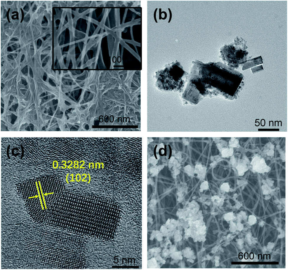 | ||
| Fig. 1 (a) FESEM image of CNT films with low resolution, with a high resolution image shown in the inset. TEM images of CsxWO3 nanosheets with (b) low resolution and (c) high resolution. (d) FESEM image of the CsxWO3–CNT composite film. | ||
The crystal structure of the CNT film, the CsxWO3 nanosheets and the CsxWO3–CNT composite film were further characterized by XRD diffraction analysis. As shown in Fig. 2, black curve shows the XRD pattern of the CsxWO3 nanosheets. All peaks could be indexed to the hexagonal cesium tungsten bronze (JCPDS no. 831334), which indicates that x value of is 0.32 in the CsxWO3 molecular formula. Blue curve shows the XRD pattern of the CNT film. The broad diffraction peaks were observed at 2θ of 14.1°, 29.5° and 43.4°. Red curve shows the XRD pattern of the CsxWO3–CNT composite film. It is composed of the broad diffraction peaks of CNT and the sharp diffraction peaks of CsxWO3, which indicates that CsxWO3 and CNT in the CsxWO3–CNT composite film remain the individual phase and crystallite properties.
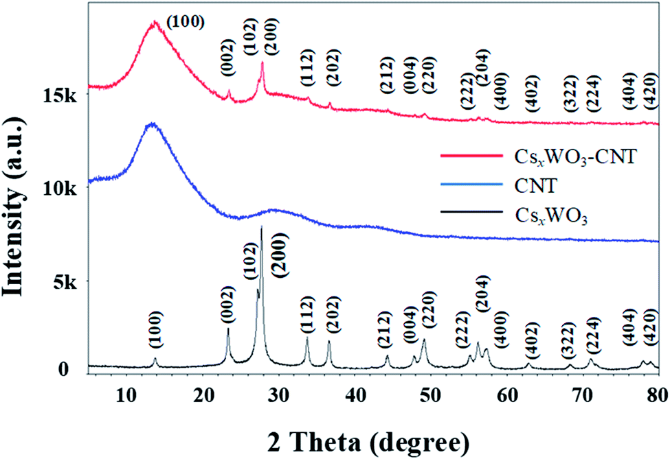 | ||
| Fig. 2 XRD patterns of CNT film, CsxWO3 nanosheets and CsxWO3–CNT composite film (reference: Cs0.32WO3, JCPDS no. 831334). | ||
The results of AFM measurements of the CNT film are shown in Fig. 3. Fig. 3a shows that the silicon substrate region and the CNT film region can be clearly distinguished. Fig. 3b shows the silicon wafer region is flat, while the height of the CNT film region is obviously fluctuating due to the network structure of the CNT film. The average thickness of the CNT film is 88.5 nm.
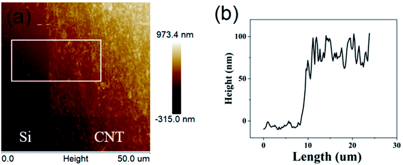 | ||
| Fig. 3 (a) The AFM image of CNT film on silicon wafer substrate (b) The height profile corresponds to the white rectangular box region in (a). | ||
In addition, the optical properties of the CsxWO3 nanosheet ethanol dispersion, the CNT film, and the CsxWO3–CNT composite film were characterized. Fig. 4a shows the absorption spectrum of the dispersion of the CsxWO3 nanosheets, which indicates that CsxWO3 has strong light absorption in the IR band from 800–2000 nm, with an average absorbance of 46%. Because both the CNT film and the CsxWO3–CNT composite film are reticular and thin (and almost semitransparent), the two films hardly reflect any light. Therefore, the absorbances of these films can be calculated using the following equation:
| A = 100% − T | (1) |
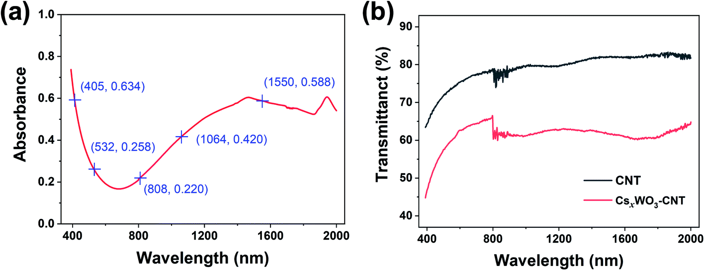 | ||
| Fig. 4 (a) Absorbance spectrum of CsxWO3 nanosheet dispersion. (b) Transmittance spectra of a suspended CNT film and a CsxWO3–CNT composite film. | ||
3.2. Photoresponses of the devices
As shown in Fig. 5, a fully suspended CNT thin film device (Fig. 5a) and a CsxWO3–CNT composite thin film device (Fig. 5b) were prepared based on a suspended CNT film and a CNT film modified with CsxWO3 nanoclusters, respectively, which will be referred to as the CNT device and the CsxWO3–CNT device, and the insets show the cross-sectional structures of the two films.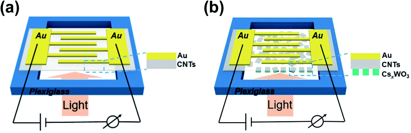 | ||
| Fig. 5 Diagrams of (a) suspended CNT device and (b) suspended CsxWO3–CNT device. The local cross-sections of the thin films are also shown. | ||
To obtain the best possible performance from the CsxWO3–CNT device, the effect of the amount of CsxWO3 present on the photocurrent of the CsxWO3–CNT device was studied systematically. The light current (Ilight) and the dark current (Idark) are defined as the steady-state currents of the device under illumination and in the dark, respectively. The photocurrent (Iph) is defined as the difference between |Ilight| and |Idark|, i.e., Iph = |Ilight| − |Idark|. The CsxWO3 nanosheet ethanol dispersion with a concentration 0.78 mg mL−1 was drop-cast onto the CNTs film, with a volume of 5 μL being applied each time, and was allowed to dry naturally for 10 min before the Iph of the device was tested. The drop-casting process above was repeated 16 times to increase the amount of CsxWO3 on the CNT film surface from 0 μL to 80 μL. The Iph values of the CsxWO3–CNT device for each different amount of CsxWO3 were measured separately, and the relationship between the CsxWO3 dosage and the Iph of the device was finally obtained; the results are shown in Fig. 6. When the amount of CsxWO3 is in the 30–40 μL range, the Iph of the device reaches its highest value, and as the amount of CsxWO3 added continues to increase, the Iph of the device then starts to decrease. This may be because the continued increase in the amount of CsxWO3 causes the agglomeration of the CsxWO3 nanosheets to become more severe, thus resulting in a continued increase in the size of the formed CsxWO3 clusters. This would mean that the heat generated by light absorption in each CsxWO3 cluster can only be transferred within the cluster itself and the heat cannot be conducted via contact to the CNTs, which then leads to the reduced device Iph. Therefore, for the later study, the optimal volume of 35 μL of the CsxWO3 nanosheet dispersion was used to modify the CNT film.
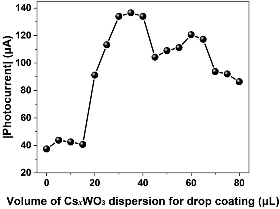 | ||
| Fig. 6 Photocurrent as a function of the volume of the CsxWO3 dispersion drop-coated on the CNT film surface under laser illumination at 532 nm of 2 mW under a bias voltage of −0.5 V. | ||
The I–V characteristics of the CNT device and the CsxWO3–CNT device in the dark and under light illumination are shown in Fig. 7. Regardless of the size of the positive bias voltage interval or the negative bias voltage interval within the bias voltage range from −0.8 V to +0.8 V, the absolute value of Ilight is always lower than the absolute value of Idark, which shows that the device resistance under illumination is greater than that in the dark, i.e., the illumination causes an increase in the device resistance. The I–V characteristics of the two devices are linearly fitted over a bias voltage range of −0.1 V to +0.1 V, and the linearly fitted straight lines were extended to the entire bias voltage range, as shown by the dotted line in Fig. 7. It can be seen that the I–V characteristics are not strictly linear, but have weak nonlinearity, indicating that the CNT film is composed of metallic CNTs and semiconducting CNTs, and the metallic CNTs is dominant.
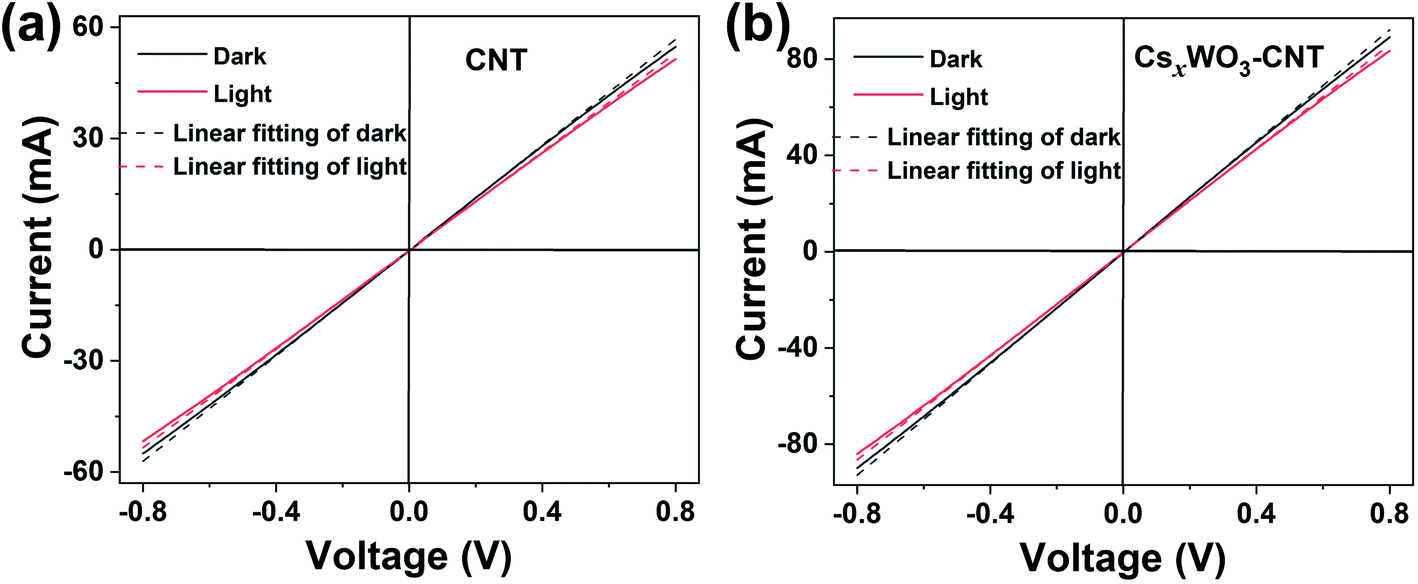 | ||
| Fig. 7 The solid lines are the I–V characteristics of (a) CNT device and (b) CsxWO3–CNT device under dark conditions and under VIS irradiation at 532 nm (7.5 mW). The dotted lines are extensions of the linear fitting in the range of −0.1 V to 0.1 V. | ||
The photoresponses of the CNT device and the CsxWO3–CNT device under on-off light modulation at various wavelengths are shown in Fig. 8. When the laser irradiates the devices, the photocurrent begins to increase rapidly in the negative direction until it reaches a stable value. When the laser is turned off, the photocurrent then decreases rapidly and returns to 0 mA. The most striking result here is that the photocurrents of the CsxWO3–CNT devices are much higher than those of the CNT devices over the wide spectral range from the VIS to SWIR (405–1550 nm) regions under the same measurement conditions. These results show that the combination of the CsxWO3 nanoclusters and the CNTs can enhance the photoresponses of the resulting devices significantly. Furthermore, the photoresponse mechanism can be understood from the data shown in Fig. 8. Regardless of the wavelength of the incident light (i.e., of the energy of the photon), both devices show a negative photocurrent. This phenomenon again confirms that the absolute value of Ilight is smaller than the absolute value of Idark, which is consistent with the results of measurement of the I–V characteristics. This reveals that the dominant mechanism in the photoresponse is the increase in device resistance caused by heat generation after absorption of the photon energy, i.e., the bolometric effect.
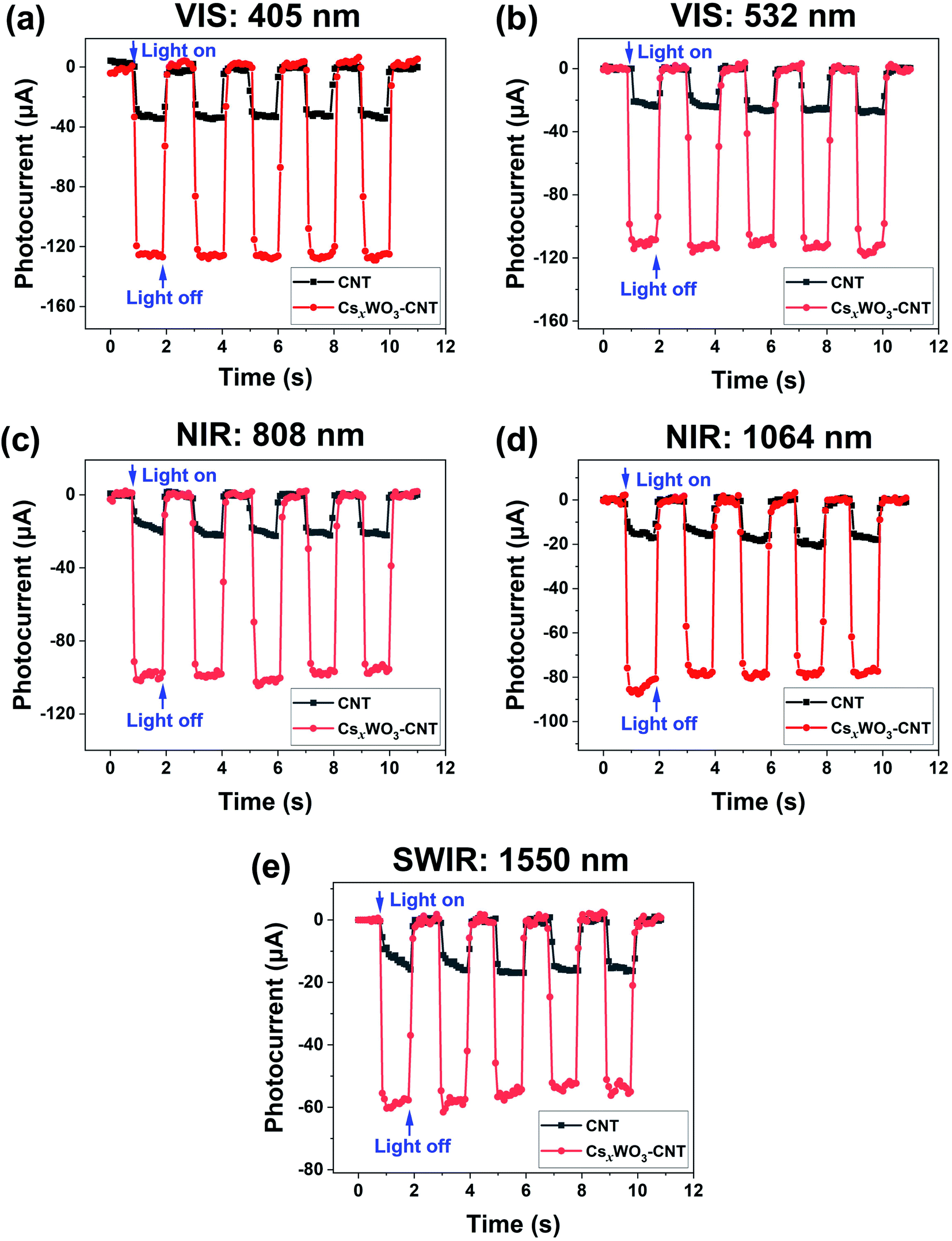 | ||
| Fig. 8 Photoresponses of the CNT device and the CsxWO3–CNT device under a bias voltage of −0.5 V. The incident laser wavelengths are (a) 405 nm (VIS), (b) 532 nm (VIS), (c) 808 nm (NIR), (d) 1064 nm (NIR), and (e) 1550 nm (SWIR), where all incident beams have an optical power of approximately 1.4 mW. | ||
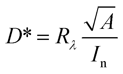
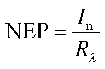
The responsivity (Rλ) is an important parameter for photodetectors and is defined as the photocurrent generated per unit power of the incident light. The responsivities of the CNT device and the CsxWO3–CNT device under illumination at various wavelengths were calculated and the results are shown in Table 1. These results show that the responsivity of the CsxWO3–CNT device is several times higher than that of the CNT device, and the average increase in responsivity was 400% over a wide spectral range from the VIS to the SWIR region (405–1550 nm). For the CsxWO3–CNT device, the highest responsivity of 99.65 mA W−1 was achieved under irradiation with a power of 0.625 W at 405 nm (VIS) (see Fig. 9). The dominant mechanism in the photoresponse for both the CsxWO3–CNT device and the CNT device is the bolometric effect. For the CNT device, the heat only comes from the light-to-heat conversion that occurs after the CNT film absorbs the light, while for the CsxWO3–CNT device, the heat comes from the light-to-heat conversion process that occurs after the CsxWO3 and the CNT film both absorb light. Of these materials, the CsxWO3 nanocrystals can convert the absorbed photo-energy into local heat instantaneously with high conversion efficiency,33,34 and the photothermal conversion efficiency of these nanocrystals is significantly higher than that of the CNT film (see Fig. 11 below and the related discussion). Therefore, the performance of the CsxWO3–CNT device is a significant improvement over that of the CNT device.
| Wavelength (nm) | CNT device | CsxWO3–CNT device | ||||||
|---|---|---|---|---|---|---|---|---|
| Rλ (mA W−1) |
|
NEP (10−6 W Hz−1/2) | D* (106 Jones) | Rλ (mA W−1) |
|
NEP (10−6 W Hz−1/2) | D* (106 Jones) | |
| 405 | 22.10 | 7.48 | 96.12 | 3.12 | 90.14 | 30.52 | 17.71 | 16.9 |
| 532 | 18.20 | 16.10 | 116.72 | 2.57 | 78.10 | 69.09 | 20.44 | 14.7 |
| 808 | 15.34 | 1.60 | 138.48 | 2.17 | 70.20 | 7.30 | 22.74 | 13.2 |
| 1064 | 13.25 | 7.50 | 160.33 | 1.87 | 56.30 | 31.88 | 28.36 | 10.6 |
| 1550 | 11.54 | 14.70 | 184.09 | 1.63 | 39.50 | 50.32 | 40.42 | 7.4 |


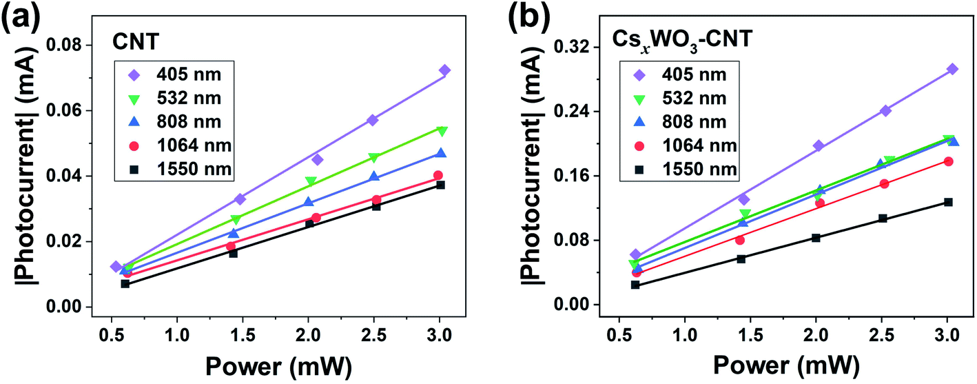 | ||
| Fig. 9 Absolute value of photocurrent versus incident optical power for (a) CNT device and (b) CsxWO3–CNT device. The optical power is approximately 1.4 mW at wavelengths of 405 nm (VIS), 532 nm (VIS), 808 nm (NIR), 1064 nm (NIR), and 1550 nm (SWIR), all under a bias voltage of −0.5 V. | ||
An in-depth evaluation and analysis of the spectral performance of the CsxWO3–CNT device is very important for application of the device. However, the laser spot area is different at each wavelength and the spot area for most wavelengths is smaller than the effective working area of the device. Therefore, to compare the performances of the CsxWO3–CNT device at various wavelengths quantitatively, we also calculated the responsivity per unit spot area for each irradiation wavelength; this quantity is defined as 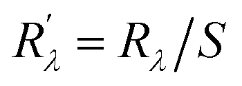 , where Rλ and S are the responsivity and the spot area of the laser, respectively. All these results are summarized in Table 1.
The highest 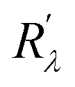 value of the CsxWO3–CNT device occurs at a wavelength of 532 nm. This is because the CNTs can provide their greatest thermal contribution to the CsxWO3–CNT device at this wavelength. In the CNTs, the electrons that are excited by irradiation at 532 nm will all be de-excited in a nonradiative manner, while the de-excitation process in the other bands occurs in both photoemissive and nonradiative ways,35 indicating that the CNTs have their highest thermal conversion efficiency at 532 nm. In addition, the second highest and third highest
  values appear at wavelengths of 1550 and 1064 nm, respectively. This is mainly because of the high absorbance (see Fig. 2a) and the excellent photothermal conversion efficiency of the CsxWO3 nanomaterials in the IR band. Furthermore, in the IR band (at 808, 1064, and 1550 nm),
  continues to increase as the wavelength increases, which is mainly related to the higher absorbance property of CsxWO3 at longer wavelengths, as Fig. 2a illustrates.
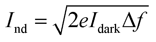
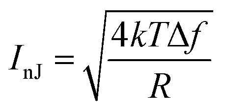
A Source Meter unit Keithley 2400 was used to obtain Idark signal as a function of time. The bias voltage is −0.5 V same as the value applied when detecting the Ilight. The recorded Idark data was then converted to noise power spectral density using Fourier transformation. The square root of the noise power spectral density is the noise current spectral density. The total noise of the CNT device and the CsxWO3–CNT device are 2.12 × 10⁻⁶ A Hz−1/2 and 1.60 × 10⁻⁶ A Hz−1/2 at a bandwidth of 1 Hz, respectively. This total noise value includes thermal noise, shot noise, and 1/f noise. Among them, the shot noise Ind can be calculated according to the following formula.
 | (2) |
 | (3) |
 | (4) |
 | (5) |
Fig. 9 shows that the photocurrents of both the CNT device and the CsxWO3–CNT device are strongly proportional to the incident laser power within the range from 530 μW to 3 mW. The linear power detection range extends from microwatt to milliwatt levels, and can even be extended further to higher powers. This shows that the device is suitable for quantitative light detection applications.
The response speed is also an important parameter for photodetectors. The rise time and the decay time of the photodetector represent the time gaps between 10% and 90% of the photocurrent peak values at the rising and falling edges, respectively. We calculated the response times of the two devices to irradiation of 3 mW at 532 nm. As shown in Fig. 10, the rise/fall times of the CNT photodetector are 41 ms/55 ms, and the rise/fall times of the CsxWO3–CNT photodetector are 28 ms/42 ms. When compared with the CNT devices, the response time of the CsxWO3–CNT photodetector is reduced significantly by 13 ms, and the response speed is improved by 30%. These fast device responses can be attributed to the ultra-high thermal conductivity of the CNTs, which also ensures that the CNTs can achieve rapid warming and cooling.5 Corresponding to this high thermal conductivity, the CNTs also have a low specific heat capacity,37 which allows the CNTs to change the film temperature rapidly when heated, meaning that all our devices show fast responses. In addition, the response speed of the CsxWO3–CNT device is better than that of the CNT device. This higher response speed may be due to the CsxWO3 nanocrystals having better dynamic characteristics during the heating and cooling processes than the CNTs.
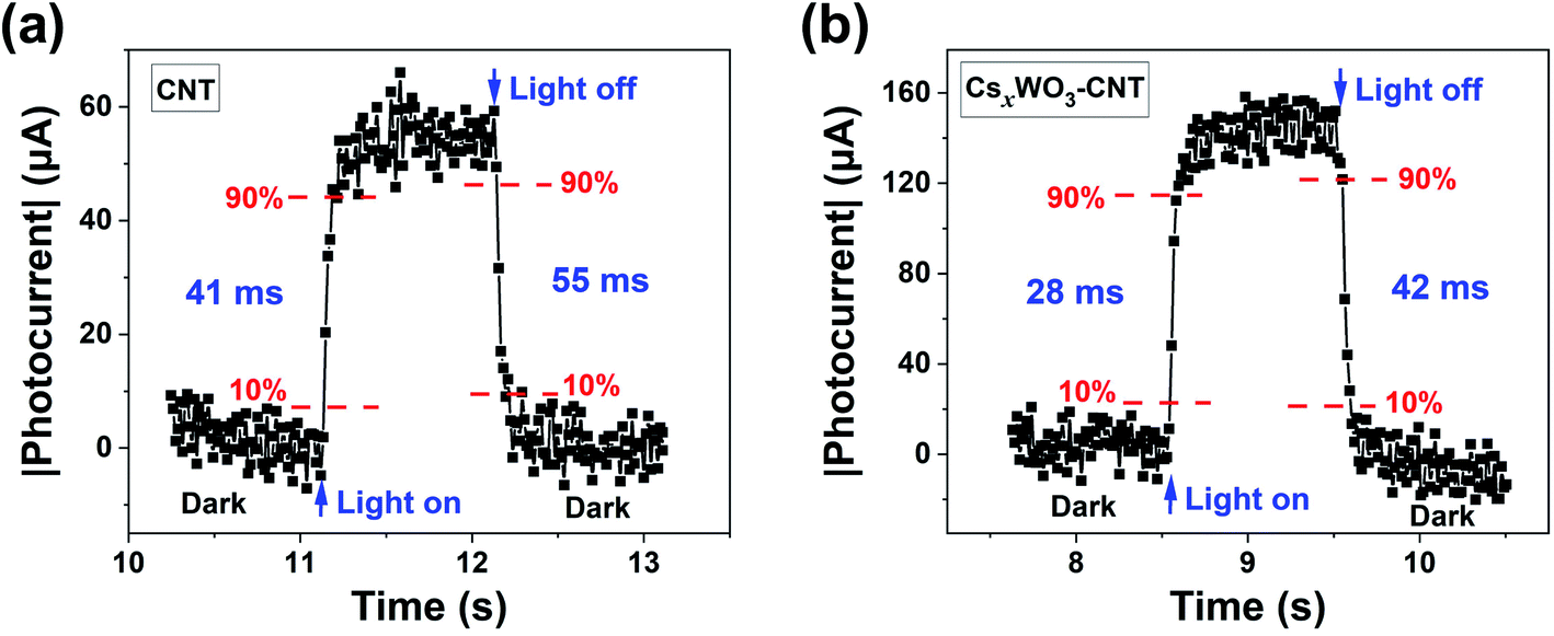 | ||
| Fig. 10 Enlarged plots of individual on/off characteristics of (a) CNT device and (b) CsxWO3–CNT device photoresponses under 532 nm irradiation with optical power of 3 mW at a bias voltage of −0.5 V. | ||
The surface temperatures of the CNT device and the CsxWO3–CNT device in the working area under the light and dark state conditions were captured using an infrared thermal imaging camera, and the results are shown in Fig. 11. Under 1064 nm NIR light illumination, both devices showed a temperature increase. For the CNT device, the temperature in the irradiated area increased to 34.4 °C from the dark state temperature of 32.8 °C. The temperature increment is thus 1.6 °C. However, for the CsxWO3–CNT device, after irradiation for the same time duration, the temperature in the irradiated area increased to 38.3 °C from the dark state temperature of 32.9 °C. This temperature increment thus reached 5.4 °C. The figures show that there is basically no difference in temperature between the two devices in the dark state, but the surface temperature of the effective working region of the CsxWO3–CNT device is approximately 4 °C higher than that of the CNT device under the same illumination conditions. In the CsxWO3 crystal structure, the Cs+ doping and the formation of oxygen vacancies can produce large numbers of free electrons, and these free electrons will undergo reciprocal motion and generate oscillations under the action of the applied electromagnetic field. When the oscillation frequency is close to the frequency of the electromagnetic field, the structure will resonate, and incident light with the resonance frequency will be absorbed and converted into vibrational energy. In addition, because of the injection of Cs+, the carriers in CsxWO3 are bound to the tungsten position and they polarize the surrounding lattice to form small polaritons, which absorb the infrared light when it jumps between the W5+ and W6+ positions. Under the combined action of the local surface plasmon resonance and the small polariton hopping, the CsxWO3 nanoclusters produce strong infrared absorption. When coupled with excellent photothermal conversion efficiency of CsxWO3, this leads to a significant temperature increase in the CsxWO3–CNT composite film.
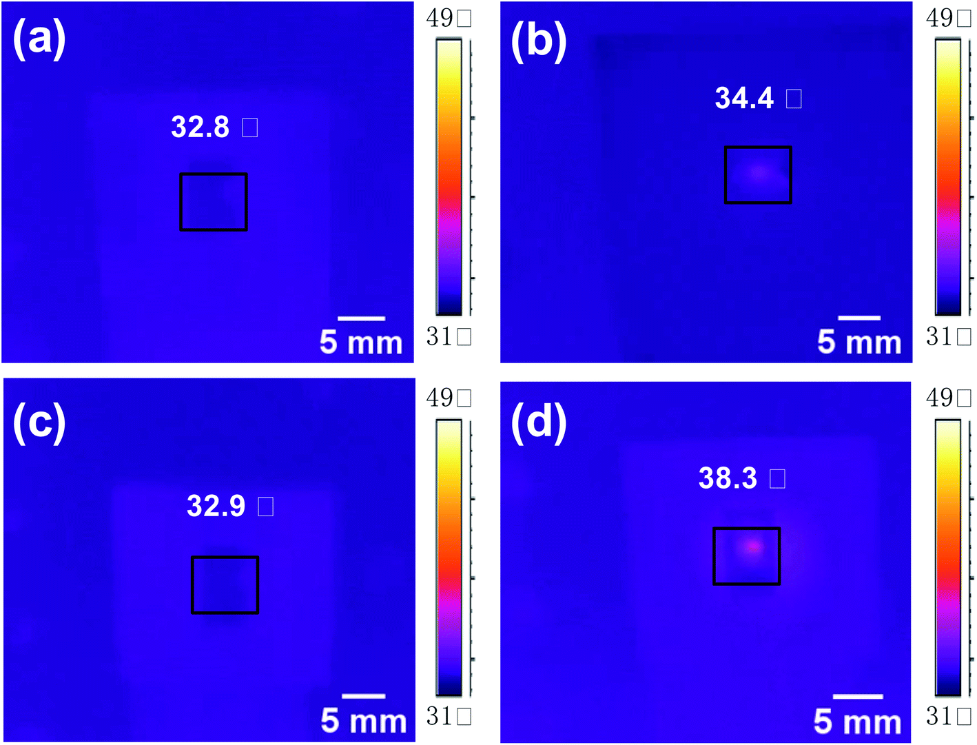 | ||
| Fig. 11 Thermal images of (a and b) the CNT device and (c and d) the CsxWO3–CNT device acquired by infrared thermography under identical conditions, where (a) and (c) were in the dark state and (b) and (d) were under illumination at 1064 nm (NIR) with optical power of 25.20 mW. | ||
All the important parameters (i.e., the responsivity, the response time, and D*) of the CsxWO3–CNT photodetector are summarized and are compared with the corresponding parameters of other representative reported photodetectors with a bolometric effect-based mechanism, as shown in Table 2. These results show that our suspended CsxWO3–CNT photodetector provides a broad-spectrum response, high detectivity, and good performance, thus demonstrating its promise for use in high-efficiency photodetection applications.
| Material | Wavelength (μm) | Highest responsivity | Response time | Highest D* (cm Hz1/2 W−1) | Ref. |
|---|---|---|---|---|---|
| Suspended SWCNTs (patterned Si) | 1–1.3 | 250 V W−1 | 40–60 ms | 4.5 × 10⁵ | 38 |
| Suspended MWCNTs (patterned Si) | 1–1.3 | N/A | 1–2 ms | 3.3 × 10⁶ | 39 |
| Aligned SWCNTs (PVP matrix) | 0.3–2 | 230 V W−1 | 0.94 ms | 1.2 × 10⁸ | 40 |
| Suspended MWCNTs (Ag antennas) | 10.6 | 800 V W−1 | 25 ms | 1 × 10⁷ | 41 |
| Suspended aligned SWCNTs (polystyrene matrix) | 2.5–20 | 500 V W−1 | 150–200 ms | N/A | 42 |
| Suspended SWCNTs (PNIPAm matrix) | 1–20 | 48 V W−1 | 83 ms | N/A | 43 |
| DWCNT film (SiO2/Si substrate) | 1–1.3 | 5 × 10⁴ V W−1 | 1.5–2 ms | 2 × 10⁷ | 44 |
| Suspended MWCNTs | 0.94 | 110 V W−1 | 750 ms | 4 × 10⁶ | 45 |
| Suspended CNTs | 0.375–118.8 | 50.9 mA W−1 | 70 ms | 3.5 × 10⁷ | 24 |
| Suspended CsxWO3–CNTs | 0.405–1.550 | 99.65 mA W−1 | 28 ms | 1.69 × 10⁷ | This work |
4. Conclusions
In summary, we prepared two types of photodetector based on a CNT thin film and a CsxWO3–CNT composite film. We then compared the photodetection performances of these two devices over a wide spectral range from the VIS region (405 nm) to the SWIR region (1550 nm). The results showed that the modification provided by the CsxWO3 nanoclusters on the surface of the CNT film could enhance the light absorption of these films, particularly in the IR band (800–2000 nm). In the CsxWO3–CNT device, the strong light absorption ability and efficient photothermal conversion property of CsxWO3 complement the photoresponse based on the bolometric effect of the CNTs, thus significantly improving the device performance. When compared with the CNT devices, the CsxWO3–CNT device shows average increases of 400% in responsivity and 549% in specific detectivity over the broad spectral range from the VIS region (405 nm) to the SWIR region (1550 nm), in which the detection performance at 808 nm (NIR) has shown the greatest improvement, with a 609% increase in specific detectivity. In addition, the response speed of the CsxWO3–CNT device is improved by 30% when compared with the CNT device. These results show that CNTs modified with CsxWO3 nanoclusters represent a promising composite material. Nanomaterials with significant photothermal effects can be used to improve the performances of photodetectors with a bolometric effect-based mechanism. This therefore provides a new route toward the development of uncooled high-performance broadband photodetectors. The finding has great significance in the development of optical nanomaterials, broadband photodetector technology and photothermal therapy.Conflicts of interest
There are no conflicts to declare.Acknowledgements
This work was supported by Beijing Municipal Natural Science Foundation (no. 4192024) and National Natural Science Foundation of China (51972188).References
- S. Imtiaz, M. Siddiq, A. Kausar, S. T. Muntha, J. Ambreen and I. Bibi, Chin. J. Polym. Sci., 2018, 4, 445–461 CrossRef.
- Y. R. Poudel and W. Li, Mater. Today Phys., 2018, 7, 7–34 CrossRef.
- J. W. G. Wilder, L. C. Venema, A. G. Rinzler, R. E. Smalley and C. Dekker, Nature, 1998, 391, 59–62 CrossRef.
- M. Kociak, A. Y. Kasumov, S. Guéron, B. Reulet and H. Bouchiat, Phys. Rev. Lett., 2003, 329, 1321–1322 Search PubMed.
- S. Berber, Y. K. Kwon and D. Tomanek, Phys. Rev. Lett., 2000, 84, 4613–4616 CrossRef CAS PubMed.
- A. Yu, P. Ramesh, X. Sun, E. Bekyarova, M. E. Itkis and R. C. Haddon, Adv. Mater., 2008, 20, 4740–4744 CrossRef CAS.
- J. Hone, M. Whitney, C. Piskoti and A. Zettl, Phys. Rev. B: Condens. Matter Mater. Phys., 1999, 59, 2514–2516 CrossRef.
- M. S. Dresselhaus, G. Dreseelhaus and P. C. Eklund, Science of Fullerenes and Carbon Nanotubes, 1996 Search PubMed.
- N. Yao and V. Lordi, J. Appl. Phys., 1998, 84, 1939–1943 CrossRef CAS.
- B. G. Demczyk, Y. M. Wang, J. Cumings, M. Hetman, W. Han, A. Zettl and R. O. Ritchie, Mater. Sci. Eng., A, 2002, 334, 173–178 CrossRef.
- K. Mylvaganam and L. C. Zhang, Carbon, 2004, 42, 2025–2032 CrossRef CAS.
- M. F. Yu, O. Lourie, M. J. Dyer, K. Moloni, T. F. Kelly and R. S. Ruoffl, Science, 2000, 287, 637–640 CrossRef CAS PubMed.
- T. Pichler, M. Knupfer, M. S. Golden, J. Fink and R. E. Smalley, Phys. Rev. Lett., 1998, 80, 4729–4732 CrossRef CAS.
- M. E. Itkis, S. Niyogi, M. E. Meng, M. A. Hamon, H. Hu and R. C. Haddon, Nano Lett., 2002, 2, 155–159 CrossRef CAS.
- M. E. Itkis, F. Borondics, A. Yu and R. C. Haddon, Science, 2006, 312, 413–416 CrossRef CAS PubMed.
- Q. Zhang, E. H. Hároz, Z. Jin, L. Ren, X. Wang, R. S. Arvidson, A. Lüttge and J. Kono, Nano Lett., 2013, 13, 5991–5996 CrossRef CAS PubMed.
- K. C. Chiu, A. L. Falk, P. H. Ho, D. B. Farmer and S. J. Han, Nano Lett., 2017, 17, 5641–5645 CrossRef CAS PubMed.
- A. Fujiwara, Y. Matsuoka, H. Suematsu, N. Ogawa and Y. Achiba, Nanonetwork Materials, 2001, vol. 590, pp. 35–44 Search PubMed.
- Y. Liu, F. Wang, X. Wang, X. Wang, E. Flahaut, X. Liu, Y. Li, X. Wang, Y. Xu, Y. Shi and R. Zhang, Nat. Commun., 2015, 6, 8589 CrossRef CAS PubMed.
- M. S. Arnold, J. D. Zimmerman, C. K. Renshaw, X. Xu and S. R. Forrest, Nano Lett., 2009, 9, 3354–3358 CrossRef CAS PubMed.
- X. He, N. Fujimura, J. M. Lloyd, K. J. Erickson, A. A. Talin, Q. Zhang, W. Gao, Q. Jiang, Y. Kawano and R. H. Hauge, Nano Lett., 2014, 14, 3953–3958 CrossRef CAS PubMed.
- S. Nanot, A. W. Cummings, C. L. Pint, A. Ikeuchi and J. Kono, Sci. Rep., 2013, 3, 1335 CrossRef PubMed.
- M. Mahjouri-Samani, Y. S. Zhou, X. N. He, W. Xiong, P. Hilger and Y. F. Lu, Nanotechnology, 2012, 24, 035502 CrossRef PubMed.
- Y. Liu, J. Yin, P. Wang, Q. Hu, Y. Wang, Y. Xie, Z. Zhao, Z. Dong, J. L. Zhu and W. Chu, ACS Appl. Mater. Interfaces, 2018, 10, 36304–36311 CrossRef CAS PubMed.
- O. Zivkovic, C. Yan and M. J. Wagner, J. Mater. Chem., 2009, 19, 6029–6033 RSC.
- L. Chen, S. Lam, Q. Zeng, R. Amal and A. Yu, J. Phys. Chem. C, 2012, 116, 11722–11727 CrossRef CAS.
- K. A. Willets and R. V. Duyne, Annu. Rev. Phys. Chem., 2007, 58, 267–297 CrossRef CAS PubMed.
- K. Adachi and T. Asahi, J. Mater. Res., 2012, 27, 965–970 CrossRef CAS.
- C. Guo, S. Yin, H. Yu, S. Liu, Q. Dong, T. Goto, Z. Zhang, Y. Li and T. Sato, Nanoscale, 2013, 5, 6469–6478 RSC.
- Z. Yu, Y. Yao, J. Yao, L. Zhang, Z. Chen, Y. Gao and H. Luo, J. Mater. Chem. A, 2017, 5, 6019–6024 RSC.
- A. A. Tessema, C. M. Wu, K. G. Motora and S. Naseem, Compos. Sci. Technol., 2021, 211, 108865 CrossRef CAS.
- C. Guo, S. Yin, M. Yan and T. Sato, J. Mater. Chem., 2011, 21, 5099–5105 RSC.
- C. Guo, S. Yin, L. Huang and S. T. Yang, Chem. Commun., 2011, 47, 8853–8855 RSC.
- Z. Li, Y. Jia, J. Wei, K. Wang, Q. Shu, X. Gui, H. Zhu, A. Cao and D. Wu, J. Mater. Chem., 2010, 20, 7236–7240 RSC.
- S. M. Bachilo, M. S. Strano, C. Kittrell, R. H. Hauge, R. E. Smalley and R. B. Weisman, Science, 2002, 298, 2361–2366 CrossRef CAS PubMed.
- S. Park, S. J. Kim, J. H. Nam, G. Pitner, T. H. Lee, A. L. Ayzner, H. L. Wang, S. W. Fong, M. Vosgueritchian, Y. J. Park, M. L. Brongersma and Z. N. Bao, Adv. Mater., 2015, 27, 759–765 CrossRef CAS PubMed.
- L. X. Benedict, S. G. Louie and M. L. Cohen, Solid State Commun., 1996, 100, 177–180 CrossRef CAS.
- R. Lu, Z. Li, G. Xu and J. Z. Wu, Appl. Phys. Lett., 2009, 94, 163110 CrossRef.
- F. J. Baca, J. J. Shi, J. Z. Wu and R. Lu, J. Appl. Phys., 2010, 108, 084305 CrossRef.
- G. Vera-Reveles, T. J. Simmons, M. Bravo-SaNchez, M. A. Vidal, H. Navarro-Contreras and F. J. GonzaLez, ACS Appl. Mater. Interfaces, 2011, 3, 3200–3204 CrossRef CAS PubMed.
- M. Mahjouri-Samani, Y. S. Zhou, X. N. He, W. Xiong, P. Hilger and Y. F. Lu, Nanotechnology, 2012, 24, 035502 CrossRef PubMed.
- A. Y. Glamazda, V. A. Karachevtsev, W. B. Euler and I. A. Levitsky, Adv. Funct. Mater., 2012, 22, 2177–2186 CrossRef CAS.
- G. E. Fernandes, H. K. Jin, A. K. Sood and J. Xu, Adv. Funct. Mater., 2013, 23, 4678–4683 CAS.
- C. Christianson, R. Lu and J. Wu, Nanotechnology, 2014, 25, 425503 CrossRef PubMed.
- J. John, M. Muthee, M. Yogeesh, S. K. Yngvesson and K. R. Carter, Adv. Opt. Mater., 2014, 2, 581–587 CrossRef CAS.
| This journal is © The Royal Society of Chemistry 2021 |