
 Open Access Article
 This Open Access Article is licensed under a Creative Commons Attribution-Non Commercial 3.0 Unported Licence
Layered Si–Ti oxide thin films with tailored electrical and optical properties by catalytic tandem MLD-ALD†
Boaz Kalderona,
Debabrata Sarkar b,
Krushnamurty Killia,
Tamuz Danzigc,
Doron Azulayc,
Oded Milloc,
Gili Cohen-Tagurid and
Roie Yerushalmi*a
b,
Krushnamurty Killia,
Tamuz Danzigc,
Doron Azulayc,
Oded Milloc,
Gili Cohen-Tagurid and
Roie Yerushalmi*a
aInstitute of Chemistry, The Center for Nanoscience and Nanotechnology, The Hebrew University of Jerusalem, Edmond J. Safra Campus, Givat Ram, Jerusalem, 91904, Israel. E-mail: roie.yerushalmi@mail.huji.ac.il
bApplied NanoPhysics Laboratory, Department of Physics and Nanotechnology, SRM Institute of Science and Technology, Kattankulathur, 603203, India
cRacah Institute of Physics, The Center for Nanoscience and Nanotechnology, The Hebrew University of Jerusalem, J. Safra Campus, Givat Ram, Jerusalem, 91904, Israel
dBar-Ilan Institute for Nanotechnology and Advanced Materials, Ramat-Gan 52900, Israel
First published on 29th October 2021
Abstract
Oxides with well-controlled optical and electrical properties are key for numerous advances in nanotechnology, including energy, catalysis, sensors, and device applications. In this study we introduce layer-by-layer deposition of silicon–titanium layered oxide (Si–Ti LO) thin films using combined MLD-ALD methodology (M/ALD). The Si–Ti LO film deposition is achieved by acid–base catalysis establishing an overall catalytic tandem M/ALD super cycle (CT-M/ALD). The catalytic nature of the process allows relatively fast deposition cycles under mild conditions compared with the typical cycle time and conditions required for ALD processes with silane precursors. The Si–Ti LO thin films exhibit tuneable refractive index and electrical conductivities. The refractive index is set by the stoichiometry of Si- to Ti-oxide phases simply by selecting the MLD to ALD proportion in the CT-M/ALD super cycle, with low and high refractive index, respectively. Thermal treatment of Si–Ti LO thin films resulted in conductive thin films with both graphitic and Magnéli oxide phases. Enhanced conductivity and reduced onset temperature for Magnéli phase formation were obtained owing to the unique Si–Ti layer structure and stoichiometry attained by the CT-M/ALD process and facilitated by breaking of Si–C bonds and Red–Ox reactions between the Si sub-oxide and TiO2 phases leading to the conductive Magnéli phase. Hence, the embedded amine silane functions not only for catalysing Si–Ti LO deposition but also to further promote subsequent transformations during thermal processing. This work demonstrates the concept of embedding a meta-stable organic motif by the MLD step to facilitate transformation of an oxide phase by taking advantage of precise layer-by-layer deposition of alternating phases enabled by M/ALD.
1. Introduction
Si–Ti oxides are studied in numerous fields including photovoltaics,1 optics,2 anti-reflective coatings,3 self-cleaning,4 sensing,5,6 and more. Various methods for depositing mixed Si–Ti oxide films with tuneable optical properties include sol–gel,7 co-evaporation,8 co-sputtering,9 ion beam assisted deposition,10 and plasma enhanced chemical vapor deposition (PECVD).11,12 Such methods are applicable for many cases and are quite useful, however, for thin films in the nanometer-scale regime it is quite challenging to control the film thickness and composition uniformity, which are critical parameters for many nanoscale applications. Atomic and molecular layer deposition (ALD & MLD) excel in control over thin film composition with the ability to precisely vary the deposited material composition and form multi-layered, multi-component thin films while overcoming complications commonly encountered using solution-based methods with a level of control that is typically challenging to attain using physical deposition methods. ALD of SiO2 typically requires one or more of the following conditions; high reaction temperatures, long cycle time, and strongly oxidizing reactants such as ozone or oxygen radicals. For example, vapor deposition of SiO2 using SiCl4 and H2O required high reaction temperatures of 600–800 K and long exposure times. This is mainly due to the limited gas phase reactivity of Si precursors which is kinetically limited, especially in the hydrolysis and condensation steps in the absence of acid or base catalysis in the gas phase. Several methods involving the use of catalyst and plasma were introduced for lowering the high temperature and processing times required for ALD of SiO2.13 Catalytic ALD of SiO2 was previously demonstrated by adding a Lewis base such as pyridine or ammonia as a co-reactant in the deposition process.14,15 Another approach relies on self-catalytic alkoxy silane precursors with an embedded amine group (Si(–OR)3R′) where –R is a typically methyl or ethyl group and R′ is an alkylamine functionality, resulting in a Si–C bond along with the amine functionality.16Here we report a coupled MLD-ALD super-cycle process where Si oxide and Ti oxide layers are deposited in alternating repetitions of MLD using amine alkoxy silane and water, and of ALD using TiCl4 and water precursors, respectively resulting in Si–Ti layered oxides (Si–Ti LO). The Si-oxide is not a pure oxide as it contains an alkyl amine organic component linked by Si–C bond. The alkyl-amine moiety is also used for catalyzing the process acting as Lewis base catalyst as well as proton scavenger for taking advantage of the HCl evolving in situ during the coupled TiO2 ALD promoting acid catalysis. Overall, the Si–Ti LO film synthesis featuring the two components is co-catalyzed by acid–base in tandem. This approach overcome the limited gas-phase reactivity of alkoxy-silane precursors for the SiO2 component which hampered the successful application of these methods so far for preparing Si–Ti oxide layered films by vapor phase techniques. This approach is different from previously reported MLD-ALD processes where the components are deposited independently. We therefore term it as catalytic tandem M/ALD process (CT-M/ALD). In the context of MLD, organic–inorganic hybrid thin films constitute a particularly interesting material family as the compositional synergies achieved by a hybrid framework combine with the flexibility of tuning the dimensions of the inorganic and organic material domains on the nanoscale. The synthesis of such hybrid organic–inorganic thin films structures requires a precise atomic level control over the chemistries that determine the organic–inorganic interface structures upon the film growth. The organic parts of the MLD film can be retained as structural component of the film to introduce structural flexibility and functionalities or utilized as a sacrificial component. Additional strategies to tune the properties of the hybrid films involve post deposition thermal treatment (calcination) to form crystalline metal (M)-oxide/carbon composite films. The molecular constituent (R) can be embedded in the hybrid film in various modes, for example:
(i) –M–O–(R)–O–M–, as in hybrid organic–inorganic thin films, also called metalcones, such as alucone (TMA–EG),17 and titanicone (Ti–EG).18 In this mode, for example, the ethylene glycol (EG) molecule contains two hydroxyl groups separated by a carbon chain that serve as reactive linkers leading to hybrid organic–inorganic materials. Thermal processing of hybrid organic–inorganic Ti–EG films was previously demonstrated as a versatile method for controlling the reactivity of TiO2 by intentional introduction of electronic defect states, doping, and band positions adjustment.19–22
(ii) –O–(M–R)–O–(M′)–O, where the molecular component R is directly attached to the metal, M, introducing a metal–carbon (M–C) bond which can be used in the post-deposition calcination resulting in decomposition of the organic components to form graphitic phase and/or as an embedded redox-active component, depending on the processing conditions.
In this study we focus on (ii), where M = Si and M′ = Ti by developing a new type of catalytic tandem M/ALD process to achieve Si–Ti LO thin films with the following structure, –[Ox–(Si–R)]m–[O–(Ti)–]n–O, where R = alkylamine, and m, n are the number of MLD, ALD steps applied in each super cycle repetition, respectively, using various silane precursors (see Fig. 1a and b). The thin films obtained consist of well controlled ratio of the hybrid silicon oxide component featuring a Si–C bond, resulting in a sub-oxide form, [SiOx] where x < 2. The titanium oxide phase, formed by ALD, is in the stoichiometric form, [TiO2]. Upon thermal processing under inert atmosphere, such as argon, the following internal rearrangement takes place: [SiOx]; [TiO2] → [SiO2]; [TinO(2n−1)]. Phase transformations between different oxide phases depends on the thermodynamic driving force that can be evaluated by Ellingham diagrams. The thermodynamic driving force for this transformation is high from the corresponding Ellingham diagram for Ti and Si oxides. However, this does not provide information regarding the kinetic aspects of the process and barriers involved in such transformations. It is known, for example, that transformation from Ti2O3 to TiO is kinetically limited as it requires major reconstruction of the lattice. In contrast, the reduction of TiO2 to Ti2O3, for example, is relatively facile because the rutile structural motif is conserved. Furthermore, Magnéli phases typically consist of slabs of rutile structural motifs, separated by oxygen-deficient shear planes.23 Here we demonstrate the introduction of the relatively labile Si–C bond to facilitate the kinetics of the phase transformations, and also results in the formation of graphitic phase as a by-product.
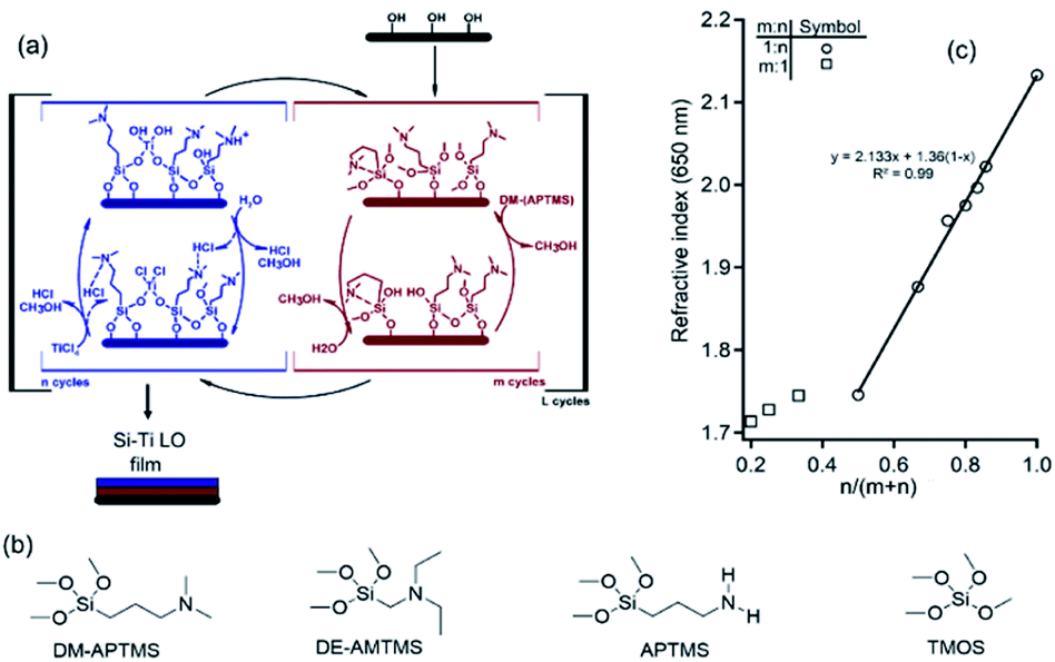 | ||
Fig. 1 (a) CT-M/ALD deposition of Si–Ti LO films depicted with DM-APTMS & H2O (MLD) and TiCl4 & H2O (ALD) precursors, respectively. Where m and n indicate the number of repetitions of the MLD (SiOx) and ALD cycles (TiO2), respectively, and L represent the number of repetitions of the super-cycle. (b) Silane precursors studied, (c) optical properties of Si–Ti LO films. Refractive index of as-deposited films measured at 650 nm for m![[thin space (1/6-em)]](https://www.rsc.org/images/entities/char_2009.gif) :n MLD:ALD super-cycle for increasing TiO2 (○), and SiOx (□) repetitions, respectively, in the super cycle (L = 120). The line presents a linear fit obtained for increasing TiO2 repetitions data, y = 2.133x + 1.36(1 − x) with R2 = 0.99. :n MLD:ALD super-cycle for increasing TiO2 (○), and SiOx (□) repetitions, respectively, in the super cycle (L = 120). The line presents a linear fit obtained for increasing TiO2 repetitions data, y = 2.133x + 1.36(1 − x) with R2 = 0.99. | ||
2. Experimental section
2.1 Tandem M/ALD
Si–Ti LO thin films were prepared using TiCl4 (Acros, 99.9%), N,N-dimethyl-3-aminopropyl trimethoxysilane (DM-APTMS) from Gelest, N,N-diethylaminomethyl trimethoxysilane (DE-AMTMS) from Gelest, (3-aminopropyl)trimethoxysilane (APTMS) from Aldrich, tetramethyl orthosilicate (TMOS) from Sigma-Aldrich and ultra-pure water (>18 MΩ, ELGA purification system). Ultra-high purity Ar gas was used as the carrier gas and purge in a hot wall reactor. The duration of precursor dosing was controlled using computer controlled pneumatic valves with a steady state working pressure of 1.5 × 10⁻¹ mbar maintained during the process.The process consists of two parts:
(i) MLD deposition of SiOx with a Si–C bond, where ‘x’ is indicating a non-stoichiometric oxide phase using alkoxysilane and water termed here MLD cycle, repeated (m) times.
(ii) ALD deposition of TiO2 using TiCl4 and water termed here ALD cycle, repeated (n) times.
Film deposition consisting of the two parts, (i) followed by (ii) is termed a super-cycle, repeated (L) times (Fig. 1a and b). Unless otherwise mentioned, typically L = 120 M/ALD cycles for the Si–Ti LO films used for characterization and analysis. The optimized conditions were determined by attaining saturation in film thickness with complete surface reaction in the exposure step and complete removal of volatile residues in the purge step to avoid side-reactions. DM-APTMS, TMOS and APTMS kept at oven set to 80 °C. DE-AMTMS kept at oven set to 95 °C. The sample temperature was set to 153 °C unless otherwise mentioned. Si–Ti LO films prepared by DM-APTMS, TiCl4 and water were processed under Ar atmosphere at different temperatures for 20 minutes, termed here film calcination.
2.2 In situ quadrupole mass spectroscopy
The volatile fragments released during Si–Ti LO M/ALD process were characterized by in situ quadrupole mass spectroscopy, SRS CIS 300, with electron multiplier detector.2.3 XPS measurements
X-ray photoelectron spectroscopy (XPS) data was collected with a Kratos Axis Ultra X-ray photoelectron spectrometer. Spectra were acquired with monochromatic Al Kα radiation.2.4 Raman measurements
Raman spectra were collected on a Renishaw inVia (Gloucestershire, UK) Raman spectrometer, operated as follows: Ar+ laser (514.5 nm), 50× magnification.2.5 Four-point probe sheet resistance measurement
Sheet resistance was measured using four-point probe setup (Jandel, RM3-AR).2.6 Ellipsometry
Refractive index and optical thickness of the films were measured by spectroscopic ellipsometry. Measurements were performed using variable-angle spectroscopic ellipsometry (VASE) at wavelengths from 300 nm to 900 nm. Cauchy modeling was adopted to extract film thickness and the refractive index at 650 nm considering low energy regime without absorption.2.7 X-ray diffraction
Rigaku SmartLab X-ray diffractometer (Cu Kα radiation (λ = 1.54 Å), 40 kV and 30 mA) was used to evaluate the oxide crystallinity and phases. The diffractometer was operated at a low angle of incidence (α was set to 0.5°), i.e., grazing incidence X-ray diffraction (GIXRD) geometry was used.2.8 Scanning tunneling microscopy and spectroscopy
The tunneling spectra were acquired using a home-built room-temperature STM and a Pt–Ir tip. The STM topographic images were typically measured with sample-bias and current set values of V = 2 V and I = 1 nA, whereas the tunneling I–V curves were acquired with set values (before disabling the feedback loop for spectrum acquisition) of I = 1 nA and at variable voltages to confirm that the apparent gaps do not depend on the setting. Band gaps were determined form the difference between the voltage values at which the tunneling current onset was obtained at positive and negative sample bias voltage.2.9 Conductive atomic force microscopy
The C-AFM data were taken using a commercial (NT-NDT Ntegra) AFM system with metal (TiN and TiPt) coated silicon tips. Here, current maps and topographic images are acquired simultaneously several mm from the Au electrode, both in the contact (constant-force) mode.3. Results and discussion
3.1 Optical properties of as-deposited Si–Ti LO thin films
The refractive index was obtained by spectroscopic ellipsometry for Si–Ti LO films deposited with varying Ti (n repetitions) to Si (m repetitions) in the super cycle repeated (L = 120) (Fig. 1c). The graph presents the measured refractive index vs. number of ALD cycles normalized to the sum of the ALD and MLD cycles in the tandem process, showing a linear correlation for the range 1.75 to 2.13. In this range, where TiO2 repetitions is increased (n), the Si–Ti LO films exhibit tunable refractive index corresponding to the Si-, and Ti-oxide fraction of the film. The measured refractive indices of the nanocomposite films (data presented in Fig. 1c) was accounted for by considering the weighted contribution of the SiOx and TiO2 phases according to the n, m dose in the CT-M/ALD process (eqn (1)):
 | (1) |
3.2 Electrical properties of calcined Si–Ti LO thin films
Tailoring the electronic and optical properties of mixed oxide films often involve varying film composition by post deposition treatment under various conditions.25,26 The catalytic tandem M/ALD process studied here was used to prepare Si–Ti LO films that were thermally treated under Ar atmosphere (calcined) resulting in films exhibiting an insulator to semiconducting characteristics. During heat treatment under Ar atmosphere the resulting Si–Ti LO films gain electrical conductivity with tunable conductivity in a wide range spanning over several orders of magnitude (Fig. 2a). The resistivity of calcined Si–Ti LO films with one MLD cycle (m = 1) and increasing number of ALD cycles (n) decreased up to n ∼ 3 or 4, depending on the post-deposition processing temperature and showed no further significant decrease for higher number of ALD steps in the super-cycle sequence (Fig. 2a). Increasing the number of ALD cycles changes the proportion of the TiO2 phase to the SiOx phase in the film. When the composite films were calcined under Ar atmosphere, sub-stoichiometric metallic-like (TiOx) phases were formed. This observation is in accord with ref. 27 reporting the formation of metal-like (TiOx) thin films, resulting in conductive films by thermal processing in Ar atmosphere films deposited by pulsed laser deposition. The conductivity trends upon thermal processing were further studied for other type of organic–inorganic hybrid films prepared by MLD, such as Ti–EG (titanium–ethylene glycol). This allows to compare the conductivity changes upon thermal treatment for Ti oxide organic hybrid thin films and the Si–Ti LO films where, in addition, a Si–C bond is introduced to promote internal Red–Ox processes between the Si- and Ti-oxide layered oxide components.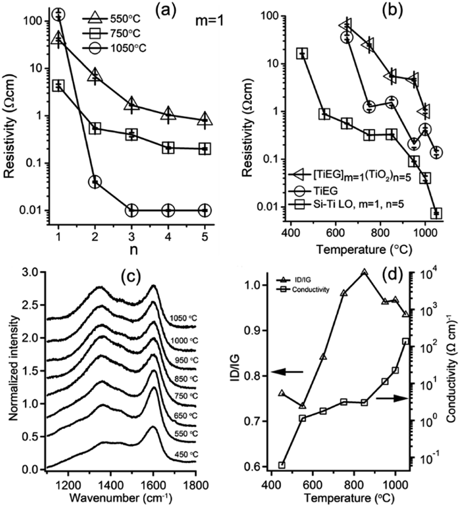 | ||
| Fig. 2 Evolution of various physical properties of Si–Ti LO films calcined under Ar atmosphere. (a) Resistivity of Si–Ti LO films vs. M/ALD super-cycle details (m = 1, n = 1 to 5), (b) comparison of resistivity of Si–Ti LO films, Ti–EG and Ti–EG–TiO2 films calcined under Ar atmosphere, (c) Raman spectra for various treatment temperatures, and (d) intensity ratio of D to G Raman bands and conductivity vs. calcination temperature (m = 1, n = 5). DM-APTMS precursor used to deposit Si–Ti LO films. | ||
The resistivity Si–Ti LO films with m = 1 and n = 5, Ti–EG, Ti–EGm=1(TiO2)n=5, and pure TiO2 films were studied for various processing temperatures in the range of 450–1050 °C under Ar (Fig. 2b). All properties were measured after the samples were processed at the specified temperature and cooled to RT under Ar to avoid additional processes. Ti–EG films were prepared by MLD process of TiCl4 and EG, whereas Ti–EGm=1(TiO2)n=5 films were prepared by MLD-ALD process of TiCl4, EG and H2O. Pure TiO2 films calcined in the range of 450–1050 °C exhibit high resistance, above the contact limit of our measurement setup, and therefore sheet resistance values could not be measured. Ti–EG films calcined in Ar gave the resistivity in the range of 36–0.14 Ω cm showing a decreasing resistivity trend with increased temperature, where resistivity values for Si–Ti LO with m = 1 and n = 5 resulted in the lowest resistivity for all temperatures, and Ti–EGm=1(TiO2)n=5 films showing the highest values (Fig. 2b). The decrease in resistivity between the three types of films spanning over several orders of magnitude for each calcination temperature can be attributed to the evolution of oxygen deficient titanium oxide (TiOx) and to the formation of a graphitic phase by thermal decomposition of the organic part of the film under Ar. This result agrees with the range of resistivity and the conclusion reported by Aziz et al. for pyrolysis of Ti–GL (glycerol) films under Ar atmosphere at similar range of temperatures.28 Combination of Ti–EG and a TiO2 films [Ti–EGm=1(TiO2)n=5] show higher resistivity than Ti–EG films at the whole range of processing temperatures. This result can be accounted by the fully oxidized TiO2 which is an insulator with a reported resistivity in the order of ∼105 to 106 Ω cm at room temperature for the rutile phase.29 Si–Ti LO films prepared with m = 1, n = 5 showed lower resistivity (higher conductivity) for all temperatures studied. In order to obtain further insight regarding the low resistivity of these films, Raman and XPS analysis were applied. Raman spectra of Si–Ti LO films prepared with m = 1, n = 5 revealed characteristic D and G bands at 1350 cm−1 and 1605 cm−1 respectively (Fig. 2c). The intensity ratio between D and G bands usually reflects the graphitic ordering. Analysis of D and G bands in Si–Ti LO films with m = 1, n = 5 following calcination under Ar atmosphere shows D/G band ratio that increases with processing temperature, and above 850 °C the D/G ratio exhibits a slight decrease in contrary to a sharp increase in the conductivity (Fig. 2d). Generally, the electrical conductivity is proportional to the graphitization degree of the material and the G band intensity is a measure of the degree of graphitization. However, for Ar processed Si–Ti LO films the electrical conductivity of the film has a complicated correlation with D/G ratio which is not explained by considering only the graphitic phase since additional conductive phases are involved, as further demonstrated below.
3.3 Electrical properties of calcined Si–Ti LO thin films studied by scanning tunneling spectroscopy (STS)
Spatially resolved tunneling spectra were measured at various locations on each sample and correlated with the macroscopic data obtained by optical absorption spectra of the same thin films (Fig. 3a–d). In particular, the spatial distribution and abundance of band-gaps (BGs) extracted from the STS data are compared with those manifested by the optical spectra showing dual BG structure (Fig. 3e and f). Such comparison is important for two main reasons. First, the tunneling spectra measure the fundamental (single-particle) BG because the conduction and valence bands are monitored separately, while optical absorption spectra measure the excitonic BG that is usually smaller than the fundamental gap due to the electron–hole Coulomb interaction.30,31 Therefore, and quite importantly, this interaction energy can be estimated by comparing the two measured gaps. Second, as mentioned above, the spatially resolved tunneling spectra can shed light on the origin of the dual gaps suggested by the optical absorption data that average over the whole sample. STS measurements on two samples calcined under Ar, (Rs = 335 kΩ sq−1 and 125 kΩ sq−1) exhibited two types of I–V characteristics; one showing a clear gap of ∼2.8 eV and the other a metallic, gapless structure (Fig. 3a and b). The abundance of the gapped areas reduced with increasing film conductivity. Interestingly, the spectra measured on the R = 335 kΩ sq−1 sample suggest that it is n-type doped, as the chemical potential (zero-bias) is shifted towards the conduction-band edge (onset of current at positive sample bias). Data measured on a more resistive sample (R = 4.47 MΩ sq−1), reveal three types I–V characteristics on spatially separated regions. Most of the sample area shows I–V curves with gaps of two sizes, ∼1.8 eV and ∼3.2 eV (Fig. 3c). This is consistent with the optical band gap details revealed by the optical absorption measurements (Fig. 3e and f). However, metallic-like (gapless) regions were also found (Fig. 3d), similar to previous studies on VO2 that indicated the existence of metallic ‘pockets’ in the insulating phase.32,33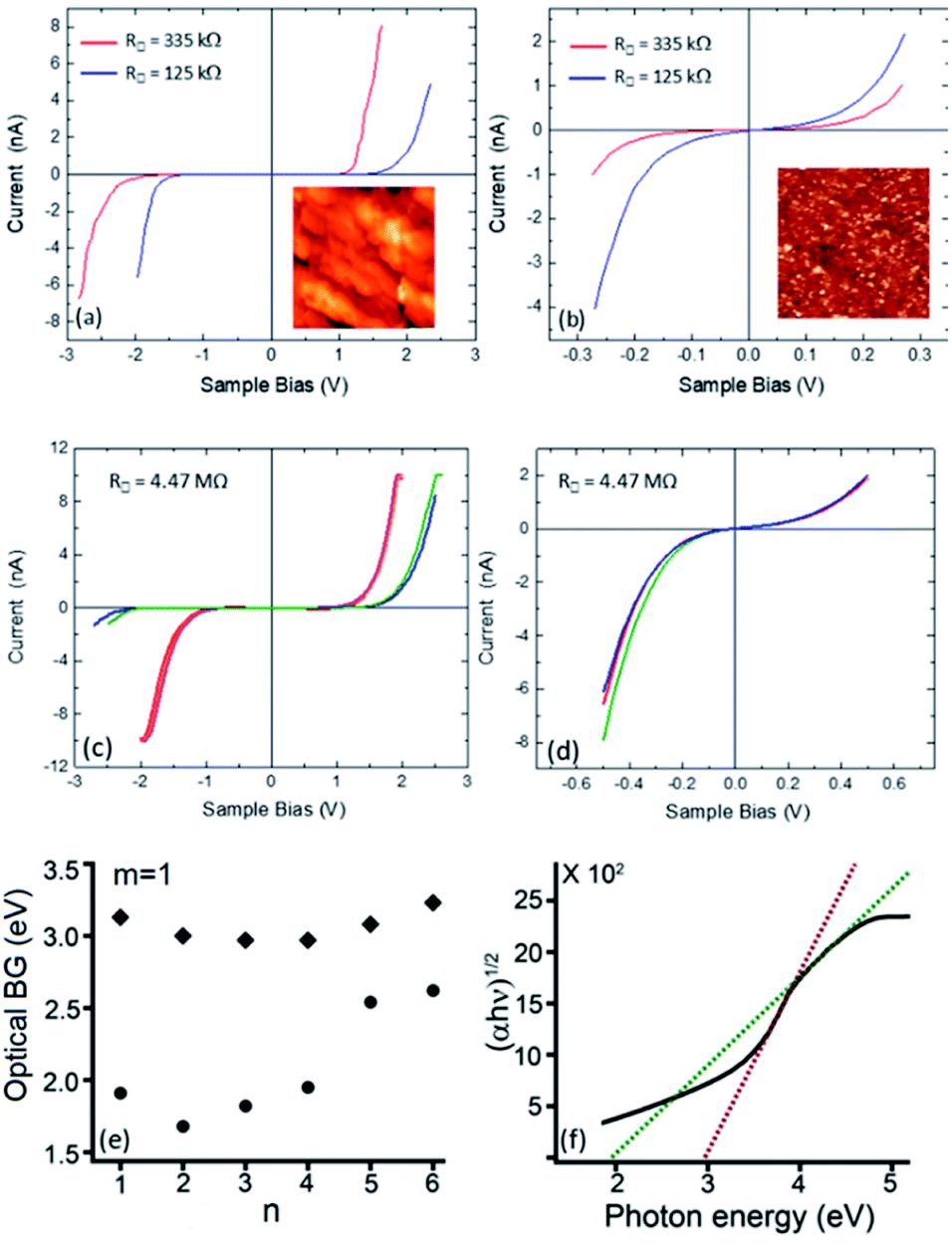 | ||
| Fig. 3 Typical tunneling I–V curves for calcined Si–Ti LO films (m = 1, n = 5, L = 120, DM-APTMS). (a, b) Film calcined at 550 °C, red traces, Rs = 335 kΩ sq−1, and at 750 °C, blue traces, Rs = 125 kΩ sq−1, respectively. Two types of I–V characteristics were found on different regions of the samples, showing gaps of around 2.8 eV (a) and gapless metallic-like behavior (b). Inset of (a) portrays a 300 × 300 nm2 STM topographic image of the sample calcined at 550 °C. Inset of (b) depicts a 2 × 2 μm2 AFM image of the sample calcined at 750 °C. Full color scale in both images is 10 nm. (c, d) Typical tunneling I–V characteristics measured on a sample of sheet resistances, R = 4.47 MΩ. Three types of spectra were found, on spatially separated regions, showing: (c) gaps of sizes ∼3.2 eV (green and blue curves), gaps of sizes ∼1.8 eV (red, orange, magenta curves); and (d) gapless metallic-like behavior. Optical BGs determined for films calcined at 850 °C, (e) optical BG values determined for (m = 1, n = 1 to 6, L = 120, DM-APTMS), and (f) typical Tauc plot analysis presented for (m = 1, n = 4, L = 120, DM-APTMS) from which the BG values were determined. | ||
3.4 Electrical properties of calcined Si–Ti LO thin films by conductive atomic force microscopy (C-AFM)
C-AFM provides information on the local electrical transport properties and thus yields further insight into the spatial distribution of areas of different conductivities within the sample. In C-AFM, the current between a conductive tip and an external electrode deposited on the sample surface is measured along with the topography (Fig. 4), and the obtained current maps resolve the preferred current paths.34,35 Fig. 4a portrays the C-AFM measurement configuration applied here, in which current between a conductive tip and a pre-fabricated Au electrode is measured (as a function of tip bias, VB) along with the topography. Typical results acquired from the R = 335 kΩ film are presented in Fig. 4b (topography) and Fig. 4c (current maps at VB = 2 V). The current maps are further analyzed in Fig. 4d. The C-AFM data are consistent with the STS results, the former showing distribution in the local conductivities while the latter demonstrating a distribution in the BG values and metallic-like regions. It should be noted, however, that the nature of two data sets is fundamentally different and therefore they are complementary to one another. STS is a predominantly surface-sensitive method, yielding information on the local surface density of states and thus the local BGs whereas C-AFM monitors also the sample's interior properties as the current from the tip to the external electrode can flow also there.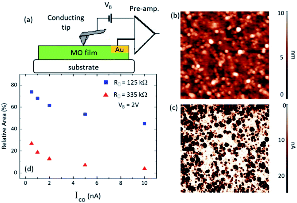 | ||
| Fig. 4 Conductive atomic force microscopy measurements (C-AFM). (a) Scheme of the measurement configuration – current between a conductive AFM tip and an external (Au) electrode is measured along with the topography. (b and c) C-AFM measurement of the Rs = 335 kΩ sq−1 sample with tip bias VB = 2 V. The topographic image is presented in (b) and the corresponding current map in (c). Scan size is 1.5 × 1.5 μm2. (d) Conductive area percentage showing currents larger than a cutoff value Ico. Metal electrodes were evaporated after the thermal processing step. Samples were measured at RT after calcination of the Si–Ti LO films (m = 1, n = 5, L = 120, DM-APTMS). | ||
3.5 Chemical composition and species of calcined Si–Ti LO thin films studied by X-ray photoelectron spectroscopy (XPS)
XPS was applied to study the chemical composition of the Si–Ti LO films after thermal processing under Ar atmosphere. All measurements were performed under vacuum at RT. Deconvolution of O1s and Ti2p peaks to species showed value of ∼2 in the calcination temperature range of 450–1000 °C, as expected for the TiO2 phase (Fig. 5a–c). In contrast, increasing atomic ratio of O1s{Si–
![[O with combining low line]](https://www.rsc.org/images/entities/b_char_004f_0332.gif) –Ti}/Ti2p species imply the evolution of an additional oxide phase (Fig. 5c). Analysis of the conductivity of Si–Ti LO films with m = 1, n = 5 vs. the atomic% ratio of O1s{Si–
–Ti}/Ti2p species imply the evolution of an additional oxide phase (Fig. 5c). Analysis of the conductivity of Si–Ti LO films with m = 1, n = 5 vs. the atomic% ratio of O1s{Si–![[O with combining low line]](https://www.rsc.org/images/entities/char_004f_0332.gif) –Ti}/Ti2p reveals two regimes associated with the calcination process and the stoichiometry of the film. Below 850 °C the conductivity increases slightly with temperature and from 850 °C and above the sharp increase in conductivity corresponding to stoichiometry ratios of ∼1.5–1.6 for O1s/Ti2p indicate that the conductivity mostly affected by the formation of sub-stoichiometric TiOx (1.5 < x < 1.6). Formation of oxygen deficient TiOx from TiO2 can be explained by loss of oxygen to the Si phase by internal redox reaction as further discussed below by considering the Si2p XPS data. Lakshmi Nagarajan et al. reported oxygen deficient gallium oxide, GaOx, with insulator–metal transition upon heating associating the conductivity jump observed to internal redox disproportionation reaction.36 The internal redox reaction between the Si and Ti explored by XPS characterization of Si–Ti films with m = 1, n = 5 on sapphire (Al2O3) substrate to avoid background signals from the sample substrate. Deconvolution of Si peak reveal Si in oxidation states of Si3+ at BE of 102.5 ± 0.2 eV and Si4+ at 103.4 ± 0.2 eV (Fig. 5e). XPS analysis of the relative contribution of the Si species reveal that up to 850 °C most of the film consist Si3+ (Si2O3) (Fig. 5f). However, above 850 °C Si4+ (SiO2) species contribution increased markedly and Si3+ species contribution decreased dramatically with most of the film consisting of SiO2 following calcination at 1050 °C. The oxidation state of silicon in films after calcination at high temperatures under Ar suggest that SiOx phase, which has a labile Si–C bond, where the alkylamine functionality links, functioning as a reducing agent while TiO2 act an oxidant resulting in formation of sub-stoichiometric TiOx phases. Hence, the higher conductivity of the Si–Ti LO films following calcination above 850 °C was due to the formation of sub-stoichiometric oxides of titanium, also commonly referred to as Magnéli phases and have the formula TinO2n−1 where n is an integer of 4 or more. Examples of sub-stoichiometric oxides of titanium include Ti4O7, Ti5O9, Ti6O11.23 Upon thermal processing under inert atmosphere, the following internal rearrangement takes place: [SiOx]; [TiO2] → [SiO2]; [TinO(2n−1)] and formation of an additional graphitic phase resulting from the decomposition of the alkyl substituent. Further crystallographic and Raman analyses presented below support this conclusion.
–Ti}/Ti2p reveals two regimes associated with the calcination process and the stoichiometry of the film. Below 850 °C the conductivity increases slightly with temperature and from 850 °C and above the sharp increase in conductivity corresponding to stoichiometry ratios of ∼1.5–1.6 for O1s/Ti2p indicate that the conductivity mostly affected by the formation of sub-stoichiometric TiOx (1.5 < x < 1.6). Formation of oxygen deficient TiOx from TiO2 can be explained by loss of oxygen to the Si phase by internal redox reaction as further discussed below by considering the Si2p XPS data. Lakshmi Nagarajan et al. reported oxygen deficient gallium oxide, GaOx, with insulator–metal transition upon heating associating the conductivity jump observed to internal redox disproportionation reaction.36 The internal redox reaction between the Si and Ti explored by XPS characterization of Si–Ti films with m = 1, n = 5 on sapphire (Al2O3) substrate to avoid background signals from the sample substrate. Deconvolution of Si peak reveal Si in oxidation states of Si3+ at BE of 102.5 ± 0.2 eV and Si4+ at 103.4 ± 0.2 eV (Fig. 5e). XPS analysis of the relative contribution of the Si species reveal that up to 850 °C most of the film consist Si3+ (Si2O3) (Fig. 5f). However, above 850 °C Si4+ (SiO2) species contribution increased markedly and Si3+ species contribution decreased dramatically with most of the film consisting of SiO2 following calcination at 1050 °C. The oxidation state of silicon in films after calcination at high temperatures under Ar suggest that SiOx phase, which has a labile Si–C bond, where the alkylamine functionality links, functioning as a reducing agent while TiO2 act an oxidant resulting in formation of sub-stoichiometric TiOx phases. Hence, the higher conductivity of the Si–Ti LO films following calcination above 850 °C was due to the formation of sub-stoichiometric oxides of titanium, also commonly referred to as Magnéli phases and have the formula TinO2n−1 where n is an integer of 4 or more. Examples of sub-stoichiometric oxides of titanium include Ti4O7, Ti5O9, Ti6O11.23 Upon thermal processing under inert atmosphere, the following internal rearrangement takes place: [SiOx]; [TiO2] → [SiO2]; [TinO(2n−1)] and formation of an additional graphitic phase resulting from the decomposition of the alkyl substituent. Further crystallographic and Raman analyses presented below support this conclusion.
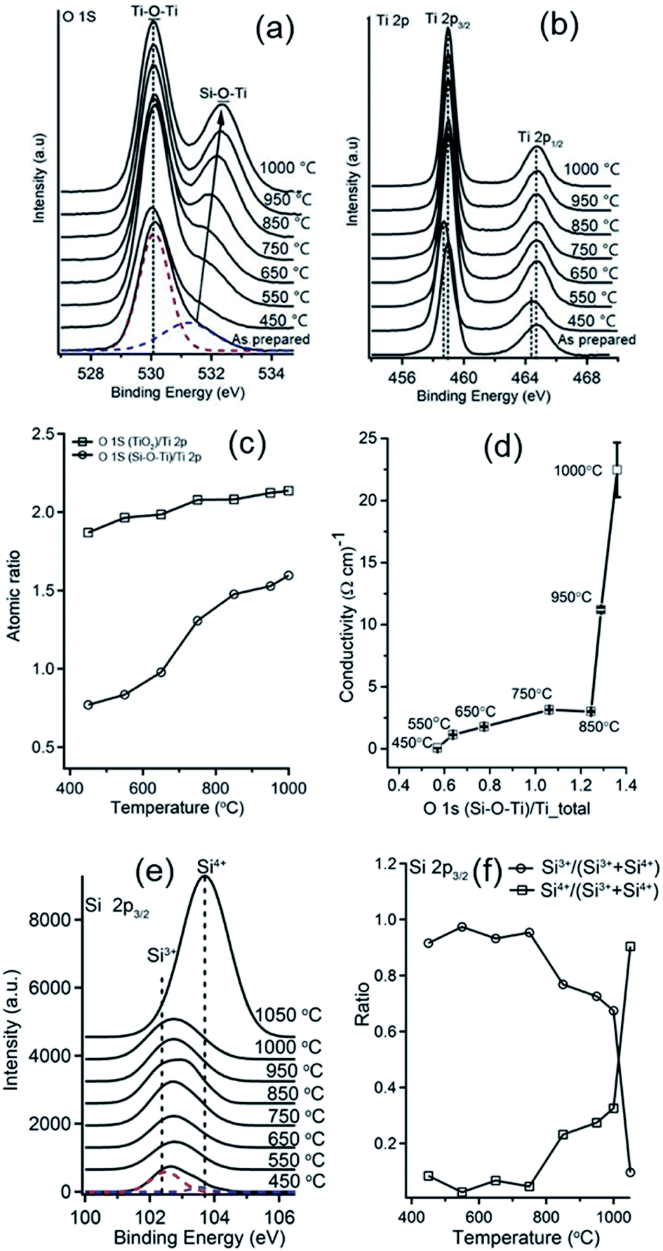 | ||
| Fig. 5 XPS analysis for Si–Ti LO films after calcination at specified temperatures under Ar measured under vacuum at RT. (a) O1s XPS spectra (b) Ti2p XPS spectra (c) O1s{Ti2}/Ti2p atomic ratios of indicated species vs. temperatures. (d) Film conductivity vs. O1s{Si––Ti}/Ti2p ratios. (e) Si2p XPS spectra (f) relative contribution of Si3+ and Si4+ species. Si–Ti LO films (m = 1, n = 5, L = 120, DM-APTMS). | ||
3.6 Crystal phases of calcined Si–Ti LO films
X-ray analysis showed TiO2 anatase phase (ICDD PDF#01-070-6826) for Si–Ti LO films with m = 1, n = 5 calcined below 1050 °C under Ar atmosphere. All films exhibited polycrystalline nature with slightly different degrees of orientation with increasing temperature. Films processed at 1050 °C, displayed Magnéli phases (TinO2n−1, 4 < n < 10), the diffraction peak positions were consistent with Ti4O7 (ICC PDF#00-050-078) and Ti6O11 (ICDD PDF#00-050-0788). Because of the wide line broadening (most probably due to small crystallite size) and peak superposition it is rather difficult to identify the specific Magnéli phase based on XRD pattern alone. Both XPS and Raman analysis suggest the formation of Magnéli phase at lower temperatures, below 850 °C (Fig. 5c and 6b), however those are not detectable by XRD until large enough crystallite formed at 1050 °C. To elucidate the Magnéli phase for Si–Ti LO thin films calcined at lower temperatures, where the application of X-ray diffraction may be limited, the films were studied using Raman analysis in the wavenumber region ranging from 100 cm−1 to 900 cm−1. TiO2 anatase show six active Raman modes (A1g + 2B1g + 3Eg) and three infrared (IR) active modes (A2u + 2Eu).24 In rutile TiO2 four vibration modes (A1g + B1g + B1g + Eg) are Raman active and four vibration modes are IR active (A2u + 3E).26 In Fig. 6b, the peak at 146 cm−1 corresponds to anatase Eg and the peak at 610 cm−1 corresponds to rutile A1g mode. The Eg mode is associated with planar O–O interactions while A1g and B1g modes originate from Ti–O stretching modes.37 A broad peak appeared approximately at 260 cm−1 (Eg) revealing a defect induced disorder due to oxygen deficiency.38 All films shows a peak at 260 cm−1, it corresponding to the reported band for Magnéli phase.39 A strong peak at 420 cm−1 for all post-deposition processing temperatures was attributed to the Ti6O11 Magnéli phase.40 The sub-stoichiometric Magnéli phases of titania show higher electronic conductivity.41 We suggest that the formation of conductive phases in relatively low temperature owing to the layer structure of the films obtained by the M/ALD process where Si act as a reducing agent and catalyzed stoichiometric titanium dioxide to Magnéli phase formation by internal redox reaction. The film conductivity increases sharply for temperatures 850 °C and higher, suggesting that both the formation of Ti6O11 Magnéli and graphitic phases are important for the overall conductivity of the films.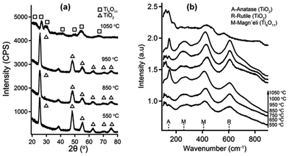 | ||
| Fig. 6 (a) X-ray diffraction (GIXRD) and (b) Raman spectra for Si–Ti LO films calcined under Ar at the specified temperatures. Samples were measured at RT after calcination of the Si–Ti LO films (m = 1, n = 5, L = 120, DM-APTMS). | ||
3.7 Deposition characteristics of Si–Ti LO films for 1![[thin space (1/6-em)]](https://www.rsc.org/images/entities/h3_char_2009.gif) :1 MLD:ALD super cycles
:1 MLD:ALD super cycles
The M/ALD process was optimized for four types of silane precursors, DM-APTMS, DE-AMTMS, APTMS, and TMOS (optimized process parameters are provided in the ESI, Table S1†). These amine silane precursors were selected for elucidating mechanistic details of the CT-M/ALD process. DM-APTMS and DE-AMTMS contains propyl and methyl linkers between the amine and –Si functionalities, respectively, allowing to compare inter vs. intra-molecular amine assisted catalysis. DM-APTMS and APTMS contains tertiary vs. primary amine functionality, and TMOS contains no amine functionality. Ellipsometry measurements of the optimized M/ALD processes showed linear film growth with M/ALD cycles (L) for all silane precursors studied for both MLD and ALD processes (Fig. 7a). Growth per cycle (GPC) values for the tandem M/ALD processes were 2.40 Å per cycle for DE-AMTMS, 1.90 Å per cycle for DM-APTMS, and 1.80 Å per cycle for APTMS compared to TMOS with 0.75 Å per cycle, showing a substantially lower value (Fig. 7a and b). In ALD and MLD processes, GPC values are determined by multiple factors including completeness of surface reactions, molecular orientation at the surface, packing, tilt, double surface reactions, etch and desorption, and steric hindrance by bulky organic precursors.42 The GPC values obtained for the precursors studied here point at the role of the embedded amine functionality present in the first three precursors, acting as a Lewis base catalyst in the film deposition process in contrast to TMOS, where no amine functionality is present and a much lower GPC value was obtained. Additionally, the GPC values follows the amine basicity trend with higher basicity of the dimethyl amine in DM-APTMS resulted in higher GPC value compared with APTMS. The amine functionality forming possibly both intra- and inter-molecular Lewis acid–base interactions that catalyze the alkoxysilane condensation and hydrolysis reactions and overall, the film growth. Under acidic conditions, such as present in the in situ formation of HCl by hydrolysis of TiCl4, acid–base catalytic reactions take place as well. For the DE-AMTMS precursor the amine is linked to silicon through a methylene bridge which allows the catalysis to occur only through inter-molecular interactions since intramolecular coordination of N: to Si is not accessible. Additionally, the short linkage of the base functionality in DE-AMTMS decreases the probability of steric hindrance, tilted molecular orientation, and self-coordination towards Si, making this moiety more efficient for retaining protons at the surface, and possibly yielding the higher GPC value.
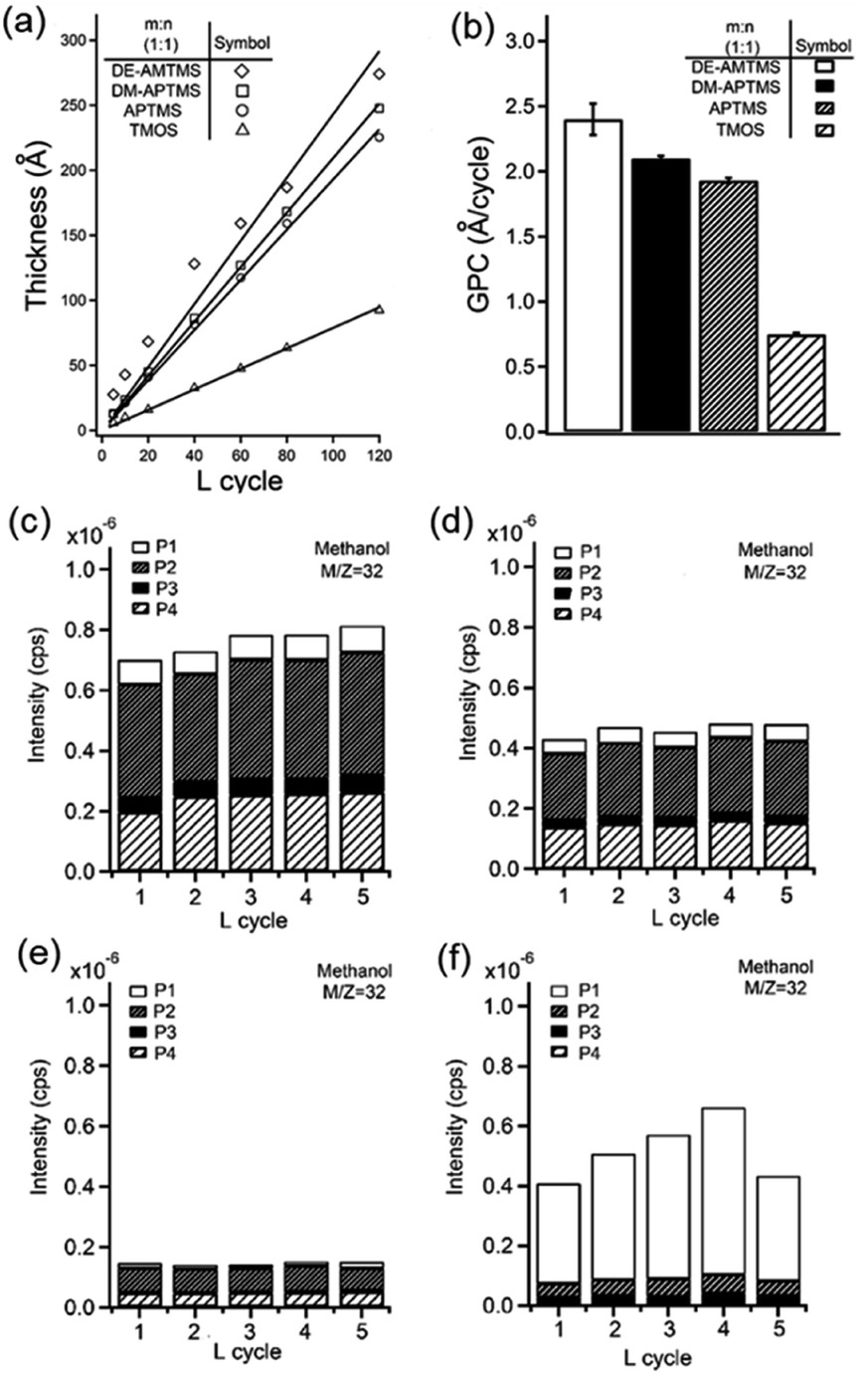 | ||
| Fig. 7 Si–Ti LO M/ALD process. (a) Thickness vs. cycles (marker size represent experimental error limit) {y = 2.4x, R2 = 0.95 for DE-AMTMS, y = 2.1x, R2 = 0.99 for DM-APTMS, y = 1.9x, R2 = 0.99 for APTMS, y = 0.9x, R2 = 0.99 for TMOS} and (b) growth per cycle (GPC) comparison for DE-AMTMS, DM-APTMS, APTMS and TMOS for 1:1 MLD:ALD process. (c–f) In situ quadrupole mass spectroscopy (MS) for M/ALD film deposition. Methanol signal (m/z = 32) shown for silane step (P1), H2O after silane step (P2), TiCl4 step (P3) and H2O after TiCl4 step (P4) for (c) DM-APTMS, (d) APTMS, (e) TMOS and (f) DE-AMTMS. Processes performed at 85 °C (stack-bar graph presentation). | ||
Catalytic ALD was previously reported for lowering in the deposition temperature of SiO2 by ALD by the addition of ammonia vapor as Lewis base catalyst.43 Furthermore, self-catalytic ALD of SiO2 using an embedded amine functionality was reported by Julien Bachmann et al., where (3-aminopropyl)trimethoxysilane was used for film growth.16 It was demonstrated that the Lewis base function as catalyst in the process, however the report could not determine if the main mode of catalysis is of inter- or intra-molecular nature. Our results suggest that the inter-molecular path is dominant for DE-AMTMS. Furthermore, MLD alone, without ALD process of TiCl4 and water under the same conditions resulted in a thin layer with approximately constant thickness of 14 Å, 13 Å and 3.5 Å for DM-APTMS, APTMS, and DE-AMTMS respectively, regardless of the number of MLD cycles applied. The constant thickness and lack of linear film growth with number of cycles for MLD-only process suggest that the reactivity of DM-APTMS/APTMS/DE-AMTMS and H2O alone is not sufficient for film growth under these conditions and that the acidic HCl evolved in the ALD step catalyze the synthesis, establishing the acid–base catalysis mechanism. This result is in agreement with the solution phase the hydrolysis and condensation of silanes which does not go to completion even with addition of an acidic catalyst.44 Similarly, it is reasonable to assume that for the vapor phase process some fraction of the methoxy groups of the alkoxy silane precursor is hydrolyzed leaving some non-hydrolyzed groups when exposed to the water vapor. Such partial hydrolysis reactions result in lower GPC values since the silane precursor having non-hydrolyzed methoxy groups result in non-active surface sites that cannot contribute to the overall growth of the film.
The CT-M/ALD process was further characterized by in situ quadrupole mass spectroscopy (MS) by monitoring the methanol fragment (m/z = 32) signal during the CT-M/ALD processes indicative of the hydrolysis of the methoxy-Si functionality used as the siloxane precursors. In situ MS data was collected for multiple consecutive repetitions of the CT-M/ALD cycles showing consistent profile for each (Fig. 7c–f). For DM-APTMS, APTMS and TMOS low levels of methanol obtained in the first exposure step, P1, (silane exposure) (Fig. 7c–e) attributed to residual hydrolysis of the methoxy groups by hydroxylated species at the surface. In the following step, P2, the exposure of H2O resulted in increased methanol level indicating further hydrolysis during the film growth in this step. Traces of methanol were observed following the TiCl4 exposure, P3, suggesting that the protons (HCl) released from the hydrolysis of Ti–Cl contribute to the catalytic hydrolysis and condensation reactions as expected for acid catalysis. In the last step, P4, the exposure of H2O significant methanol signal is obtained which referred to the hydrolysis of the silane methoxy groups following the adsorption of protons resulting in the overall acid–base catalysis. In all deposition steps the increasing in methanol signal trend followed TMOS, APTMS and DM-APTMS suggesting that the amine functionality assist in film growth by acting both as a Lewis base in the MLD step and as a proton sponge in the ALD step. In contrast, M/ALD supercycle with DE-AMTMS resulted with a different fingerprint of the methanol signal for P1–P4 process steps. The highest methanol levels were measured at P1 with significantly lower levels for P2–P4. Hence, most of the hydrolysis occurs at the MLD step when at P1 most of the methoxy groups hydrolyzed. This result suggests a different reaction profile for M/ALD using DE-AMTMS compared to the other amine alkoxysilane precursors where the amine is linked with a longer molecular chain pointing at the roles of inter- vs. intra-Lewis-base catalysis promoted by the amine functionality.
3.8 Deposition characteristics of Si–Ti LO films for m:n M/ALD super cycles
Films were deposited for various super-cycle sequences by varying the number of MLD cycles (m) and ALD cycles (n) during the growth of the film. Linear increase in film thickness deposition was obtained for various ratios of MLD:ALD (m:n) using DM-APTMS, TiCl4 and water in the range of 4:1 to 1:5 for m:n, respectively (Fig. 8a). The catalytic tandem M/ALD process can be used to control the nanocomposite films composition and properties as demonstrated by further characterization by XPS surface analysis. Analysis of the incremental GPC change with number of ALD cycles (n) and number of MLD cycles (m), gave linear trends for all super-cycle processes (Fig. 8b). The linear increment reflects the relative growth of each of the oxide phases, TiO2, and SiOx, corresponding to the ALD and MLD cycle repetition within the process super-cycle. GPC increment (GPC difference obtained for the process when increasing n to n + 1) for TiO2 of 0.65 Å per cycle is in good agreement with previously reported values of 0.40 to 0.70 Å per cycle at substrate temperatures of 150–400 °C for purely TiO2 ALD results obtained under similar conditions. The GPC increment obtained for SiOx (GPC difference obtained for the process when increasing m to m + 1) of 0.48 Å per cycles slightly lower than the pure SiO2 GPC reported values (0.6–0.8 Å per cycle).16,44,45
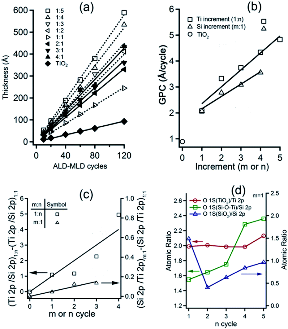 | ||
| Fig. 8 Si–Ti LO CT-M/ALD for m:n processes. (a) Thickness vs. cycles and (b) growth per cycle (GPC) vs. m cycles of MLD, n cycles of ALD for M/ALD processes in the range of 4:1 to 1:5 (m:n) and for m = 0 (only ALD of TiO2). Marker size represent error limit {y = 0.65x + 1.70, R2 = 0.95 for Ti increment; y = 0.48x + 1.69, R2 = 0.97 for Si increment}. (c) Atomic ratios of Ti and Si species for Si–Ti LO films obtained by XPS analysis {y = x, R2 = 0.85 for 1; n; y = 0.05x, R2 = 0.93 for m:1}. (d) Atomic ratios obtained by XPS for the specified species for Si–Ti LO films for varying ALD cycles (n) and constant MLD cycle (m = 1). | ||
X-ray photoelectron spectroscopy (XPS) was used to quantify the atomic composition of the films as a function of various MLD:ALD (m:n) process parameters (Table S2†). N1s XPS spectra showed two peaks centered at 399.9 and 401.9–402.5 eV corresponding to non-protonated (free base) and protonated amine functionality, with stoichiometric ratio of ∼3:7. This result further supports the role of the embedded amine functionality in retaining the acidic protons evolving as side-products in the ALD step (Table S2 and Fig. S3i, j†). C1s XPS spectra showed several peaks with BE corresponding to chemical species of ![[C with combining low line]](https://www.rsc.org/images/entities/char_0043_0332.gif) –O around 286.3 eV and –H around 285.0 eV which correspond to the carbon present in the methoxy and the propyl functionalities of DM-APTMS precursor, respectively. Additional small peak at 288.4–288.8 eV corresponding to O–
–O around 286.3 eV and –H around 285.0 eV which correspond to the carbon present in the methoxy and the propyl functionalities of DM-APTMS precursor, respectively. Additional small peak at 288.4–288.8 eV corresponding to O–![[double bond, length as m-dash]](https://www.rsc.org/images/entities/char_e001.gif) O was also observed, possibly due to extrinsic carbon contamination in the XPS chamber. O1s XPS spectra showed three peaks centered at 530.0 and 531.2–531.5 and 532.2 eV corresponding to Ti2, Si––Ti and Si2 species, respectively. The Si–O–Ti species at the two phases interface act as ‘cross-linking’ bridges between TiO2 and the SiO2 phases (Fig. S3†). This assignment is in agreement with G. M. Ingo et al., for SiO2–TiO2 systems obtained by sol–gel using TEOS and Ti(OPr′).46 Ti2p3/2 XPS spectra showed two peaks at 457.4 and 459.0 eV corresponding to
O was also observed, possibly due to extrinsic carbon contamination in the XPS chamber. O1s XPS spectra showed three peaks centered at 530.0 and 531.2–531.5 and 532.2 eV corresponding to Ti2, Si––Ti and Si2 species, respectively. The Si–O–Ti species at the two phases interface act as ‘cross-linking’ bridges between TiO2 and the SiO2 phases (Fig. S3†). This assignment is in agreement with G. M. Ingo et al., for SiO2–TiO2 systems obtained by sol–gel using TEOS and Ti(OPr′).46 Ti2p3/2 XPS spectra showed two peaks at 457.4 and 459.0 eV corresponding to ![[T with combining low line]](https://www.rsc.org/images/entities/char_0054_0332.gif) iOx and iO2 species, respectively with the Ti3+ and Ti4+ oxidation states with the former found as a minor component. This assignment of the Ti2p3/2 spectra is in good agreement with Thomas Leichtweiss et al. who studied amorphous and highly non-stoichiometric titania (TiOx) thin films.27 Si2p XPS spectra for all M/ALD ratios were symmetric centered around 102.7 eV (Fig. S3g and h†). This BE is between the typical literature value for SiO2 (103.1 eV) and that of
iOx and iO2 species, respectively with the Ti3+ and Ti4+ oxidation states with the former found as a minor component. This assignment of the Ti2p3/2 spectra is in good agreement with Thomas Leichtweiss et al. who studied amorphous and highly non-stoichiometric titania (TiOx) thin films.27 Si2p XPS spectra for all M/ALD ratios were symmetric centered around 102.7 eV (Fig. S3g and h†). This BE is between the typical literature value for SiO2 (103.1 eV) and that of  (101.8 eV) values corresponding to
  species47 and similar to the BE of poly dimethylsiloxane (PDMS) reported by M. R. Alexander et al.48 Incrementing the ALD cycle (n) component within the M/ALD super-cycle gave linear increase in Ti/Si atomic ratios (Fig. 8c). In contrast, only slight growth of the SiOx film is obtained for incrementing MLD cycles (m), with minor Si/Ti increment of only 5% based on atomic ratios determined by XPS. This result may reflect the lack of available protons released at the ALD step, required for promoting the acid catalysis for the complete hydrolysis of the silane and for attaining high yield film deposition. Varying the composition of Si–Ti LO films by incrementing the ALD cycles (n) resulted in a consistent stoichiometric ratio of 2:1 for O1s(TiO2)/Ti2p(TiO2). Increasing ALD cycles, n, resulted in an increase in O1s(Si––Ti)/Si2p(Si(O)3R) ratio from ∼1.6 for n = 1 to ∼2.4 for n = 5 (Fig. 8d). These results suggest that increasing the ALD repeats within the super-cycle sequence afford effective deposition of TiO2 layer and an increase in Si–O–Ti bonds at the interface of the TiO2 and SiOx phases. This trend may be related to the increase in protonation owing to the amine functionality which promote the hydrolysis of the silane precursor. In addition, films with 1:1 MLD:ALD resulted in stoichiometric ratio of ∼3:2 for O1s(SiO2)/Si2p(Si(O)3R). Incrementing the ALD cycles (n) in this case resulted in a sharp decrease to ∼0.5 for 2 ALD cycles following a monotonic increase of O1s(SiO2)/Si2p(Si(O)3R) stoichiometry to ∼1 for 5 ALD cycles. The initial decrease of O1s(SiO2)/Si2p(Si(O)3R) stoichiometry suggest the possibility of siloxane bond cleavage when exposed to the HCl vapor evolving in the ALD step. The moderate, yet monotonic increase in the ratio that follows may be related to hydroxylation, and possibly full hydrolysis of siloxane and Si–OMe species in the acidic vapor environment obtained by the repeating ALD sequence, and evolving HCl. In addition, the thicker TiO2 layer may act as a passivation layer stabilizing the film from etching yet promote formation of siloxane bonds by acid catalysis. To further study this aspects, tandem M/ALD process was studied by omitting H2O exposure steps and analyzing the GPC trends obtained (see details in ESI, Fig. S1 and S2†).
4. Conclusions
The synthesis of layer-by-layer Si–Ti LO thin films using catalytic tandem M/ALD methodology was introduced. The layered oxide films are transformed by post-deposition thermal processing to the respective nanocomposite oxides while fine tuning the electronic structure and phase composition. As-deposited Si–Ti LO films show tunable optical properties with refractive indices in the range of 1.75 to 2.13 at 650 nm. The refractive index correlated linearly with the contribution of the low- and high-refractive index, SiOx and TiO2 phases, respectively, in the nanocomposite oxide film. Thermal treatment of Si–Ti LO films resulted in conductive films spanning over several orders of magnitude showing higher conductivity compared with calcined TiO2, Ti–EG and TiEGm=1(TiO2)n=5 films for all calcination temperatures studied. Raman analysis showed the presence of D and G bands which indicate disordered carbon (D) and graphite (G) phases incorporated in the films. In addition, the low wave-number Raman spectra region exhibited the presence of conductive Magnéli phase Ti6O11 for all calcined Si–Ti LO films. The optical and electronic properties of Si–Ti LO films and films following thermal processing at a range of temperatures were studied applying both macroscopic (whole-sample) absorption spectra, four-point SR, and local-probe (STS, C-AFM) techniques, revealing co-existence of various phases, including gap-less metallic-like regions and regions with band-gaps of 1.8 and 3.2 eV. XPS analyses support our findings showing sub-stoichiometric TiOx that evolved with post-deposition processing temperature and exhibit Si–O–Ti species. X-ray diffractograms demonstrated the presence of a Magnéli phase Ti6O11 for high calcination temperatures, as well as the typical peaks for anatase and rutile TiO2 phases. We suggest that the higher conductivities obtained at relatively low temperatures, such as at 550 °C, is due to the layer structure in M/ALD Si–Ti LO films that facilitate the Magnéli phase formation by local Red–Ox reactions taking place between the SiOx–TiO2 phases. Collectively, this work presents catalytic tandem M/ALD process for the formation of hybrid organic inorganic Si–Ti LO film with optical and electrical properties tuned by composition and Si–Ti oxide layer interface engineering. This work demonstrates the concept of embedding a meta-stable organic motif by MLD step to facilitate transformation of an oxide phase by taking advantage of precise layer-by-layer deposition of alternating phases enabled by M/ALD.Conflicts of interest
The authors declare that they have no conflict of interest.Acknowledgements
The research was partially supported by the Israel Science Foundation (grant no. 661/16). O. M. thanks support from the Harry de Jur Chair in Applied Science.References
- J. Maçaira, L. Andrade and A. Mendes, Sol. Energy, 2017, 158, 905–916 CrossRef.
- H. Guo, X. Zhang, H. Chen, P. Zhang, H. Liu, H. Chang, W. Zhao, Q. Liao and Y. Cui, Opt. Express, 2013, 21, 21456 CrossRef PubMed.
- X. Sun, K. Hu, J. Tu and K. Chen, Surf. Interfaces, 2021, 24, 101135 CrossRef CAS.
- K. Guan, Surf. Coat. Technol., 2005, 191, 155–160 CrossRef CAS.
- M. M. Rahman, A. J. S. Ahammad, J. H. Jin, S. J. Ahn and J. J. Lee, Sensors, 2010, 10, 4855–4886 CrossRef CAS PubMed.
- F. Yang, J. Zhu, X. Zou, X. Pang, R. Yang, S. Chen, Y. Fang, T. Shao, X. Luo and L. Zhang, Ceram. Int., 2018, 44, 1078–1085 CrossRef CAS.
- S. M. Lee, S. M. Hwang, S. Y. Hwang, T. W. Kim, S. H. Lee, G. C. Park, J. Y. Choi, J. J. Yoon, T. J. Kim, Y. D. Kim, H. Kim, J. H. Lim and J. Joo, Mater. Chem. Phys., 2014, 145, 168–175 CrossRef CAS.
- J.-S. Chen, S. Chao, J.-S. Kao, H. Niu and C.-H. Chen, Appl. Opt., 1996, 35, 90 CrossRef CAS PubMed.
- L. Liljeholm, T. Nyberg, T. Kubart, A. Roos and S. Berg, Vacuum, 2010, 85, 317–321 CrossRef CAS.
- A. Guglya and E. Lyubchenko, Thin films, Elsevier Inc., 2018 Search PubMed.
- A. Hodroj, H. Roussel, A. Crisci, F. Robaut, U. Gottlieb and J. L. Deschanvres, Appl. Surf. Sci., 2006, 253, 363–366 CrossRef CAS.
- S. Larouche, H. Szymanowski, J. E. Klemberg-Sapieha, L. Martinu and S. C. Gujrathi, J. Vac. Sci. Technol., A, 2004, 22, 1200–1207 CrossRef CAS.
- S. M. Rossnagel, A. Sherman and F. Turner, J. Vac. Sci. Technol., B: Microelectron. Nanometer Struct.--Process., Meas., Phenom., 2000, 18, 2016 CrossRef CAS.
- J. W. Klaus and S. M. George, Surf. Sci., 2000, 447, 81–90 CrossRef CAS.
- J. W. Klaus, O. Sneh and S. M. George, Science, 1997, 278, 1934–1936 CrossRef CAS PubMed.
- J. Bachmann, R. Zierold, Y. T. Chong, R. Hauert, C. Sturm, R. Schmidt-Grund, B. Rheinländer, M. Grundmann, U. Gösele and K. Nielsch, Angew. Chem., Int. Ed., 2008, 47, 6177–6179 CrossRef CAS PubMed.
- Y. Zhao and X. Sun, ACS Energy Lett., 2018, 3, 899–914 CrossRef CAS.
- S. Ishchuk, D. H. Taffa, O. Hazut, N. Kaynan and R. Yerushalmi, ACS Nano, 2012, 6, 7263–7269 CrossRef CAS PubMed.
- D. Sarkar, D. H. Taffa, S. Ishchuk, O. Hazut, H. Cohen, G. Toker, M. Asscher and R. Yerushalmi, Chem. Commun., 2014, 50, 9176–9178 RSC.
- D. Sarkar, S. Ishchuk, D. H. Taffa, N. Kaynan, B. A. Berke, T. Bendikov and R. Yerushalmi, J. Phys. Chem. C, 2016, 120, 3853–3862 CrossRef CAS.
- N. Kaynan, B. A. Berke, O. Hazut and R. Yerushalmi, J. Mater. Chem. A, 2014, 2, 13822–13826 RSC.
- S. Jayanthi, D. Sarkar, D. H. Taffa and R. Yerushalmi, Top. Catal., 2021, 64, 297–312 CrossRef CAS.
- L. A. Bursill and B. G. Hyde, Prog. Solid State Chem., 1972, 7, 177–253 CrossRef CAS.
- W. Shimizu, S. Nakamura, T. Sato and Y. Murakami, Langmuir, 2012, 28, 12245–12255 CrossRef CAS PubMed.
- J. Martín-Sánchez, R. Trotta, A. Mariscal, R. Serna, G. Piredda, S. Stroj, J. Edlinger, C. Schimpf, J. Aberl, T. Lettner, J. Wildmann, H. Huang, X. Yuan, D. Ziss, J. Stangl and A. Rastelli, Semicond. Sci. Technol., 2018, 33, 013001 CrossRef.
- I. Yadav, S. Dutta, A. Pandey, N. Yadav, A. Goyal and R. Chatterjee, Ceram. Int., 2020, 46, 19935–19941 CrossRef CAS.
- T. Leichtweiss, R. A. Henning, J. Koettgen, R. M. Schmidt, B. Holländer, M. Martin, M. Wuttig and J. Janek, J. Mater. Chem. A, 2014, 2, 6631–6640 RSC.
- A. I. Abdulagatov, K. E. Terauds, J. J. Travis, A. S. Cavanagh, R. Raj and S. M. George, J. Phys. Chem. C, 2013, 117, 17442–17450 CrossRef CAS.
- M. N. Solovan, P. D. Maryanchuk, V. V. Brus and O. A. Parfenyuk, Inorg. Mater., 2012, 48, 1026–1032 CrossRef CAS.
- U. Banin and O. Millo, Annu. Rev. Phys. Chem., 2003, 54, 465–492 CrossRef CAS PubMed.
- O. Millo, U. Banin, Y. W. Cao and D. Katz, Nature, 1999, 400, 542–544 CrossRef.
- Y. J. Chang, C. H. Koo, J. S. Yang, Y. S. Kim, D. H. Kim, J. S. Lee, T. W. Noh, H. T. Kim and B. G. Chae, Thin Solid Films, 2005, 486, 46–49 CrossRef CAS.
- J. G. Ramírez, A. Sharoni, Y. Dubi, M. E. Gómez and I. K. Schuller, Phys. Rev. B: Condens. Matter Mater. Phys., 2009, 79, 1–7 Search PubMed.
- D. Azulay, I. Balberg, V. Chu, J. P. Conde and O. Millo, Phys. Rev. B: Condens. Matter Mater. Phys., 2005, 71, 3–6 CrossRef.
- D. Azulay, O. Millo, S. Silbert, I. Balberg and N. Naghavi, Appl. Phys. Lett., 2005, 86, 1–3 CrossRef.
- L. Nagarajan, R. A. De Souza, D. Samuelis, I. Valov, A. Börger, J. Janek, K. D. Becker, P. C. Schmidt and M. Martin, Nat. Mater., 2008, 7, 391–398 CrossRef CAS PubMed.
- D. Eder, M. S. Motta and A. H. Windle, Acta Mater., 2010, 58, 4406–4413 CrossRef CAS.
- H. Li, T. Zhou, S. Hu, Z. Su and Y. Yan, Chem. Eng. J., 2017, 312, 328–335 CrossRef CAS.
- P. Dunne, M. Mieszala, V. Le Nader, L. Philippe and J. Michler, ECS Trans., 2014, 61, 393–404 CrossRef CAS.
- A. Skopp, N. Kelling, M. Woydt and L. M. Berger, Wear, 2007, 262, 1061–1070 CrossRef CAS.
- D. S. Ko, S. Il Kim, T. Y. Ahn, S. D. Kim, Y. H. Oh and Y. W. Kim, Appl. Phys. Lett., 2012, 101, 053502 CrossRef.
- P. Sundberg and M. Karppinen, Beilstein J. Nanotechnol., 2014, 5, 1104–1136 CrossRef PubMed.
- B. Hatton, V. Kitaev, D. Perovic, G. Ozin and J. Aizenberg, J. Mater. Chem., 2010, 20, 6009–6013 RSC.
- M. C. Brochier Salon and M. N. Belgacem, Colloids Surf., A, 2010, 366, 147–154 CrossRef CAS.
- J. D. Ferguson, E. R. Smith, A. W. Weimer and S. M. George, J. Electrochem. Soc., 2004, 151, G528 CrossRef CAS.
- G. M. Ingo, C. Riccucci, G. Bultrini, S. Dirè and G. Chiozzini, J. Therm. Anal. Calorim., 2001, 66, 37–46 CrossRef CAS.
- M. R. Alexander, R. D. Short, F. R. Jones, M. Stollenwerk, J. Zabold and W. Michaeli, J. Mater. Sci., 1996, 31, 1879–1885 CrossRef CAS.
- M. R. Alexander, R. D. Short, F. R. Jones, W. Michaeli and C. J. Blomfield, Appl. Surf. Sci., 1999, 137, 179–183 CrossRef CAS.
Footnote |
| † Electronic supplementary information (ESI) available. See DOI: 10.1039/d1ra06764h |
| This journal is © The Royal Society of Chemistry 2021 |