
 Open Access Article
 This Open Access Article is licensed under a Creative Commons Attribution-Non Commercial 3.0 Unported Licence
Visible photodetector based on transition metal-doped ZnO NRs/PEDOT:PSS hybrid materials
Xuan Hao Nguyena,
Hoai Nhan Luongbc,
Hoang Anh Phambc,
Nhat Minh Nguyenbc and
Vinh Quang Dang *bcd
*bcd
aThu Dau Mot University, Phu Hoa Ward, Thu Dau Mot City, Binh Duong Province, Vietnam
bDepartment of Materials Science and Technology, University of Science, Ward 4, District 5, Ho Chi Minh City, Vietnam. E-mail: vinhquangntmk@gmail.com
cVietnam National University, Ho Chi Minh (VNU-HCM), Linh Trung Ward, Thu Duc District, Ho Chi Minh City, Vietnam
dCenter for Innovative Materials and Architectures (INOMAR), Quarter 6, Linh Trung Ward, Thu Duc District, Ho Chi Minh City, Vietnam
First published on 11th November 2021
Abstract
A hybrid Cu-doped ZnO nanorods (ZnO:Cu NRs)/poly(3,4 ethylene dioxythiophene)-polystyrene sulfonate (PEDOT:PSS)-based photodetector was fabricated using a simple hydrothermal method with pre-patterned silver electrodes. In the hybrid structure, PEDOT:PSS with high mobility acts as a carrier transport layer, while ZnO:Cu NRs with high visible absorption works as an “antenna” material to generate electron–hole pairs under light illumination. As a result, the devices exhibits a high response in visible light at a wavelength of 395 nm. The responsivity and photoconductive gain of the hybrid photodetector reached 0.33 A W−1 and 1.306, respectively, which is 1.36 times higher than those of Cu-doped ZnO NRs-based ones. The response and recovery times are improved, with values of 25.21 s and 42.01 s, respectively. The development of hybrid materials for visible photodetectors enables an innovative approach for future optoelectronic devices, especially optical sensors.
Introduction
Optoelectronics is one of the technology fields that deals with applying electronic devices to detect and control light sources. Optoelectronic devices, which directly convert between electrical signals and photons, are divided into two types: light-sensitive devices and those generating photons.1 The common light-sensitive devices are phototransistors,2 diodes, optical fibers, photovoltaic cells,3 etc. The kind that generate photons include light emitting diodes (LEDs),4 surface-conduction electron-emitter displays (SEDs),5 cathode ray tubes (CRTs) of televisions, digital light processing (DLP), tungsten filament lamps, etc. Some devices incorporate both the principles, such as liquid crystal displays (LCDs), light-dependent resistors (LDRs),6 and optical dimming7 and photoelectric devices.1 Optoelectronic devices are an important part of our life. They are used for many purposes as telecommunications,8 military services,9 sensing, medical equipment, and science.Photodetectors (PDs) constitute an outstanding field of optoelectronic devices. PDs convert photons or electromagnetic radiation into electrical signals. The absorbed photons generate electron–hole pairs in the active materials.10 Depending on the properties of the materials, photodetectors operate in different light regions, such as X-rays, ultraviolet (UV), infrared, and visible. Most of the main materials in PDs are direct bandgap materials such as silicon and II–VI semiconductors.11 Photodetectors are applied in many fields in practical life such as optical communication, biomedical imaging, security, environmental sensing, safety, optical sensors, hot engine flame detection, leak detection, and motion detection.12
In optical sensor applications, metal oxide nanostructures are emerging as potential semiconductors for active materials in photodetectors due to their excellent optical properties. Among them, ZnO NRs have received lots of attention from scientists thanks to their optical and electric properties. For instance, ZnO NRs possess a wide bandgap (3.27 eV), large exciton binding energy of 60 meV at room temperature, thermal stability, low cost, non-toxicity, transparency, higher optical gain, specific crystalline orientation, electrical conductivity13,14 and varied morphology.15 Besides, the nanorod morphology has a unique advantage with a high surface-to-volume ratio and a large surface area.16 Indeed, the wide bandgap allows ZnO NRs to only respond to UV light (∼4% of sunlight) but not to visible light, which accounts for 43% of the solar spectra, resulting in reduced performance of devices based on this material. In order to broaden the light absorption of ZnO NRs towards the visible region as well as enhance the device performance, many research studies have focused on doping transition metals in ZnO structures,17 decorating with noble metals,18 optimizing the ZnO structure with other materials like ZnO/ZnMgO,19,20 or hybridizing them with active materials like PTB7:PC71BM.21 As for the second example, a good candidate among noble metals is silver nanoparticles (Ag NPs). In spite of chemical stability, high electrical conductivity, and strong plasmonic response, depositing Ag on ZnO NRs is still difficult, thus posing challenges for the decorating method. Another good method to control the optical properties of ZnO nanorods is by doping transition elements such as Ga, In, Sn, Mn, Mg, Bi, and Al.22 Bae et al.23 reported that ZnO nanorods showed different emission bands, including violet and blue emission bands by the doping of Pb2+ into ZnO nanorods. Furthermore, when doping with copper (Cu), owing to the similar ionic radii of Zn2+, Cu2+, and Cu+, which were 0.74 nm, 0.72 nm, and 0.96 nm, respectively, Cu2+ can substitute Zn2+ ions in the crystal lattice.24 The impurity levels located above the valence band or below the conduction band acted as acceptor levels or donor levels, respectively, making the semiconductors responsive to visible light.13 Although Cu-doped ZnO NRs have been used a lot in visible photodetectors, these device's performances are not high, for example, their response and recovery times are slow due to low mobility and conductivity with a fast recombination of carriers. Therefore, it is necessary to hybridize Cu-doped ZnO NRs with a carrier-transport material to overcome the aforementioned limitations as well as enhance the efficiency of the devices. Many materials have been used to make the carrier-transport layer such as graphene,25 MoS2,26 and PEDOT:PSS.27 Among them, PEDOT:PSS is a suitable material to form heterojunctions with Cu-doped ZnO NRs due to its appropriate energy band, which allow charge carriers to move easily.
In this work, visible photodetectors based on hybrid ZnO:Cu NRs/PEDOT:PSS are fabricated on glass substrates by the hydrothermal method. Ag electrodes were patterned by the sputtering process using a shadow mask. In this hybrid structure, Cu-doped ZnO NRs acts as an “antenna-substance”, which absorbs visible light to generate electron–hole pairs, while a conjugated polymer PEDOT:PSS with high hole mobility stability and conductivity as high as 1–4000 S cm−1 (ref. 28) acts as a transport layer. Interestingly, PEDOT:PSS layer plays an important role in minimizing the trapping states on the surface and the grain boundaries of Cu-doped ZnO, which have a detrimental influence to the optoelectronic properties.29 The morphology and structure of hybrid ZnO:Cu NRs/PEDOT:PSS are investigated by scanning electron microscopy (SEM) and X-ray diffraction (XRD), respectively; the optical property is recorded by Ultraviolet–Visible spectroscopy (UV-Vis). The photodetector performance was investigated by I–V and I–t characteristics. As a result, the hybrid photodetector exhibited an enhancement of response-ability, and the responsivity increased from 0.14 A W−1 to 0.33 A W−1, which is 1.36 times higher than that of devices without transport materials. The photoconductive gain reached the value of 1.306. So, the hybrid ZnO:Cu NRs/PEDOT:PSS based PDs promise to improve the response and recovery times, thereby enabling a prospect of new optoelectric devices using visible light.
Experimental methods
Chemical materials
Zinc oxide nanoparticles 40 wt% dispersed in ethanol were bought from Sigma Aldrich. Poly(3,4-ethylene dioxythiophene)-polystyrene sulfonate (PEDOT:PSS), zinc nitrate hexahydrate with purity 99% (Zn(NO3)2·6H2O), and hexamethylenetetramine (HTMA, C6H12N4) were bought from Xilong Scientific. Copper(II) sulfate pentahydrate with purity 99% (CuSO4·5H2O) was bought from Guangdong Guanghua Chemical Factory Co.Synthesis process
![[thin space (1/6-em)]](https://www.rsc.org/images/entities/char_2009.gif) :Zn molar ratio) were prepared by the hydrothermal method following our previous research.30 Firstly, PEDOT:PSS was spin-coated on a glass substrate at 3000 rpm for 30 s. Then, the substrate was annealed in air at 100 °C for 15 min. Subsequently, 2 wt% ZnO NPs in ethanol were spin-coated on PEDOT:PSS/glass substrate at 3000 rpm for 30 s, which was repeated 2 times and heated in air at 80 °C each time. Consequently, the ZnO seed layer on PEDOT:PSS/glass substrate was put into a mixed aqueous solution including 50 mM Zn(NO3)2·6H2O, 50 mM HTMA (C6H12N4), and 10 mM CuSO4·5H2O at 90 °C for 4 h to grow ZnO:Cu NRs. Finally, the samples were cleaned with deionized (DI) water and dried at 100 °C for 30–60 min.
:Zn molar ratio) were prepared by the hydrothermal method following our previous research.30 Firstly, PEDOT:PSS was spin-coated on a glass substrate at 3000 rpm for 30 s. Then, the substrate was annealed in air at 100 °C for 15 min. Subsequently, 2 wt% ZnO NPs in ethanol were spin-coated on PEDOT:PSS/glass substrate at 3000 rpm for 30 s, which was repeated 2 times and heated in air at 80 °C each time. Consequently, the ZnO seed layer on PEDOT:PSS/glass substrate was put into a mixed aqueous solution including 50 mM Zn(NO3)2·6H2O, 50 mM HTMA (C6H12N4), and 10 mM CuSO4·5H2O at 90 °C for 4 h to grow ZnO:Cu NRs. Finally, the samples were cleaned with deionized (DI) water and dried at 100 °C for 30–60 min.Fabrication of the photodetector
Before patterning a channel with 400 μm width and 8 mm length by Ag electrodes sputtering through a shadow mask, ZnO:Cu NRs were grown directly onto the coated PEDOT:PSS to form the hybrid channel. Because ZnO:Cu NRs acted as an n-type material and PEDOT:PSS served as a p-type semiconductor, the contact of these two materials could be considered as a p–n junction. Then, 100 nm thickness of Ag layer was controlled by a procedure of 60 s deposition with a current of 0.1 A.Device characterization
The crystal structure of materials was investigated by X-ray diffraction (XRD) using monochromatic Cu-Kα1 radiation (λ = 1.54 Å, the jump: 0.015°, and the power 40 kV, 40 mA to 1.600 W). Measurement results were obtained from the machine D8-Advance-Bruker. The UV-Vis absorption spectra in the wavelengths from 350 to 800 nm were obtained using UV-1800-Shimadzu-Japan with the scanning rate of 0.5 nm s−1 and source power of 60 Hz. The excited light source was LED with a wavelength of 395 nm. The photodetector performances were recorded by I–V, I–t characteristics using Keithley 2400 machine.Results and discussions
The scheme in Fig. 1a depicted the fabrication process and Fig. 1b showed the ultimate structure of the visible detection devices using ZnO:Cu NRs/PEDOT:PSS hybrid-channel photoresistor. Briefly, the process began with depositing the hybrid materials on a glass substrate. The channels were formed by the patterning of silver electrodes on the substrate using a shadow mask. The device dimensions were 400 μm in channel width and 8 mm in channel length. Then, the characteristics of the visible detection device were measured at room temperature and ambient conditions. The fabrication and measurement processes are clarified in more detail in the experimental methods.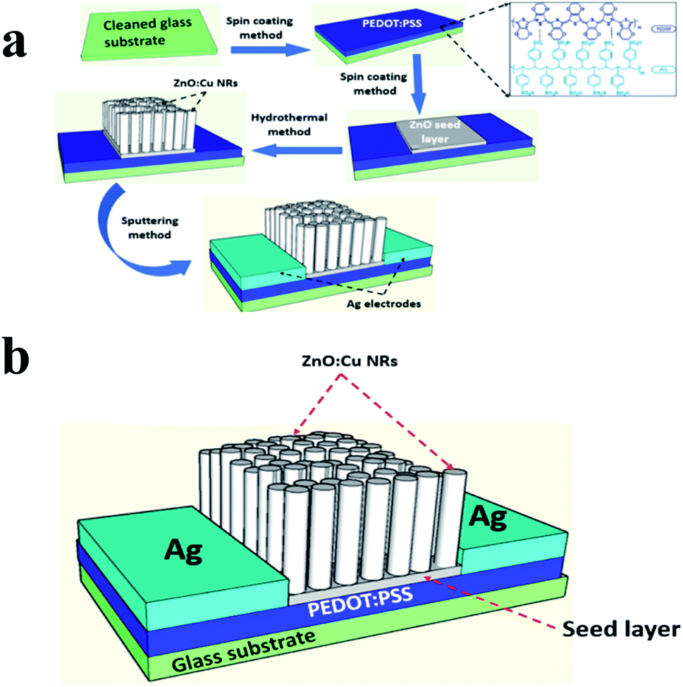 | ||
| Fig. 1 (a) The fabrication process of the hybrid photodetector. (b) The ultimate structure of the device. | ||
Materials optimization
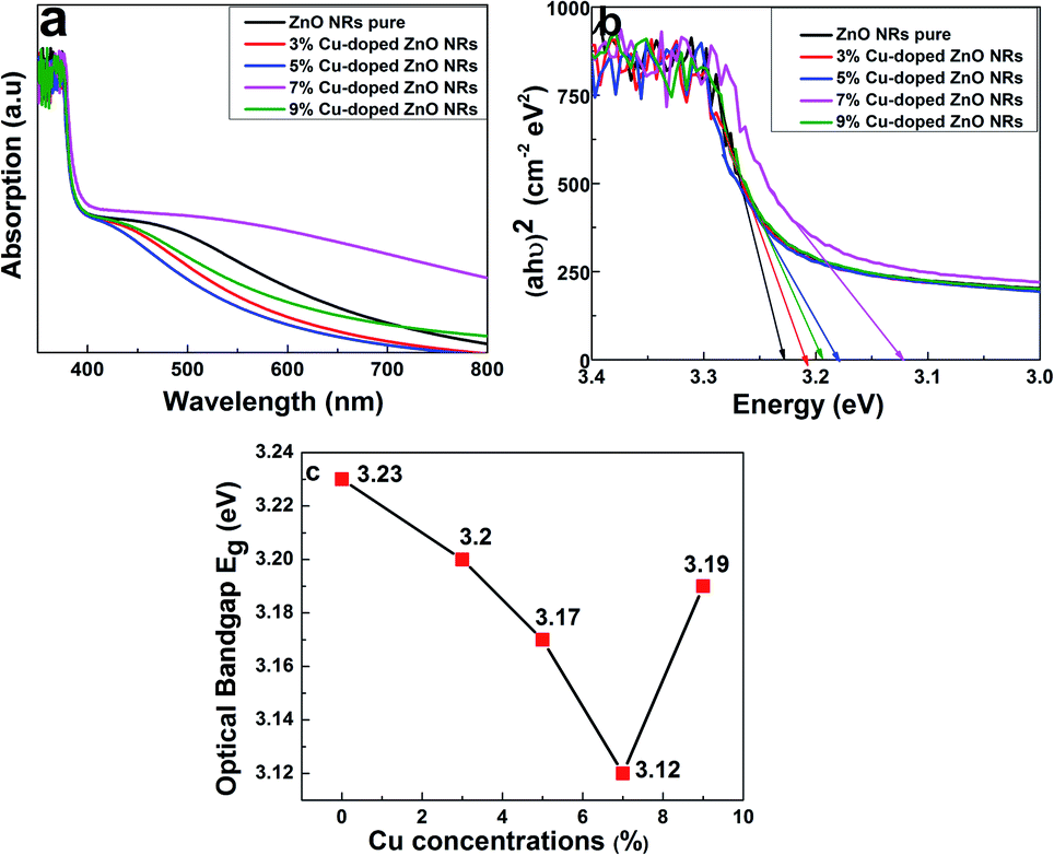 | ||
| Fig. 2 (a) UV-Vis spectra of ZnO NRs and Cu doping at different concentrations. (b) Plot of (αhν)2 versus energy, and the extrapolation of the linear parts of ZnO. (c) Optical bandgap of pure and Cu-doped ZnO NRs at different concentrations. | ||
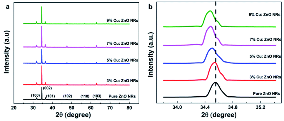 | ||
| Fig. 3 (a) XRD patterns of the undoped and Cu-doped ZnO nanorods. (b) Comparison of the (002) peaks taken for pure and Cu-doped ZnO NRs at different concentrations. | ||
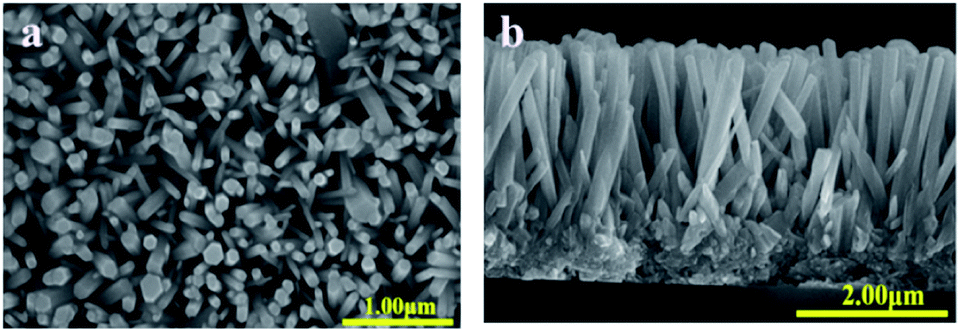 | ||
| Fig. 4 SEM images of Cu-doped ZnO NRs/PEDOT:PSS: (a) the top view, (b) the cross-section. | ||
Photodetector characteristics
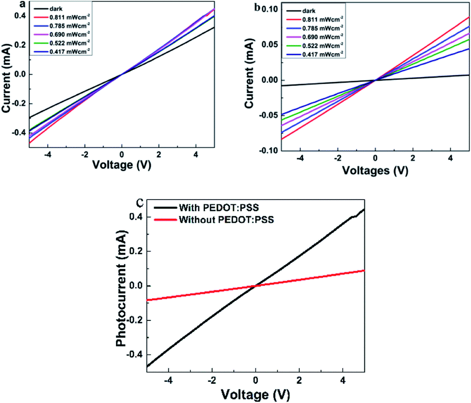 | ||
| Fig. 5 I–V characteristics of (a) Cu-doped ZnO NRs/PEDOT:PSS, (b) Cu-doped ZnO NRs photodetectors under 395 nm light illumination, and (c) the photocurrent of the samples with and without PEDOT:PSS under 395 nm light exposure with a photon intensity of 0.811 mW cm−2. | ||
To deeply understand the performance of photodetectors, current–times (I–t) characteristic measurement was conducted. The time-resolved photoresponse of the photodetector with and without the transport layer at a bias of 5 V is shown in Fig. 6. Both devices showed the increase in photocurrent under visible light illumination and the decay ability when the light was turned off. It was attributed to the generation of electron–hole pairs under light exposure. Indeed, when ZnO:Cu NRs absorbed the photons with an energy higher than the optical band gap, valence electrons lifted to the conduction band to become the conductance electrons and left behind the holes in the valence band. Consequently, electron–hole pairs were generated inside ZnO:Cu NRs leading to the increase in the photocurrent, which is discussed in more detail in the mechanism part. With different light intensities, the photocurrent values went up when P climbed (Fig. 6a and b). This result is explained by the relationship between photocurrent and light intensity,41 Iphoto = APθ, where A is the wavelength constant and θ is the exponential. At an incident illumination of 0.811 mW cm−2, the photocurrent reached 0.269 mA for the sample with PEDOT:PSS, while the corresponding value without hole transport layer was 0.110 mA. This matched with the I–V characteristic, which has been given above.
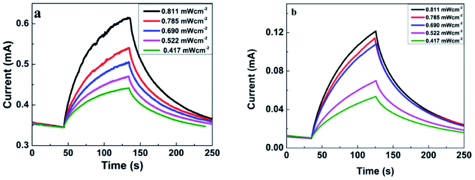 | ||
| Fig. 6 Time-resolved photocurrent response under 395 nm illumination with 5 V bias of the devices (a) with PEDOT:PSS and (b) without PEDOT:PSS. | ||
Two important parameters in a photodetector are responsivity (R) and photoconductive gain (G). Therefore, to determine the device performance, R and G should be calculated from I–V and I–t curves. The responsivity was defined by the ratio of generated photocurrent to illumination intensity, and it could be calculated using the formula42
where h was Planck's constant, c represented the velocity of light, 3 × 10⁸ ms−1, λ was the light wavelength, e was the electron charge, and R was the responsivity of the photodetector, τlife was the lifetime, μ: mobility of carriers, and L was the distance between electrodes. Under the same illuminating condition (wavelength of 395 nm and light intensity of 0.811 mW cm−2), the responsivity of the device with hole transport layer was 0.33 A W−1, nearly 2.36 times higher than that without transport layer (0.14 A W−1). The photoconductive gain of the device with PEDOT:PSS was 1.036, a twofold value compared to that without PEDOT:PSS (0.439) (Table 1). One explanation was that G depended on the charge carrier mobility, and thus, the higher the mobility, the higher the photoconductive gain.43,44
| Active materials | λ (nm) | Iph (mA) | Response time (s) | Recovery time (s) | R (A W−1) | Bias | Reference |
|---|---|---|---|---|---|---|---|
| ZnO NRs | 365 | 0.36 | 25.74 | 36.73 | 0.87 | 5 | 56 |
| ZnO NRs | 365 | 0.308 | 38.10 | 3.66 | — | — | 57 |
| Cu-doped ZnO NRs | 380 | 0.89 | 58 | 83 | — | 3 | 39 |
| Mn doped ZnO NRs/PEDOT:PSS | 365 | — | 2.75 | 16.8 | 0.065 | 5 | 58 |
| ZnO@CdS/PEDOT:PSS | 470 | 1.4 × 10⁻³ | ∼0.02 | ∼0.02 | — | 0 | 59 |
| AZO/ZnO/PVK/PEDOT:PSS | 365 | — | 0.11 | 0.2 | 0.081 | 5 | 60 |
| ZnO NRs/GQD/PEDOT:PSS | 340 | ∼15 | — | — | 36 | −1 | 28 |
| Single crystal ZnO/PEDOT:PSS | 370 | 3.5 × 10⁻⁶ | — | — | 0.3 | — | 61 |
| Cu-doped ZnO NRs | 395 | 0.1145 | 36.41 | 48.3 | 0.14 | 5 | This work |
| Cu-doped ZnO NRs/PEDOT:PSS | 395 | 0.2704 | 28.21 | 42.01 | 0.33 | 5 | This work |
Fig. 7a presents the response time and recovery time of the photodetector based on ZnO:Cu NRs with and without PEDOT:PSS. Following other reports, response time was defined as the time to reach 63% of the photocurrent response from the start of the illumination, while recovery time was calculated as the time to reach 37% of photocurrent after turning off the light.45,46 The hybrid photodetector exhibited a response time of 28.21 s, faster than that of Cu-doped ZnO NRs (36.41 s). This was because the mobility of PEDOT:PSS was higher than that of ZnO:Cu NRs. To investigate the stability of the device, the reversible switching between high and low currents was denoted in Fig. 7b, where the incident light was turned on and off repeatedly. It could be clearly seen that slight changes in sensing performance after four repetitions of switching between the light on and off state demonstrated good stability of our device.
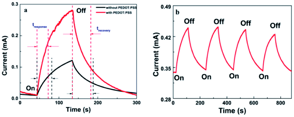 | ||
| Fig. 7 I–t curves of the device (a) with and without PEDOT:PSS in 1 cycle, and (b) with PEDOT:PSS in 4 continuous cycles. | ||
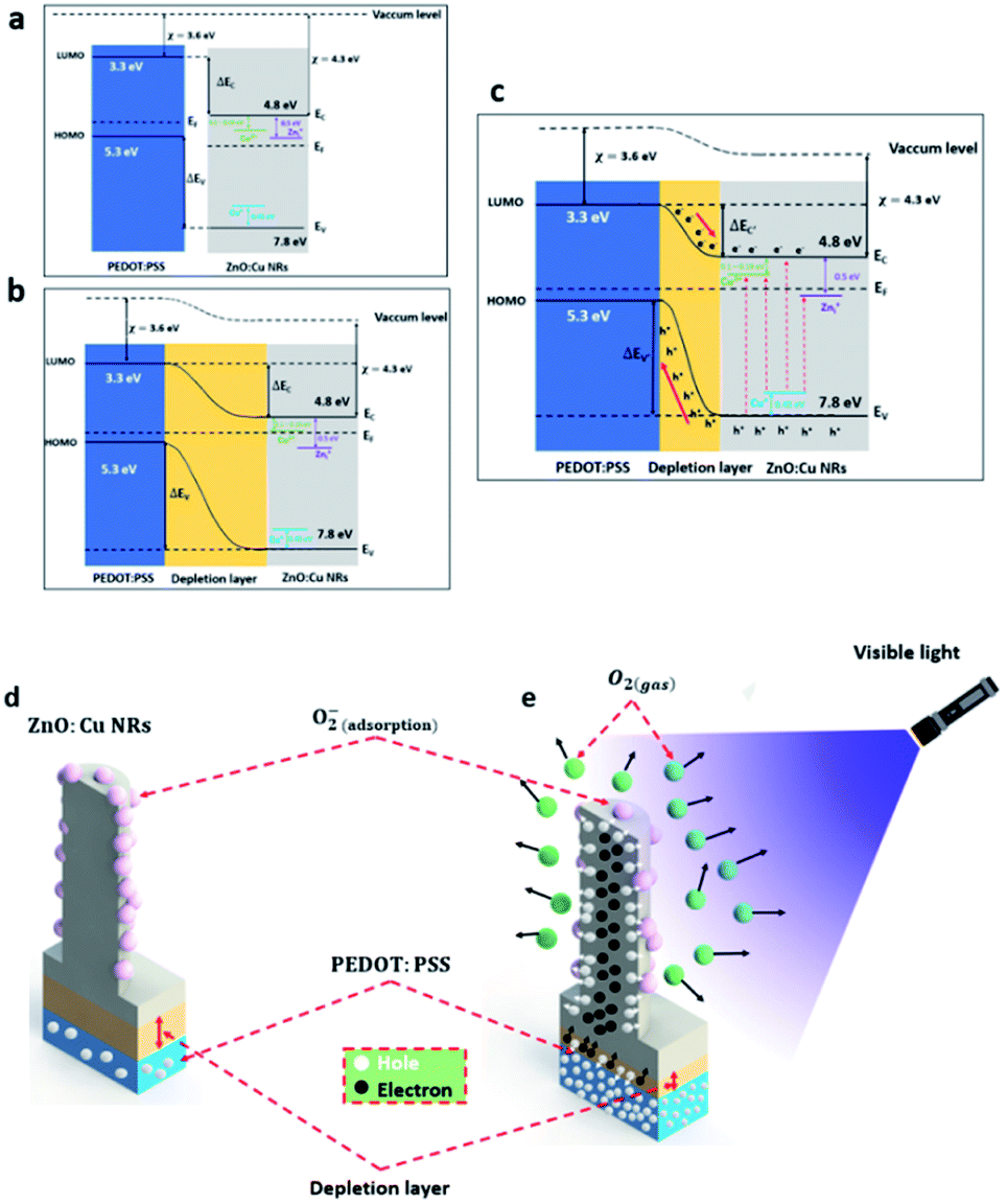 | ||
| Fig. 8 (a) The energy diagram of ZnO:Cu NRs and PEDOT:PSS before contact. (b) Schematic illustration of the energy band structure of ZnO:Cu NRs/PEDOT:PSS heterojunction in dark conditions. (c) The electron–hole pair generation and transmission process under visible illumination. The schematic diagram of the visible photodetector with the ZnO:Cu NRs/PEDOT:PSS heterojunction (d) under dark conditions and (e) visible illumination. | ||
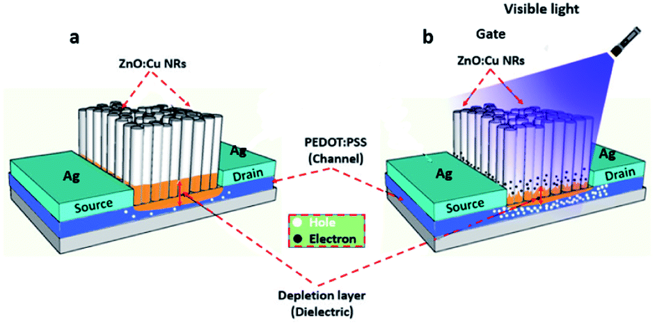 | ||
| Fig. 9 Schematic diagrams of the visible photodetector considered as a vertical transistor with a photogating effect under (a) dark conditions and (b) light illumination. | ||
Comparing the performance of these PDs to the different research studies, the proposed device showed superior performances of photocurrent and responsivity. As shown in Table 1, the values of response time, recovery time, R, and G have been enhanced. Thus, the structure of this device has reached the theoretical suggestions. In addition, the response and recovery times of the device can be improved by boosting either the crystallinity of ZnO nanorods54 or the mobility of the carrier transport layer,55 which will be conducted in our following study. Although the performance of our device was relatively low, it was still higher than that in some other reports, which meant that our results were acceptable for some realistic applications.
Conclusions
In summary, we successfully synthesized a hybrid material between Cu-doped ZnO NRs and PEDOT:PSS on a glass substrate. The performance of the hybrid photodetector was enhanced due to the high mobility of the hole transport layer. With 7% Cu doping, the hybrid photodetector responded to the visible light with a wavelength of 395 nm. The responsivity of the hybrid photodetector was 0.33 A W−1, higher than that of ZnO:Cu NRs photodetector (0.14 A W−1). The device with the transport layer also showed fast response and recovery times with values of 28.21 s and 42.01 s, respectively. These suggest that our device has the potential for further applications in the future.Conflicts of interest
There are no conflicts to declare.Acknowledgements
This research is funded by Thu Dau Mot University, Binh Duong Province, Vietnam under grant number DT.21.1-030.Notes and references
- J. Haas, M. Schwartz, U. Rengstl, M. Jetter, P. Michler and B. Mizaikoff, Analyst, 2018, 143, 593–605 RSC.
- F. Li, C. Ma, H. Wang, W. Hu, W. Yu, A. D. Sheikh and T. Wu, Nat. Commun., 2015, 6, 1–8 Search PubMed.
- Y. Cui, H. Yao, L. Hong, T. Zhang, Y. Xu, K. Xian, B. Gao, J. Qin, J. Zhang and Z. Wei, Adv. Mater., 2019, 31, 1808356 CrossRef PubMed.
- Z. Zhou, Y. Li, M. Xia, Y. Zhong, N. Zhou and H. T. Hintzen, Dalton Trans., 2018, 47, 13713–13721 RSC.
- K. Yamamoto, T. Oguchi, K. Sasaki, I. Nomura, S. Uzawa and K. Hatanaka, J. Soc. Inf. Disp., 2006, 14, 73–79 CrossRef CAS.
- X.-Y. Wang, A. L. Fitch, H. H. C. Iu, V. Sreeram and W.-G. Qi, Chin. Phys. B, 2012, 21, 108501 CrossRef.
- H. M. Günther, T. Birnstiel, D. P. Huenemoerder, D. A. Principe, P. C. Schneider, S. J. Wolk, F. Dubois, L. Logie, S. Rau and S. Vanaverbeke, Astron. J., 2018, 156, 56 CrossRef.
- P. Ma, N. Flöry, Y. Salamin, B. Baeuerle, A. Emboras, A. Josten, T. Taniguchi, K. Watanabe, L. Novotny and J. Leuthold, ACS Photonics, 2018, 5, 1846–1852 CrossRef CAS.
- R. D. Hudson and J. W. Hudson, Proc. IEEE, 1975, 63, 104–128 Search PubMed.
- Z. Zhao, J. Liu, Y. Liu and N. Zhu, J. Semicond., 2017, 38, 121001 CrossRef.
- F. Huang, F. Jia, C. Cai, Z. Xu, C. Wu, Y. Ma, G. Fei and M. Wang, Sci. Rep., 2016, 6, 28943 CrossRef CAS PubMed.
- S. Youssef, Y. M. El-Batawy and A. A. Abouelsaood, J. Appl. Phys., 2016, 120, 124506 CrossRef.
- M. Wang, F. Ren, G. Cai, Y. Liu, S. Shen and L. Guo, Nano Res., 2014, 7, 353–364 CrossRef CAS.
- M. W. Zhu, N. Huang, J. Gong, B. Zhang, Z. J. Wang, C. Sun and X. Jiang, Appl. Phys. A, 2011, 103, 159–166 CrossRef CAS.
- A. Bera and D. Basak, Appl. Phys. Lett., 2009, 94, 163119 CrossRef.
- M. Chakraborty, A. Ghosh and R. Thangavel, J. Sol-Gel Sci. Technol., 2015, 74, 756–764 CrossRef CAS.
- D. Li, Z. T. Liu, Y. H. Leung, A. B. Djurišić, M. H. Xie and W. K. Chan, J. Phys. Chem. Solids, 2008, 69, 616–619 CrossRef CAS.
- J. Lermé, J. Phys. Chem. C, 2011, 115, 14098–14110 CrossRef.
- A. K. Dikshit, S. Maity, N. Mukherjee and P. Chakrabarti, IEEE J. Photovolt, 2021, 11, 983–990 Search PubMed.
- S. Maity, B. Das, R. Maity, N. P. Maity, K. Guha and K. Srinivasa Rao, Sol. Energy, 2019, 185, 439–444 CrossRef CAS.
- S. Maity and T. Thomas, IEEE Trans. Electron Devices, 2018, 65, 4548–4554 CAS.
- Y. Li, G. W. Meng, L. D. Zhang and F. Phillipp, Appl. Phys. Lett., 2000, 76, 2011–2013 CrossRef CAS.
- S. Y. Bae, C. W. Na, J. H. Kang and J. Park, J. Phys. Chem. B, 2005, 109, 2526–2531 CrossRef CAS PubMed.
- A. Ghosh, A. Ghule and R. Sharma, J. Phys.: Conf. Ser., 2012, 365, 012022 CrossRef.
- X. Zhang, J. Zhang, B. Leng, J. Li, Z. Ma, W. Yang, F. Liu and B. Liu, Adv. Mater. Interfaces, 2019, 6, 1901365 CrossRef CAS.
- K.-L. Chu, C.-H. Chen, S.-W. Shen, C.-Y. Huang, Y.-X. Chou, M.-Y. Liao, M.-L. Tsai, C.-I. Wu and C.-C. Chueh, Chem. Eng. J., 2021, 422, 130112 CrossRef CAS.
- X. Zhang, J. Li, W. Yang, B. Leng, P. Niu, X. Jiang and B. Liu, ACS Appl. Mater. Interfaces, 2019, 11, 24459–24467 CrossRef CAS PubMed.
- S. Dhar, T. Majumder and S. P. Mondal, ACS Appl. Mater. Interfaces, 2016, 8, 31822–31831 CrossRef CAS PubMed.
- C. Xie and F. Yan, J. Mater. Chem. C, 2018, 6, 1338–1342 RSC.
- C. H. N. Van, H. K. Nguyen, H. Q. Huynh, H. A. Pham, T. M. Dinh, H. N. Luong, B. T. Phan, C. K. Tran and V. Q. Dang, Adv. Nat. Sci: Nanosci. Nanotechnol., 2020, 11, 015002 CAS.
- N. R. Yogamalar and A. Chandra Bose, Appl. Phys. A, 2011, 103, 33–42 CrossRef CAS.
- Z. Banu Bahşi and A. Y. Oral, Opt. Mater., 2007, 29, 672–678 CrossRef.
- B. D. Viezbicke, S. Patel, B. E. Davis and D. P. Birnie, Phys. Status Solidi B, 2015, 252, 1700–1710 CrossRef CAS.
- Y. Ji, U. Jung, Z. Xian, D. Kim, J. Yu and J. Park, Sens. Actuators, A, 2020, 304, 111876 CrossRef CAS.
- K. Omri, A. Bettaibi, K. Khirouni and L. El Mir, Phys. B, 2018, 537, 167–175 CrossRef CAS.
- F. Yang, S. Ma, X. Zhang, M. Zhang, F. Li, J. Liu and Q. Zhao, Superlattices Microstruct., 2012, 52, 210–220 CrossRef CAS.
- B. Nie, J.-G. Hu, L.-B. Luo, C. Xie, L.-H. Zeng, P. Lv, F.-Z. Li, J.-S. Jie, M. Feng, C.-Y. Wu, Y.-Q. Yu and S.-H. Yu, Small, 2013, 9, 2872–2879 CrossRef CAS PubMed.
- H. Q. Huynh, K. N. Pham, B. T. Phan, C. K. Tran, H. Lee and V. Q. Dang, J. Photochem. Photobiol., A, 2020, 399, 112639 CrossRef CAS.
- Y.-L. Chu, L.-W. Ji, H.-Y. Lu, S.-J. Young, I.-T. Tang, T.-T. Chu, J.-S. Guo and Y.-T. Tsai, J. Electrochem. Soc., 2020, 167, 027522 CrossRef CAS.
- M. Salah, S. Azizi, A. Boukhachem, C. Khaldi, M. Amlouk and J. Lamloumi, J. Mater. Sci., 2017, 52, 10439–10454 CrossRef CAS.
- H. Zhang, X. Zhang, C. Liu, S.-T. Lee and J. Jie, ACS Nano, 2016, 10, 5113–5122 CrossRef CAS PubMed.
- H. N. Pham, M. H. Tong, H. Q. Huynh, H. D. Phan, C. K. Tran, B. T. Phan and V. Q. Dang, Sens. Actuators, A, 2020, 311, 112085 CrossRef CAS.
- Z. Bai, X. Chen, X. Yan, X. Zheng, Z. Kang and Y. Zhang, Phys. Chem. Chem. Phys., 2014, 16, 9525–9529 RSC.
- Z. Bai, X. Yan, X. Chen, H. Liu, Y. Shen and Y. Zhang, Curr. Appl. Phys., 2013, 13, 165–169 CrossRef.
- S. Sarkar and D. Basak, Appl. Phys. Lett., 2013, 103, 041112 CrossRef.
- L. Zhu, Q. Dai, Z.-F. Hu, X.-Q. Zhang and Y.-S. Wang, Opt. Lett., 2011, 36, 1821–1823 CrossRef CAS PubMed.
- Y. Zhang, J. Xu, S. Shi, Y. Gao, X. Zhao, C. Wei, X. Zhang and L. Li, Nanotechnology, 2017, 28, 415202 CrossRef PubMed.
- C. S. Pathak, J. P. Singh and R. Singh, Curr. Appl. Phys., 2015, 15, 528–534 CrossRef.
- V. Q. Dang, T. Q. Trung, D.-I. Kim, L. T. Duy, B.-U. Hwang, D.-W. Lee, B.-Y. Kim, L. D. Toan and N.-E. Lee, Small, 2015, 11, 3054–3065 CrossRef CAS PubMed.
- V. Q. Dang, T. Q. Trung, L. T. Duy, B.-Y. Kim, S. Siddiqui, W. Lee and N.-E. Lee, ACS Appl. Mater. Interfaces, 2015, 7, 11032–11040 CrossRef CAS PubMed.
- Z. Xian-Li and Z. Rong, Chin. Phys. B, 2015, 24, 107703 CrossRef.
- A. Kumar, S. Ratan, D. K. Jarwal, A. K. Mishra, C. Kumar, A. P. Singh, B. Mukherjee and S. Jit, Mater. Res. Express, 2019, 6, 115514 CrossRef CAS.
- T. Q. Trung, V. Q. Dang, H.-B. Lee, D.-I. Kim, S. Moon, N.-E. Lee and H. Lee, ACS Appl. Mater. Interfaces, 2017, 9, 35958–35967 CrossRef CAS PubMed.
- B. Nie, J.-G. Hu, L.-B. Luo, C. Xie, L.-H. Zeng, P. Lv, F.-Z. Li, J.-S. Jie, M. Feng and C.-Y. Wu, Small, 2013, 9, 2872–2879 CrossRef CAS PubMed.
- S. A. Rutledge and A. S. Helmy, J. Appl. Phys., 2013, 114, 133708 CrossRef.
- N. A. Hammed, A. A. Aziz, A. I. Usman and M. A. Qaeed, Ultrason. Sonochem., 2019, 50, 172–181 CrossRef CAS PubMed.
- F. Yi, Q. Liao, X. Yan, Z. Bai, Z. Wang, X. Chen, Q. Zhang, Y. Huang and Y. Zhang, Physica E Low Dimens. Syst. Physica E Low Dimens. Syst. Nanostruct., 2014, 61, 180–184 CrossRef CAS.
- C. O. Chey, X. Liu, H. Alnoor, O. Nur and M. Willander, Phys Status Solidi Rapid Res Lett ., 2015, 9, 87–91 CrossRef CAS.
- S. Sarkar and D. Basak, ACS Appl. Mater. Interfaces, 2015, 7, 16322–16329 CrossRef CAS PubMed.
- X. Zhang, J. Li, W. Yang, B. Leng, P. Niu, X. Jiang and B. Liu, ACS Appl. Mater. Interfaces, 2019, 11, 24459–24467 CrossRef CAS PubMed.
- M. Nakano, T. Makino, A. Tsukazaki, K. Ueno, A. Ohtomo, T. Fukumura, H. Yuji, S. Akasaka, K. Tamura, K. Nakahara, T. Tanabe, A. Kamisawa and M. Kawasaki, Appl. Phys. Lett., 2008, 93, 123309 CrossRef.
| This journal is © The Royal Society of Chemistry 2021 |