DOI:
10.1039/D1RA05840A
(Paper)
RSC Adv., 2021,
11, 34048-34058
Two-dimensional polarized MoTe2/GeS heterojunction with an intrinsic electric field for photocatalytic water-splitting†
Received
1st August 2021
, Accepted 29th September 2021
First published on 20th October 2021
Abstract
The construction of van der Waals heterostructures based on 2D polarized materials is a unique technique to achieve enhanced photocatalytic performance. We have investigated the intrinsic electric field and photocatalytic properties of the MoTe2/GeS heterostructure via first-principles calculations. The results showed that a dipole-induced electric field induced by the GeS monolayer and an interface-induced electric field induced by the interface between the GeS monolayer and the MoTe2 monolayer emerge in the 2D polarized MoTe2/GeS heterostructure. The dipole-induced electric field contributes mainly to the total intrinsic electric field. Moreover, the 2D polarized MoTe2/GeS heterostructure possesses many excellent and distinguished photocatalytic performance parameters, such as a direct semiconductor bandgap of 1.524 eV, a wide light spectrum ranging from the ultraviolet to near-infrared region with a high absorption coefficient (about 106 cm−1), a total intrinsic electric field, which reduces the probability of the recombination of photo-generated electron–hole pairs effectively, and a suitable band alignment for the water-splitting reaction. These indicate that the 2D polarized MoTe2/GeS van der Waals heterostructure is a potential novel high-efficient photocatalyst for water-splitting.
1. Introduction
Due to the continuous high consumption of fossil fuels, humans have been facing energy crisis and the serial effects of environmental pollution.1–4 Therefore, many fossil fuels should be replaced by renewable and clean energy, such as solar energy. Photocatalytic water splitting is an attractive technology that converts solar energy into hydrogen energy and possesses some unique advantages, such as the consumption of only solar energy instead of fossil fuels. Moreover, O2 and H2 can be obtained continuously under solar light. Lastly, this technology is clean and does not pollute the environment.5–8 Therefore, this technology is considered a potential, feasible and efficient method to solve the environmental problems and the serious energy crisis at the same time.9–11 Since Fujishima reported this technology for the first time in 1972,12 photocatalytic water splitting has attracted a lot of attention around the world. Many materials, such as TiO2 (ref. 13–17) and SrTiO3,18–20 have been reported as potential catalysts in this process. However, the efficiency of common materials in converting solar energy into hydrogen energy is still unsatisfactory and low, owing to their low solar-light-absorption efficiency and high carrier recombination rates.21–24 In the process of solar energy to hydrogen energy conversion, solar-light absorption and carrier separation are the most important factors to improving the conversion efficiency. Moreover, the band alignments of catalysts should agree well with the redox potential; that is, the oxidation potential should be higher than the valence band maximum (VBM), and the reduction potential should be lower than the conduction band minimum (CBM) at the same time for the reaction of water splitting. However, these criteria are hardly met simultaneously due to the interaction between them.25
Recently, some researches have revealed that two-dimensional (2D) polarized materials, which possess a vertical intrinsic electric field induced by the dipole moment, show promising excellent properties for photocatalytic water splitting.26–30 On the one hand, the carriers can be transferred from the interior to the surface efficiently under the effect of the induced vertical intrinsic electric field. On the other hand, effective solar-light harvesting can be realized. Therefore, 2D polarized materials possess potential properties that satisfy the demands of simultaneous solar-light absorption and carrier separation necessary for photocatalytic water splitting. Many two-dimensional polarized materials have been reported as potential and effective photocatalysts for producing hydrogen energy based on theoretical and experimental findings.31–37 For instance, Yang et al. theoretically demonstrated that two-dimensional In2Te3, in which intrinsic electric field was experimentally attainable, can accomplish enhanced photocatalytic efficiency. Moreover, the theoretical efficiency even reached 32.1% on using the full solar spectrum.38 In our previous study, the dipole of monolayer GeSe and monolayer GeS has been demonstrated as a unique photocatalyst for water splitting owing to the dipole-induced electric field.39 Li et al. experimentally confirmed that GaN nanorod arrays possessed a distinguished advantage for charge separation due to the co-exposure of the polar and nonpolar surfaces, which induce an intrinsic electric field in the surface region. The charge-separation efficiency of the GaN nanorod arrays was 80%, which is much higher than the value (about 8%) of the GaN thin-film. Moreover, the quantum efficiency enhanced dramatically from 0.9% for the GaN thin-film to 6.9% for the GaN nanorod arrays.40 Zhang et al. also experimentally confirmed that multi-field coupling in KNbO3 nanostructures could enhance its catalytic performance owing to the polarization-modulated built-in electric fields, which effectively separated excited electron/hole pairs. The photocurrent density enhanced obviously from 25% for the nanocube counterpart to 55% for the KNbO3 nanosheets.41
van der Waals (vdW) heterojunctions based on two-dimensional materials can deliver better performance than isolated monolayers because the properties of isolated materials are complementary.42–48 Therefore, combining the different advantageous properties of different 2D materials to form vdW heterojunctions is an effective method to attain high-efficiency photocatalysts for water splitting. Moreover, the built-in electric field induced by the interface can effectively separate the excited carriers and enhance the photocatalytic activity.49–56 For example, Yuan and co-workers experimentally confirmed that the photocatalytic activity of 2D-2D MoS2/CdS,45 MoS2/g-C3N4 (ref. 57) and black phosphorus/MoS2 (ref. 58) could be enhanced by interface engineering, which allowed the charge carrier to be transferred and separated efficiently via abundant channels at the large 2D interfaces. Sun and co-workers experimentally reported that a 2D Janus heterojunction based on ZnIn2S4 and WO3 was a superior Z-scheme photocatalyst; it was helpful in boosting the separation of carriers, optimizing the charge lifetime and enhancing charge dynamics due to the effect of the internal electric field via the W–S bonds.59 Moreover, many theoretical studies, using the first-principles calculations method, have indicated that vdW heterojunctions, such as MoTe2/SnS2,48 blue phosphorene/BSe,43 BCN/C2N,46 MoS2/ZnO44 and C2N/WS2,49 are potential high-efficiency photocatalysts for water splitting. All the studies demonstrate the important role of the internal electric field of the vdW heterojunction in enhancing photocatalytic performance. Furthermore, polarized heterojunctions constructed based on two-dimensional polarized materials have been reported to possess a built-in electric field combined with not only an interface-induced electric field, but also a dipole-induced electric field.59–61 However, the effects of the dipole-induced electric field and interface-induced electric field in the vdW heterojunctions based on 2D polarized materials are not clear. It is very important to study and understand the coupling mechanism of the electric fields in 2D polarized vdW heterojunctions as it is key to designing highly efficient catalysts for photocatalytic water splitting.
In order to shed further light on universal strategies for constructing highly efficient 2D polarized vdW heterojunctions, we investigated the coupling effect of the dipole-induced electric field and interface-induced electric field in two-dimensional polarized materials, using MoTe2/GeS as the representative. The photocatalytic activity of the MoTe2/GeS vdW heterojunction was systematically investigated.
2. Computational methods
In this paper, all the calculations were performed using the Vienna ab initio simulation package (VASP);62 the Perdew–Burke–Ernzerhof (PBE) functional of the generalized gradient approximation (GGA) was considered for the exchange-correlation energy;63 the projector-augmented-wave (PAW) was used for electron–ion interactions;64 the optB88 method65,66 was adopted for the long-range vdW interactions of the MoTe2/GeS vdW heterojunction. To get a more accurate value, the bandgap was calculated by using the HSE06 hybrid functional.67 The energy cut-off was set to 500 eV for the plane-wave expansion of the wave function. To relax all the structures fully, the Hellmann Feynman force convergence and the energy convergence were set to 0.001 eV Å−1 and 10−6 eV, respectively. In order to exclude the artificial interactions, the thickness of the vacuum region was set to more than 20 Å along the Z direction. The gamma center schemes of 8 × 8 × 1 and 11 × 11 × 1 were used to sample the first Brillouin zone integration68 for geometry relaxation and static calculations, respectively.
The energy alignment of the MoTe2/GeS vdW heterojunction was calculated according to the method reported for polarized materials;26,28,38 the VBM energy level was obtained by the following equation:
in which the electrostatic potential in a vacuum is represented by
φ(∞), and the Fermi energy level corresponds to
EF. The CBM energy level was calculated in accordance with the following equation:
where
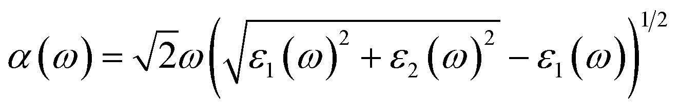
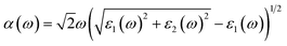
Egap is the bandgap calculated by the HSE06 hybrid functional. The dielectric function was calculated according to
eqn (3) to obtain the absorption spectrum.
69–71| |
 | (3) |
in which
α(
ω) is the absorption coefficient, and
ε1(
ω) and
ε2(
ω) are the real and imaginary parts of the frequency-dependent complex dielectric function, respectively.
3. Results and discussion
3.1 Structure of the MoTe2/GeS vdW heterojunction
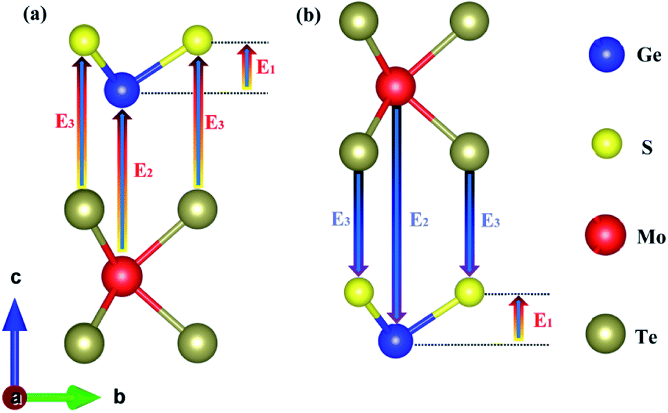
In order to construct the 2D polarized MoTe2/GeS vdW heterojunction, the GeS monolayer and MoTe2 monolayer were fully optimized first. The optimized lattice constants of the GeS monolayer and the MoTe2 monolayer were 3.495 Å and 3.550 Å, respectively, which were consistent with previous studies.39,72,73 It can be seen that the lattice mismatch, which was calculated from the difference in lattice constants between the GeS monolayer and the MoTe2 monolayer, was about 1.5%. The lattice mismatch was in an acceptable range, indicating that it was possible to form a vertical vdW heterojunction along the Z-axis between the GeS monolayer and the MoTe2 monolayer. As shown in Fig. 1, four possible stackings were considered, namely A1-, A2- and B1-, B2-stackings, to form the 2D polarized MoTe2/GeS vdW heterojunction. In the A1- and A2-stackings, the heterojunctions were formed based on the Ge–Te interface, in which the Ge atomic surface of the GeS monolayer approached the Te atomic surface of the MoTe2 monolayer. In contrast, the heterojunctions of the B1- and B2-stackings were formed based on the S–Te interface, in which the S atomic surface of the GeS monolayer approached the Te atomic surface of the MoTe2 monolayer. To obtain a stable heterojunction, all four stackings were fully optimized. The relationship between the lattice constant and the total energy of the MoTe2/GeS vdW heterojunction was calculated. As shown in Fig. S1,† the energy of the MoTe2/GeS vdW heterojunction was varied as the lattice constant was tuned, and the minimum value indicated the most stable structure. Therefore, in order to analyse the differences among the four stacking prototypes, the lattice constants were all taken as 3.554 Å.
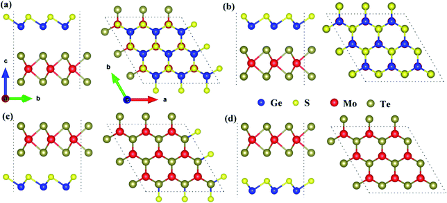 |
| | Fig. 1 Four prototype stacking structures of the MoTe2/GeS heterojunctions: (a)–(d) side and top views of A1-, A2-, B1- and B2-stackings, respectively. | |
3.2 The total intrinsic electric field of the MoTe2/GeS heterojunction
Because the electronegativities of atoms are different in two-dimensional polarized materials, the dipole-induced electric field induced by the GeS monolayer and the interface-induced electric field induced by the interface between GeS monolayer and MoTe2 monolayer emerged in the 2D polarized MoTe2/GeS vdW heterojunction. The total intrinsic electric field was composed of the dipole-induced electric field and the interface-induced electric field. As shown in Fig. 2, A2-stacking and B2-stacking were used as the models to study the coupling effect between the dipole-induced electric field and interface-induced electric field in the polarized MoTe2/GeS vdW heterojunction. The dipole-induced electric fields in all the stacking orders were almost the same because they were induced by the same GeS monolayer, and the electric fields were along the Z direction. In contrast, the isolated MoTe2 layer did not possess a similar electric field due to the symmetrical structure of the monolayer. When the GeS monolayer and the MoTe2 monolayer were stacked vertically to form the MoTe2/GeS vdW heterojunction, two different interfaces (the Ge–Te interface and the S–Te interface) were considered because of the electric field in the GeS monolayer along the Z direction. Both the atomic interfaces were not symmetrical, indicating that a new intrinsic dipole would be induced due to the different electronegativity values of the two atoms. Therefore, there would be an interface-induced electric field through the Ge–Te interface or the S–Te interface in the polarized MoTe2/GeS vdW heterojunction. Moreover, since the electric field is closely related to the interlayer distance, only the atoms in contact with each other were considered. The total intrinsic electric field E in the two-dimensional polarized vdW heterojunction can be expressed as:in which Ep is the dipole-induced electric field, and Ei is the interface-induced electric field. There was no electric field in the isolated MoTe2 layer, and the dipole-induced electric field of heterojunction was only contributed by the GeS layer (represented by E1); therefore, it is obvious that Ep was equal to E1. In contrast, the interface-induced electric field in the Ge–Te interface was different from that in the S–Te interface due to the difference in the electronegativity of the atoms. For example, the electronegativity of the Mo atom is greater than the electronegativity of the Ge atom, which would induce a built-in electric field at the interface, in the direction from the Mo-atom layer to the Ge-atom layer (represented by E2). Similarly, the electronegativity of the Te atom is greater than that of the S atom, inducing a built-in electric field at the interface, in the direction from the Te atomic layer to the S atomic layer (represented by E3). Therefore, Ei can be expressed as the vectorial sum of E2 and E3.
 |
| | Fig. 2 The coupling of the dipole-induced electric field and the interface-induced electric field in the polarized MoTe2/GeS vdW heterojunction based on (a) the Ge–Te interface and (b) the S–Te interface. | |
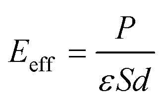
In this paper, the Z-axis was selected as the positive direction; then, the total intrinsic electric field (EA) of the polarized MoTe2/GeS vdW heterojunction based on the Ge–Te interface (A-stacking) was expressed as the vectorial sum of E1, E2 and E3. Similarly, the total intrinsic electric field (EB) of the polarized MoTe2/GeS vdW heterojunction based on the Ge–Te interface (the B-stacking) was expressed as the vectorial sum of E1, E2 and E3. Significantly, in the B-stacking case, E1 was in the opposite direction to E2 and E3. In addition, the built-in electric field Eeff was mainly induced by the intrinsic dipole P in accordance with the following formula:
| |
 | (5) |
where the dielectric constant, surface area and distance between the atomic layers are expressed as
ε,
S and
d, respectively. This indicates that the built-in electric field is inversely proportional to the distance
d. The interlayer distance of GeS was small, and the atomic distance at the heterojunction interface was large, so
Ei (
i = 2 or 3) was much smaller than
Ep. Therefore, the relationship between
EA,
EB and
Ep was:
This indicated that EA and EB were mainly contributed by Ep and that the vector directions of EA and EB were consistent with that of Ep along the positive direction of the Z-axis.
The electronegativity of atoms located in the upper surface and lower surface were different. Therefore, the built-in electric field Eeff and a surface electrostatic potential difference ΔΦ were induced by the intrinsic dipole P between the upper and lower surfaces. Eeff and ΔΦ are the intrinsic characteristics of polarized materials, which can result in the separation and migration of photo-generated carriers and reduce the recombination rate of carriers effectively, thus enhancing the photocatalytic performance of the two-dimensional polarized materials. The relationship between the built-in electric field Eeff and the surface electrostatic potential difference ΔΦ can be expressed by the following formula:
where the elementary charge constant is expressed as
e, and
d is the distance between the atomic layers. It can be seen that Δ
Φ is directly proportional to
Eeff. The larger the surface electrostatic potential difference Δ
Φ, the larger was the induced electric field
Eeff. As shown in Fig. S2,
† the planar average potential of the isolated GeS monolayer and the isolated MoTe
2 monolayer in the different stacking structures of the MoTe
2/GeS vdW heterojunction were calculated. For the isolated GeS monolayer, there was a significant surface potential difference Δ
Φ, and the potential energy of the Ge atomic layer at the bottom was lower than the potential energy of the S atomic layer on the top, indicating that the direction of dipole-induced electric field (
Ep) was pointing from the Ge-atom layer at the bottom to the S-atom layer at the top. For the isolated MoTe
2 monolayer, the potential energies of the upper and lower surfaces were equal, and the surface potential difference was 0 eV because both the upper and lower surfaces were symmetrical Te atomic layers with the same electronegativity. It was worth noting that the Δ
Φs of the isolated GeS monolayer in the A1-, A2- and B1-stackings was 1.082 eV, and the Δ
Φ of the isolated GeS monolayer in the B2 stacking was 1.083 eV. All of them were almost the same, and the difference between them was negligible. Therefore, this indicated that the dipole-induced electric field (
E1) of all the four differently stacked heterojunctions was the same since
E1 was induced only by the same isolated GeS layer.
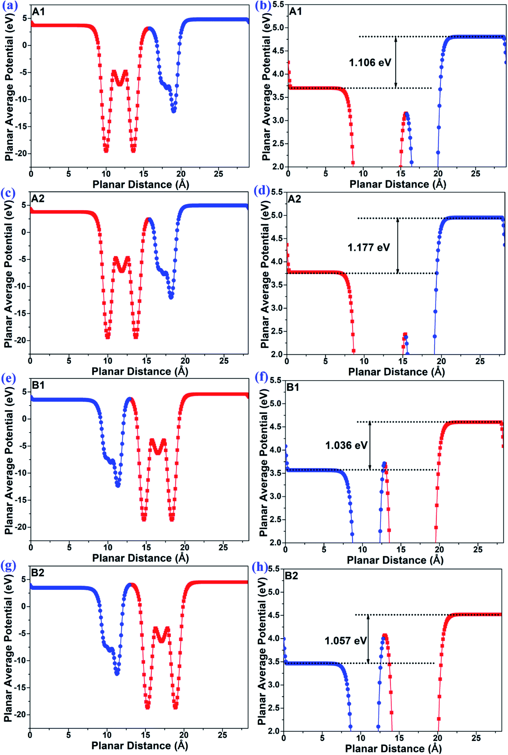
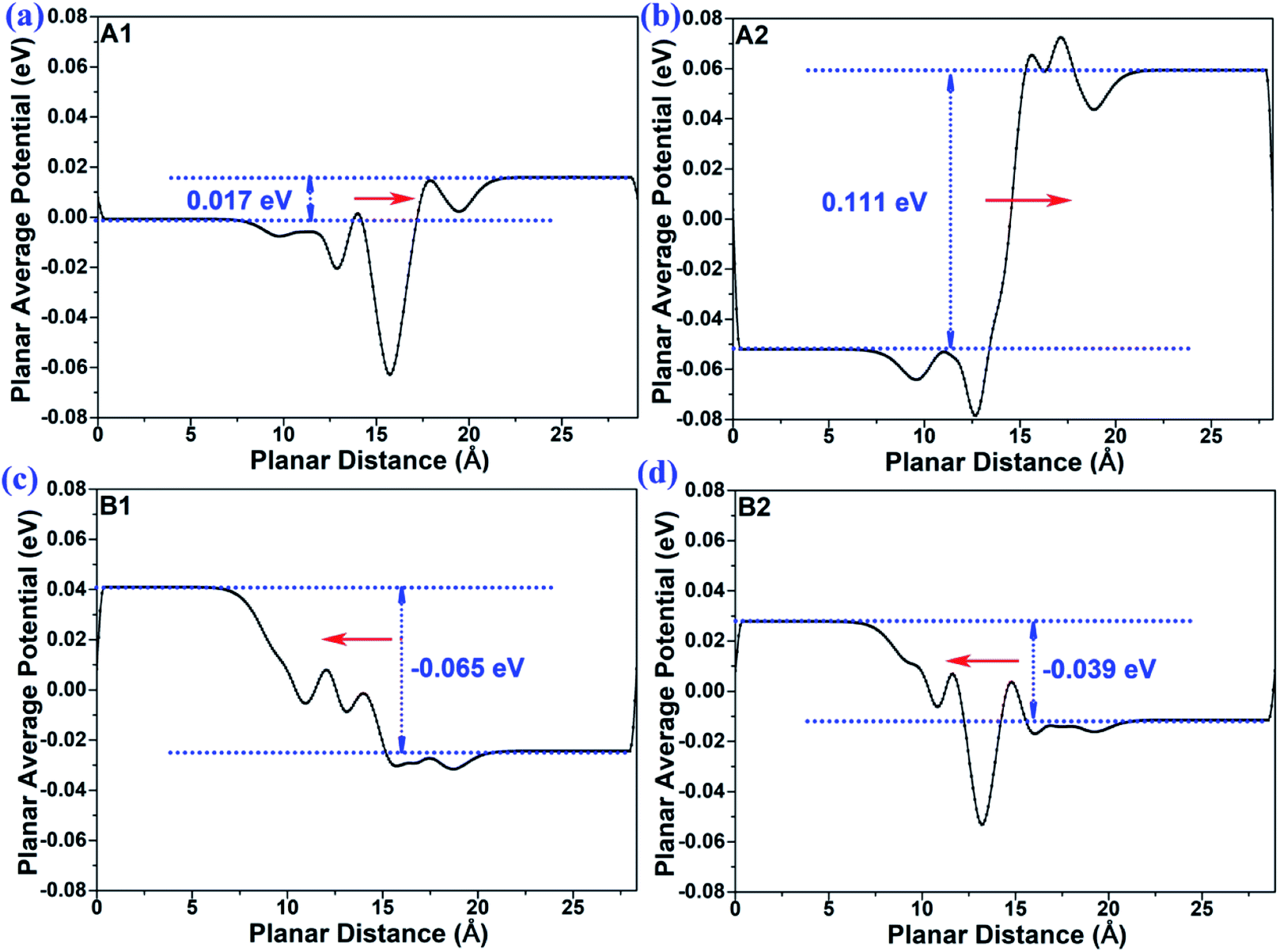
The planar average potentials of the MoTe2/GeS vdW heterojunction in the A1-, A2-, B1-, and B2-stacking configurations are shown in Fig. 3. All the stackings presented an obvious surface potential difference ΔΦ, and the potential energy at the bottom was lower than the potential energy at the top, indicating that the direction of the total intrinsic electric field (E) was along the Z direction, which is consistent with the direction of Ep of the GeS monolayer. Moreover, the interface-induced electric fields in the Ge–Te interfaces of the A1- and A2-stackings were different from those in the S–Te interfaces of the B1- and B2-stackings. However, the potential energy on the MoTe2 side was lower than that on the GeS side in the A1-, A2-, B1- and B2-stackings. This indicated that the total electric field of the heterojunction was mainly contributed by the dipole-induced electric field, while the interface-induced electric field was weaker.
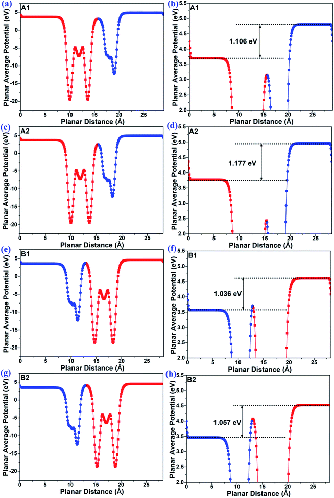 |
| | Fig. 3 The planar average potential of the MoTe2/GeS vdW heterojunction in (a) and (b) A1-, (c) and (d) A2-, (e) and (f) B1- and (g) and (h) B2-stackings. | |
As shown in Fig. 3, the ΔΦs of the MoTe2/GeS vdW heterojunctions in the A1-, A2-, B1-, and B2-stackings were 1.106 eV, 1.177 eV, 1.036 eV, and 1.057 eV, respectively, while that of the isolated GeS monolayer was 1.082 eV. It indicated that the total electric field of the heterojunction was mainly contributed by the dipole-induced electric field and suggested that the dipole-induced electric field was much larger than the interface-induced electric field. Moreover, it was found that
| | |
ΔΦ(B) < ΔΦ(GeS) < ΔΦ(A)
| (8) |
where Δ
Φ(B) and Δ
Φ(A) are, respectively, the surface potential differences of the B-type and A-type stacked heterojunctions, and Δ
Φ(GeS) is the surface potential difference of the GeS monolayer. The surface potential difference of the B-type stacked heterojunction was smaller than that of the GeS monolayer, while the surface potential difference of the A-type stacked heterojunction was larger compared with that of the GeS monolayer. This confirmed that the interface-induced electric field was different in the A-type and B-type stackings. In the A-type with the Ge–Te interface, the direction was along the
Z direction, while in B-type with the S–Te interface, the direction was along the −
Z direction. These results agree well with the analysis in
Fig. 2 mentioned above.
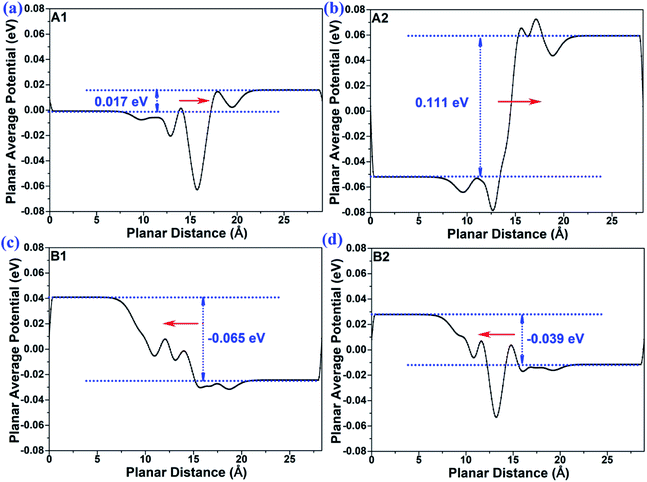
In order to provide insights into the mechanism of the interface-induced electric field, we calculated the planar average potential difference ΔP of the MoTe2/GeS vdW heterojunction by the following formula:
| | |
ΔP = Pheterostructure − PGeS − PMoTe2
| (9) |
where
Pheterostructure,
PGeS and
PMoTe2 are the planar average potentials of the MoTe
2/GeS vdW heterojunction, GeS monolayer and MoTe
2 monolayer, respectively. Δ
P was mainly contributed by the interface-induced electric field, indicating that the direction of Δ
P represented the direction of the interface-induced electric field. As shown in
Fig. 4, for the A1- and A2-stackings based on the Ge–Te interface, the direction of Δ
P was along the positive direction of the
Z-axis, indicating that the interface-induced electric field was directed from the bottom atomic layer to the top atomic layer. By contrast, for the B1- and B2-stackings based on the S–Te interface, the direction of Δ
P was along the negative direction of the
Z-axis, which indicated the interface-induced electric field was directed from the top atomic layer to the bottom atomic layer. Therefore, the interface-induced electric field was closely related to the stacking order based on the different interface structures. The direction of the interface-induced electric field was the same for the stackings based on the same interfaces. The results were consistent with the above-mentioned analysis
Fig. 2 and
3. Moreover, it was found that the value of the planar average potential difference (Δ
P), which represents the interface-induced electric field induced by the interface between the GeS monolayer and the MoTe
2 monolayer, was much smaller than the value of the surface potential difference of the GeS monolayer (Δ
Φ), which represents the dipole-induced electric field induced by the GeS monolayer. This confirmed that the total intrinsic electric field was mainly contributed by the dipole-induced electric field, while the interface-induced electric field contributed less to the total intrinsic electric field. Therefore, when the interface-induced electric field and the dipole-induced electric field are in the same direction, a larger total intrinsic electric field would be induced. Meanwhile, the total intrinsic electric field would be slightly smaller than the dipole-induced electric field when the interface-induced electric field and the dipole-induced electric field are in opposite directions.
 |
| | Fig. 4 The plane-average potential difference along the Z direction of MoTe2/GeS vdW heterojunction for (a) A1-, (b) A2-, (c) B1- and (d) B2-stacking. | |
3.3 Stability and phonon dispersion
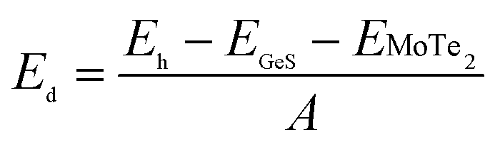
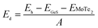
The coupling mechanism of the built-in dipole electric field and the interface-induced electric field of the different stacking sequences has been studied above. The A2-stacking structure possessed the largest total intrinsic electric field, which is useful to separate the photo-generated carriers, expand the solar light absorption region and enhance the performance of the photocatalytic water splitting. To obtain the most stable vdW heterojunction, all the four stacking structures were fully optimized, and the total energies of the different stacking structures were also calculated. As shown in Fig. 5(a), it was clear that the total energy of the A2-stacking was the minimum, while the B2- and A1-stackings possessed the maximum value, and the total energy of the B1-stacking was in between, indicating that the A2-stacking would be the most stable structure among the four. Therefore, the A2-stacking was taken as the optimum structure to discuss the properties of the MoTe2/GeS vdW heterojunction. To verify the thermodynamic and dynamical stability of the MoTe2/GeS vdW heterojunction, the binding energy Ed of the MoTe2/GeS heterojunction was calculated by the following formula:| |
 | (10) |
in which Eh, EMoTe2 and EGeS are the total energy corresponding to the MoTe2/GeS vdW heterojunction, isolated MoTe2 monolayer and isolated GeS monolayer, respectively. The interface area of the MoTe2/GeS vdW heterojunction is represented as A. According to the definition, the vdW heterojunction structure would be the most stable if the value of binding energy is the most negative. The value of binding energy of the MoTe2/GeS vdW heterojunction was about −48.34 meV Å−2, similar to those of other vdW heterojunctions.70,74–76 This confirmed that the MoTe2/GeS vdW heterojunction was thermodynamically stable. Moreover, the phonon spectrum of the vdW heterojunction with A2-stacking was calculated, as shown in Fig. 5(b); there was no obvious virtual frequency in the phonon spectrum, which confirmed its dynamical stability. Therefore, the A2-stacked vdW heterojunction was used as the representative to study the photocatalytic performance.
 |
| | Fig. 5 (a) Energy difference ΔEi (eV) between the optimized MoTe2/GeS vdW heterojunctions and the most stable heterojunction; (b) the phonon spectrum of the MoTe2/GeS vdW heterojunction. | |
3.4 Electronic properties
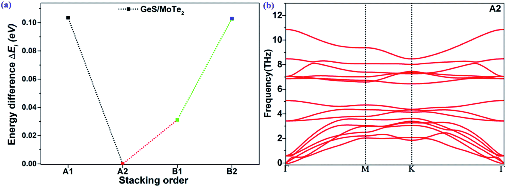
The band structures of the GeS monolayer, MoTe2 monolayer and MoTe2/GeS vdW heterojunction were calculated using the HSE06 method to get accurate values. As shown in Fig. 6(a), for the GeS monolayer, the valence band maximum (VBM) was located between K and Γ. As a contrast, the conduction band minimum (CBM) was located between Γ and M. The GeS monolayer was an indirect semiconductor with a bandgap of 3.265 eV, which is very large and similar to traditional bulk material catalysts, such as TiO2. This indicated that only a few ultraviolet light spectra, which is just about 5% of the full solar spectrum, would be absorbed and utilized by the GeS monolayer. Thus, the GeS monolayer possesses low solar-light absorption and low conversion efficiency in photocatalytic water splitting. As shown in Fig. 6(b), the MoTe2 monolayer was a direct semiconductor with the CBM and VBM located at the K point. The bandgap of the MoTe2 monolayer was 1.505 eV, which is consistent with previous results.77 Compared with the GeS monolayer, the MoTe2 monolayer possesses a direct semiconductor characteristic with a suitable value of bandgap for solar-light conversion and absorption of the visible light spectrum. This means that the MoTe2 monolayer is a potential material for solar spectrum utilization. As shown in Fig. 6(c), the MoTe2/GeS vdW heterojunction was also a direct semiconductor with the CBM and the VBM located at the K point. The bandgap of the MoTe2/GeS vdW heterojunction was 1.524 eV. The band structure of the MoTe2/GeS vdW heterojunction retained the individual band characteristics of the component monolayers. It was notable that the CBM and VBM were very similar to those of the MoTe2 monolayer, and therefore, the MoTe2/GeS vdW heterojunction maintained the direct bandgap semiconductor characteristics as the MoTe2 monolayer. Moreover, since the smaller bandgap of the MoTe2/GeS vdW heterojunction than that of the GeS monolayer suggested that light in a wider solar spectrum (including ultraviolet light and visible spectrum) would be absorbed effectively. Therefore, the construction of MoTe2/GeS vdW heterojunction is an effective way to solve the problem of low solar-light absorption in the GeS monolayer.
 |
| | Fig. 6 The band structures (HSE06) of the (a) GeS monolayer, (b) MoTe2 monolayer, (c) MoTe2/GeS vdW heterojunction. (d) The partial density of states (PDOS) of the MoTe2/GeS vdW heterojunction. | |
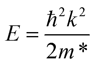
The effective mass m* of electrons and holes in the MoTe2 monolayer, GeS monolayer and MoTe2/GeS heterojunction were calculated by fitting the HSE06 band structures to a parabola, according to the following equation:
| |
 | (11) |
For the MoTe2 monolayer, the CBM and VBM were always located in K point, and the effective electron and hole masses were 0.635me and −0.752me, which were consistent with the values 0.58me and −0.74me reported in the previous studies.78 Here, the electron static mass is represented as me. For the GeS monolayer, the VBM was located between K and Γ, and the CBM was located between Γ and M; the effective electron and hole masses were 1.518me and −1.534me, respectively. Moreover, for the MoTe2/GeS vdW heterojunction, the CBM and VBM were always located at the K point, and the effective electron and hole masses were 0.723me and −0.825me, respectively. It was notable that the effective masses of electrons and holes in the MoTe2/GeS vdW heterojunction were between those of the MoTe2 monolayer and the GeS monolayer but closer to those of the MoTe2 monolayer because the MoTe2/GeS vdW heterojunction maintained the advantageous band structural characteristics of the MoTe2 monolayer.
In order to see the contribution of each element to the band structure of the MoTe2/GeS vdW heterojunction, the partial density of states (PDOS) of the MoTe2/GeS vdW heterojunction was calculated, as shown in Fig. 6(d). The CBM was mainly contributed by the d orbitals of the Mo atoms and the p orbitals of the Te atoms. In contrast, the VBM was mainly contributed by the d electrons of the Mo atoms. Therefore, the direct bandgap semiconductor characteristics of the MoTe2/GeS vdW heterojunction were mainly determined by the MoTe2 monolayer, which was beneficial to improving the solar-light conversion and enhancing the performance in photocatalytic water splitting.
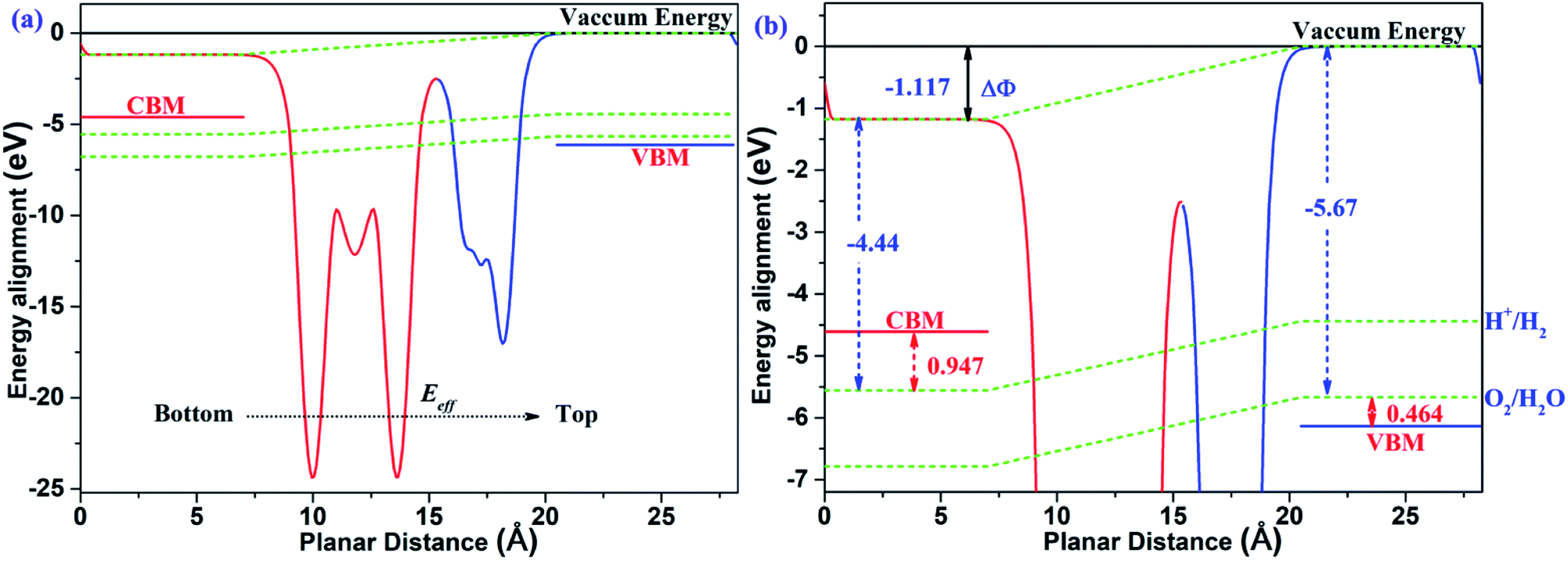
The two-dimensional polarized materials manifest promising and potential properties in the conversion process of solar energy to hydrogen energy, thanks to the effect of the vertical intrinsic electric field. Not only can the carriers be separated efficiently from the interior to the surface under the effect of the intrinsic electric field, but the bandgap is also effectively reduced to align with the redox potential of water, as required for photocatalytic water splitting. According to the mechanism of photocatalytic water splitting by two-dimensional polarized materials introduced by Yang's group,26 under the effect of the intrinsic electric field, all the energies, including vacuum energy, reduction potential and oxidation potential, bend along the direction of the electric field. Therefore, the energy alignment of two-dimensional polarized materials is different from that of non-polarized 2D materials.
As shown in Fig. 7, the MoTe2/GeS vdW heterojunction possesses an intrinsic electric field, which is a combination of the dipole-induced electric field and the interface-induced electric field at the heterojunction. The intrinsic electric field is along the Z direction, therefore the energy, including the vacuum energy, the reduction potential and the oxidation potential, bends along the direction of the electric field. It is obvious that the surface potential difference ΔΦ = 1.177 eV is very helpful to separate the photo-general carriers from the interior to the surface efficiently. Under the effect of the intrinsic electric field, the electrons quickly migrate to the bottom layer of the heterojunction, while the holes migrate to the top layer of the heterojunction. At the top layer of the heterojunction, the VBM energy level is lower than the oxidation potential of O2/H2O (−5.67 eV). The energy difference (ΔEv) between the oxidation potential and the VBM energy level is 0.464 eV, which drives water to generate oxygen and H+ under the action of holes according to the following equation.
| | |
4h+ + 2H2O → O2 + 4H+
| (12) |
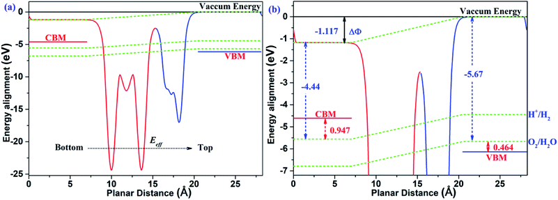 |
| | Fig. 7 (a) The energy alignment of the MoTe2/GeS vdW heterojunction; (b) an enlarged section of (a). | |
In contrast, at the bottom layer of the heterojunction, the CBM energy level is higher compared with the reduction potential of H+/H2 (−4.44 eV). The energy difference (ΔEc) between the reduction potential and the CBM energy level is 0.947 eV, driving water to generate hydrogen and OH− under the action of electrons according to the following equation.
| | |
4e− + 4H2O → 2H2 + 4OH−
| (13) |
Moreover, both ΔEv and ΔEc are suitable for the harmonious reaction. These results indicate that the heterojunction would be a potential and effective photocatalyst for producing hydrogen and oxygen due to the advantages of the intrinsic electric field.
3.5 Optical properties
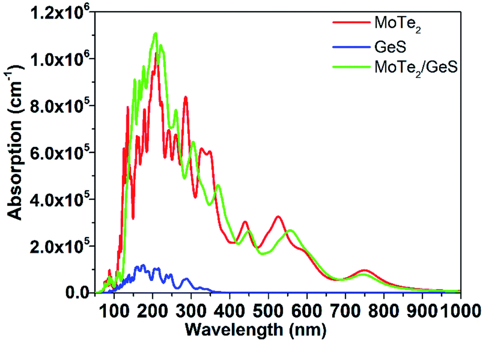
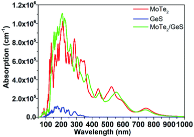
It is known that solar-light absorption is the first and the most important step during the process of solar energy to hydrogen energy conversion. In order to study the absorption performance of the MoTe2/GeS vdW heterojunction, the dielectric function was calculated to obtain the absorption spectrum.69–71 The absorption spectra of the GeS monolayer, MoTe2 monolayer and MoTe2/GeS vdW heterojunction are shown in Fig. 8. It was obvious that the absorption performance of the GeS monolayer was unsatisfactory, involving only the ultraviolet region, which is just about 5% of the solar spectrum. Meanwhile, the visible and infrared regions, which form the most part (about 95%) of the solar spectrum, would not be absorbed efficiently because the bandgap of the GeS monolayer was larger than 3.0 eV. In contrast, the MoTe2 monolayer possessed excellent and distinguishable absorption performance as the MoTe2 monolayer was a direct semiconductor with a suitable bandgap to aid the absorption of a wider range of solar light, including the ultraviolet region (<400 nm) and the visible region (400–800 nm). Moreover, the MoTe2 monolayer had a strong light-absorption capacity, and its absorption coefficient could reach 106 cm−1. The absorption performance of the MoTe2/GeS vdW heterojunction was better than the GeS monolayer as it was mainly determined by the MoTe2 monolayer. Both the ultraviolet spectrum region (<400 nm) and the visible spectrum region (400–800 nm) were absorbed by the MoTe2/GeS vdW heterojunction. Moreover, the absorption coefficient of the MoTe2/GeS vdW heterojunction was about 106 cm−1, indicating excellent and distinguished absorption performance as that of the MoTe2 monolayer. Therefore, the construction of the MoTe2/GeS vdW heterojunction was helpful toward enhancing the conversion efficiency of solar energy and improving the efficiency of photocatalytic water splitting under a wide light spectrum.
 |
| | Fig. 8 Absorption coefficients of the GeS monolayer, MoTe2 monolayer, and MoTe2/GeS vdW heterojunction. | |
4. Conclusion
In summary, we have constructed a MoTe2/GeS vdW heterojunction based on two-dimensional polarized materials and systematically investigated the coupling effect of the dipole-induced electric field and interface-induced electric field on the photocatalytic activity via first-principles calculations. The results indicate that a dipole-induced electric field, which is induced by the GeS monolayer, and an interface-induced electric field, which is induced by the interface between the GeS monolayer and the MoTe2 monolayer, emerge in the 2D polarized MoTe2/GeS vdW heterojunction. The total intrinsic electric field was composed of the dipole-induced electric field and the interface-induced electric field. The dipole-induced electric field was much larger compared to the interface-induced electric field, indicating the dominant contribution of the former to the total intrinsic electric field. Moreover, our results indicate that the two-dimensional polarized MoTe2/GeS vdW heterojunction is a potential efficient photocatalyst for producing hydrogen energy due to the following reasons. The MoTe2/GeS vdW heterojunction is a direct semiconductor with a bandgap of about 1.524 eV, which is very useful for optoelectronic and photocatalytic applications. Moreover, the MoTe2/GeS vdW heterojunction possesses excellent solar absorption performance in a wide light spectrum and presents a high absorption coefficient (about 106 cm−1). The MoTe2/GeS vdW heterojunction possesses a total intrinsic electric field, which is the combination of the dipole-induced electric field and the interface-induced electric field. The intrinsic electric field is helpful in effectively reducing the recombination rate of the electron–hole pairs. The band alignments of the MoTe2/GeS vdW heterojunction satisfy the redox potential very well. On the whole, the two-dimensional polarized material-based MoTe2/GeS vdW heterojunction would be a highly efficient photocatalyst for producing hydrogen energy under ultraviolet to near-infrared light. Our study may shed light on a strategy for building highly efficient 2D polarized vdW heterojunctions for water splitting under the full solar light spectrum.
Data availability
The data that support the findings of this study are available from the corresponding author upon reasonable request.
Author contributions
Di Gu: data curation, formal analysis, conceptualization, investigation, validation, visualization, writing – original draft. Xiaoma Tao: data curation, methodology. Hongmei Chen: visualization, conceptualization. Yifang Ouyang: funding acquisition, project administration, supervision, writing – review & editing. Weiling Zhu: software, supervision, validation, resources. Yong Du: conceptualization.
Conflicts of interest
The authors declare that they have no known competing financial interests or personal relationships that could have appeared to influence the work reported in this paper.
Acknowledgements
Authors acknowledge the financial support from National Natural Science Foundation of China (11964003), Projects of PhDs' Start-up Research of GDUPT (2020bs008) and the Guangxi Natural Science Foundation (2018GXNSFAA281291, 2019GXNSFAA185058).
References
- W. Lubitz and W. Tumas, Chem. Rev., 2007, 107, 3900–3903 CrossRef CAS PubMed.
- P. Kumar, R. Boukherroub and K. Shankar, J. Mater. Chem. A, 2018, 6, 12876–12931 RSC.
- A. J. Esswein and D. G. Nocera, Chem. Rev., 2007, 107, 4022–4047 CrossRef CAS PubMed.
- T. m. Su, Z. z. Qin, H. b. Ji and Z. Wu, Nanotechnology, 2019, 30, 502002 CrossRef CAS PubMed.
- M. Ni, M. K. H. Leung, D. Y. C. Leung and K. Sumathy, Renewable Sustainable Energy Rev., 2007, 11, 401–425 CrossRef CAS.
- J. Ran, J. Zhang, J. Yu, M. Jaroniec and S. Z. Qiao, Chem. Soc. Rev., 2014, 43, 7787–7812 RSC.
- C. Acar, I. Dincer and G. F. Naterer, Int. J. Energy Res., 2016, 40, 1449–1473 CrossRef CAS.
- Y. g. Li, Y. L. Li, B. s. Sa and R. Ahuja, Catal. Sci. Technol., 2017, 7, 545–559 RSC.
- K. Zhang and L. Guo, Catal. Sci. Technol., 2013, 3, 1672 RSC.
- K. M. Lee, C. W. Lai, K. S. Ngai and J. C. Juan, Water Res., 2016, 88, 428–448 CrossRef CAS PubMed.
- N. Xiao, S. Li, X. Li, L. Ge, Y. Gao and N. Li, Chin. J. Catal., 2020, 41, 642–671 CrossRef CAS.
- A. Fujishima and K. Honda, Nature, 1972, 238, 37–38 CrossRef CAS PubMed.
- R. Asahi, T. Morikawa, T. Ohwaki, K. Aoki and Y. Taga, Science, 2001, 293, 269–271 CrossRef CAS PubMed.
- W. Choi, A. Termin and M. R. Hoffmann, J. Phys. Chem., 1994, 98, 13669–13679 CrossRef.
- U. Diebold, Surf. Sci. Rep., 2003, 48, 53–229 CrossRef CAS.
- T. Maric, M. Z. M. Nasir, R. D. Webster and M. Pumera, Adv. Funct. Mater., 2020, 30, 1908614 CrossRef CAS.
- H. G. Yang, C. H. Sun, S. Z. Qiao, J. Zou, G. Liu, S. C. Smith, H. M. Cheng and G. Q. Lu, Nature, 2008, 453, 638–641 CrossRef CAS PubMed.
- T. K. Townsend, N. D. Browning and F. E. Osterloh, ACS Nano, 2012, 6, 7420–7426 CrossRef CAS PubMed.
- K. Domen, A. Kudo and T. Onishi, J. Catal., 1986, 102, 92–98 CrossRef CAS.
- K. Domen, S. Naito, T. Onishi and K. Tamaru, Chem. Phys. Lett., 1982, 92, 433–434 CrossRef CAS.
- H. z. Luo, Z. t. Zeng, G. m. Zeng, C. Zhang, R. Xiao, D. Huang, C. Lai, M. Cheng, W. Wang, W. Xiong, Y. Yang, L. Qin, C. Zhou, H. Wang, Y. Zhou and S. Tian, Chem. Eng. J., 2020, 383, 123196 CrossRef CAS.
- J. b. Pan, S. Shen, W. Zhou, J. Tang, H. z. Ding, J. b. Wang, L. Chen, C.-T. Au and S.-F. Yin, Acta Phys.-Chim. Sin., 2020, 36, 1905068 Search PubMed.
- M. Xiao, B. Luo, Z. Wang, S. Wang and L. Wang, Sol. RRL, 2020, 4, 1900509 CrossRef CAS.
- J. Liu, Y. Liu, N. Y. Liu, Y. Han, X. Zhang, H. Huang, Y. Lifshitz, S. T. Lee, J. Zhong and Z. Kang, Science, 2015, 347, 970–974 CrossRef CAS PubMed.
- C. F. Fu, X. Wu and J. Yang, Adv. Mater., 2018, 30, 1802106 CrossRef PubMed.
- X. X. Li, Z. Y. Li and J. L. Yang, Phys. Rev. Lett., 2014, 112, 018301 CrossRef PubMed.
- Y. Ji, M. Yang, H. Dong, T. Hou, L. Wang and Y. Li, Nanoscale, 2017, 9, 8608–8615 RSC.
- C. F. Fu, X. x. Li, Q. q. Luo and J. Yang, J. Mater. Chem. A, 2017, 5, 24972–24980 RSC.
- J. Yun, Y. Zhang, Y. Ren, P. Kang, J. Yan, W. Zhao, Z. Zhang and H. Guo, Sol. Energy Mater. Sol. Cells, 2020, 210, 110516 CrossRef CAS.
- P. T. Huong, M. Idrees, B. Amin, N. N. Hieu, H. V. Phuc, L. T. Hoa and C. V. Nguyen, RSC Adv., 2020, 10, 24127–24133 RSC.
- C. x. Xia, W. q. Xiong, J. Du, T. Wang, Y. Peng and J. Li, Phys. Rev. B: Condens. Matter Mater. Phys., 2018, 98, 165424 CrossRef CAS.
- Y. Li, J. J. Wang, B. Z. Zhou, F. Wang, Y. Miao, J. Wei, B. Zhang and K. Zhang, Phys. Chem. Chem. Phys., 2018, 20, 24109–24116 RSC.
- A. C. RiisJensen, M. Pandey and K. S. Thygesen, J. Phys. Chem. C, 2018, 122, 24520–24526 CrossRef CAS.
- Y. j. Ji, M. y. Yang, H. p. Lin, T. Hou, L. Wang, Y. Li and S.-T. Lee, J. Phys. Chem. C, 2018, 122, 3123–3129 CrossRef CAS.
- R. Peng, Y. d. Ma, B. b. Huang and Y. Dai, J. Mater. Chem. A, 2019, 7, 603–610 RSC.
- X. c. Ma, X. Wu, H. d. Wang and Y. Wang, J. Mater. Chem. A, 2018, 6, 2295–2301 RSC.
- Y.-L. Liu, Y. Shi, H. Yin and C.-L. Yang, Appl. Phys. Lett., 2020, 117, 063901 CrossRef CAS.
- C. f. Fu, J. y. Sun, Q. q. Luo, X. Li, W. Hu and J. Yang, Nano Lett., 2018, 18, 6312–6317 CrossRef CAS PubMed.
- D. Gu, X. m. Tao, H. m. Chen, W. l. Zhu, Y. Ouyang and Q. Peng, Nanoscale, 2019, 11, 2335–2342 RSC.
- Z. Li, L. Zhang, Y. Liu, C. Shao, Y. Gao, F. Fan, J. Wang, J. Li, J. Yan, R. Li and C. Li, Angew. Chem., 2019, 132, 945–952 CrossRef.
- D. Yu, Z. Liu, J. Zhang, S. Li, Z. Zhao, L. Zhu, W. Liu, Y. Lin, H. Liu and Z. Zhang, Nano Energy, 2019, 58, 695–705 CrossRef CAS.
- D. Gu, X. Tao, H. Chen, Y. Ouyang, W. Zhu, Q. Peng and Y. Du, Phys. Status Solidi RRL, 2019, 13, 1800659 CrossRef.
- B. J. Wang, X. H. Li, R. q. Zhao, X. Cai, W. Yu, W. Li, Z. Liu, L. Zhang and S. Ke, J. Mater. Chem. A, 2018, 6, 8923–8929 RSC.
- S. Wang, C. D. Ren, H. Y. Tian, J. Yu and M. Sun, Phys. Chem. Chem. Phys., 2018, 20, 13394–13399 RSC.
- Y. J. Yuan, Z. j. Li, S. t. Wu, D. Chen, L. Yang, D. Cao, W. Tu, Z. Yu and Z. Zou, Chem. Eng. J., 2018, 350, 335–343 CrossRef CAS.
- R. q. Zhang, L. l. Zhang, Q. j. Zheng, P. Gao, J. Zhao and J. Yang, J. Phys. Chem. Lett., 2018, 9, 5419–5424 CrossRef CAS PubMed.
- Z. f. Zhang, Q. k. Qian, B. k. Li and K. J. Chen, ACS Appl. Mater. Interfaces, 2018, 10, 17419 CrossRef CAS PubMed.
- C. F. Fu, R. Zhang, Q. Luo, X. Li and J. Yang, J. Comput. Chem., 2019, 40, 980–987 CrossRef CAS PubMed.
- R. Kumar, D. Das and A. K. Singh, J. Catal., 2018, 359, 143–150 CrossRef CAS.
- Y. Liang, J. W. Li, H. Jin, B. Huang and Y. Dai, J. Phys. Chem. Lett., 2018, 9, 2797–2802 CrossRef CAS PubMed.
- C. Long, Y. Dai, Z. R. Gong and H. Jin, Phys. Rev. B: Condens. Matter Mater. Phys., 2019, 99, 115316 CrossRef CAS.
- W. j. Yin, B. Wen, Q. x. Ge, D. Zou, Y. Xu, M. Liu, X. Wei, M. Chen and X. Fan, Prog. Nat. Sci.: Mater. Int., 2019, 29, 335–340 CrossRef CAS.
- J. Zhang, X. b. Chen, Y. Bai, C. Li, Y. Gao, R. Li and C. Li, J. Mater. Chem. A, 2019, 7, 10264–10272 RSC.
- Z. Liu, X. Yu and L. Li, Chin. J. Catal., 2020, 41, 534–549 CrossRef CAS.
- D. Ren, R. Shen, Z. Jiang, X. Lu and X. Li, Chin. J. Catal., 2020, 41, 31–40 CrossRef CAS.
- S. Shenoy and K. Tarafder, J. Phys.: Condens. Matter, 2020, 32, 275501 CrossRef CAS PubMed.
- Y. J. Yuan, Z. k. Shen, S. t. Wu, Y. b. Su, L. Pei, Z. Ji, M. Ding, W. Bai, Y. Chen, Z. Yu and Z. Zou, Appl. Catal., B, 2019, 246, 120–128 CrossRef CAS.
- Y. J. Yuan, P. Wang, Z. j. Li, Y. z. Wu, W. Bai, Y. Su, J. Guan, S. Wu, J. Zhong, Z. Yu and Z. Zou, Appl. Catal., B, 2019, 242, 1–8 CrossRef CAS.
- Z. w. Li, J. g. Hou, B. Zhang, S. Cao, Y. Wu, Z. Gao, X. Nie and L. Sun, Nano Energy, 2019, 59, 537–544 CrossRef CAS.
- D. Gu, X. m. Tao, H. m. Chen, W. l. Zhu, Y. Ouyang, Y. Du and Q. Peng, Phys. Status Solidi RRL, 2019, 14, 1900582 CrossRef.
- Y. Zhao, Y. He, M. Zhang and J. Shi, J. Inorg. Mater., 2020, 35, 993–998 CrossRef.
- G. Kresse and J. Furthmüller, Phys. Rev. B: Condens. Matter Mater. Phys., 1996, 54, 11169–11186 CrossRef CAS PubMed.
- J. P. Perdew, K. Burke and M. Ernzerhof, Phys. Rev. Lett., 1996, 77, 3865–3868 CrossRef CAS PubMed.
- P. E. Blochl, Phys. Rev. B: Condens. Matter Mater. Phys., 1994, 50, 17953–17979 CrossRef PubMed.
- A. D. Becke, Phys. Rev. A: At., Mol., Opt. Phys., 1988, 38, 3098–3100 CrossRef CAS PubMed.
- J. Klimeš, D. R. Bowler and A. Michaelides, J. Phys.: Condens. Matter, 2009, 22, 022201 CrossRef PubMed.
- J. Paier, M. Marsman, K. Hummer, G. Kresse, I. C. Gerber and J. G. Angyan, J. Chem. Phys., 2006, 124, 154709 CrossRef CAS PubMed.
- H. J. Monkhorst and J. D. Pack, Phys. Rev. B: Solid State, 1976, 13, 5188–5192 CrossRef.
- Q. Peng, Z. Y. Wang, B. S. Sa, B. Wu and Z. Sun, Sci. Rep., 2016, 6, 31994 CrossRef CAS PubMed.
- C. x. Xia, J. Du, X. w. Huang, W. Xiao, W. Xiong, T. Wang, Z. Wei, Y. Jia, J. Shi and J. Li, Phys. Rev. B: Condens. Matter Mater. Phys., 2018, 97, 115416 CrossRef CAS.
- W. Zhang and L. f. Zhang, RSC Adv., 2017, 7, 34584–34590 RSC.
- Y. Ding, Y. l. Wang, J. Ni, L. Shi, S. Shi and W. Tang, Phys. B, 2011, 406, 2254–2260 CrossRef CAS.
- T. Hu and J. M. Dong, Phys. Chem. Chem. Phys., 2016, 18, 32514–32520 RSC.
- Y. Qun, C. j. Tan, R. s. Meng, J. Junke, L. Qiuhua, S. Xiang, Y. Daoguo and C. Xianping, IEEE Electron Device Lett., 2017, 38, 145–148 Search PubMed.
- B. J. Wang, X. H. Li, X. L. Cai, W. Yu, L. Zhang, R. Zhao and S. Ke, J. Phys. Chem. C, 2018, 122, 7075–7080 CrossRef CAS.
- C. x. Xia, J. Du, W. q. Xiong, Y. Jia, Z. Wei and J. Li, J. Mater. Chem. A, 2017, 5, 13400–13410 RSC.
- L. Fang, Q. Feng and S. N. Luo, J. Phys.: Condens. Matter, 2019, 31, 405705 CrossRef CAS PubMed.
- A. Kormányos, G. Burkard, M. Gmitra, J. Fabian, V. Zólyomi, N. D. Drummond and V. Fal'ko, 2D Materials, 2015, 2, 022001 CrossRef.
Footnote |
| † Electronic supplementary information (ESI) available. See DOI: 10.1039/d1ra05840a |
|
| This journal is © The Royal Society of Chemistry 2021 |
Click here to see how this site uses Cookies. View our privacy policy here. 
 Open Access Article
 This Open Access Article is licensed under a Creative Commons Attribution-Non Commercial 3.0 Unported Licence
 *b,
Weiling Zhu*a and
Yong Duc
*b,
Weiling Zhu*a and
Yong Duc