DOI:
10.1039/D1RA05639E
(Paper)
RSC Adv., 2021,
11, 35614-35623
Tuning MoSO monolayer properties for optoelectronic and spintronic applications: effect of external strain, vacancies and doping†
Received
23rd July 2021
, Accepted 29th October 2021
First published on 3rd November 2021
Abstract
Since the successful synthesis of the MoSSe monolayer, two-dimensional (2D) Janus materials have attracted huge attention from researchers. In this work, the MoSO monolayer with tunable electronic and magnetic properties is comprehensively investigated using first-principles calculations based on density functional theory (DFT). The pristine MoSO single layer is an indirect gap semiconductor with energy gap of 1.02(1.64) eV as predicted by the PBE(HSE06) functional. This gap feature can be efficiently modified by applying external strain presenting a decrease in its value upon switching the strain from compressive to tensile. In addition, the effects of vacancies and doping at Mo, S, and O sites on the electronic structure and magnetic properties are examined. Results reveal that Mo vacancies, and Al and Ga doping yield magnetic semiconductor 2D materials, where both spin states are semiconductors with significant spin-polarization at the vicinity of the Fermi level. In contrast, single S and O vacancies induce a considerable gap reduction of 52.89% and 58.78%, respectively. Doping the MoSO single layer with F and Cl at both S and O sites will form half-metallic 2D materials, whose band structures are generated by a metallic spin-up state and direct gap semiconductor spin-down state. Consequently, MoV, MoAl, MoGa, SF, SCl, OF, and OCl are magnetic systems, and the magnetism is produced mainly by the Mo transition metal that exhibits either ferromagnetic or antiferromagnetic coupling. Our work may suggest the MoSO Janus monolayer as a prospective candidate for optoelectronic applications, as well as proposing an efficient approach to functionalize it to be employed in optoelectronic and spintronic devices.
I. Introduction
Pushed by the success of graphene,1–3 the investigation of two-dimensional (2D) materials at atomic thickness has been continuously increased experimentally and theoretically. Between the materials studied so far, it would be wrong not to mention the transition metal dichalcogenides (TMDs).4,5 Being an important member of the TMD family, the MoS2 monolayer has been extensively investigated. Previously, Yu et al.6 have successfully prepared large-area and high quality MoS2 monolayers and few-layer films using a self-limiting approach, which made possible the fabrication of miniature devices. Large-area synthesis at 200 °C of the high phase purity and crystallinity MoS2 monolayer has been achieved by Gong et al.7 using chemical vapour deposition (CVD). The synthesized single layer shows significant fluorescence, however the intensity decreases considerably according to the increase in layer number as a result of the direct–indirect gap transition. It has been demonstrated that the photoluminescence yield of the MoS2 monolayer can reach high values close to 100% using superacid treatment.8,9 Liu et al.10 have shown that the 2D hybrid materials based on the monolayer MoS2 films are promising photodetectors exhibiting high responsivity near 1.8 ×10⁴ A W−1 and ultrahigh detectivity near 7.6 ×10¹³ Jones. The MoS2 monolayer has been also suggested as an excellent 2D electrocatalyst for application in the hydrogen evolution reaction (HER), showing a Tafel slope of 61 mV per decade and exchange current density of 38.1 μA cm−2.11 Theoretically, first-principles calculations carried out by Yelgel et al.12 yield a direct energy gap of 1.85 eV for the MoS2 single layer. Besides, the modulation of the fundamental properties of the MoS2 monolayer has been also investigated using different methods such as application of external strain,13,14 formation of intrinsic defects,15,16 and doping,17,18 which are efficient in inducing novel properties in the layer.
On the other hand, a new 2D materials family called “Janus” has been developed from 2017 with the successful synthesis of the MoSSe monolayer, which is formed by breaking the out-of-plane mirror symmetry. This is achieved by either replacing the S top-layer in MoS2 monolayer with Se atoms19 or Se-layer in MoSe2 monolayer with S atoms using a controlled sulfurization approach.20 Later, Roberto et al.21 have carried out the sulfurization of the PtSe2 single layer on Pt(111) substrate under H2S atmosphere. Chemical composition analysis has demonstrated the Se-by-S substitution in the topmost layer, indicating the formation of PtSSe Janus monolayer. Theoretically, many 2D TMD Janus materials with good stability and novel properties have been predicted.22,23 However, studies have not been only limited to TMDs, but the chemical composition has been extended to other possible combinations. For examples, IIIA-group chalcogenides Janus monolayers have been investigated. Results indicate prospect of their electronic, optical, and piezoelectric properties.24–27 Semiconductor layered BiTeCl and BiTelBr compounds with giant Rashba-splitting have been prepared by Debarati et al.28 Theoretical calculations yield small energy gaps of 0.83 and 0.80 eV,29 respectively. Besides, a large variety of Janus single layers based on chalcogens and halogens with feature-rich properties have been reported in the computational 2D materials database (C2DB).30,31 Janus Ga2XO structures (X = S, Se, Te) have been designed by Demirtas et al.32 using first-principles calculations. Results indicate good dynamical and mechanical stability of Ga2SO and Ga2SeO. These possess direct band-gap that can be further tuned by external strain. Demirtas et al.33 have also predicted the Al2XX′ (X/X′ = O, S, Se, and Te) with energy gap ranging from 1.07 to 2.74 eV, using first-principles method. Janus In2XO (X = S, Se, and Te) as potential nanomaterials for applications in optoelectronic and thermal devices have been studied by Vu et al.34 In a recent work, we have investigated the PtOX (X = S and Se) monolayers,35 results indicate prospective optoelectronic and thermoelectric features of these 2D materials.
The oxidation of MoS2 monolayer to form intermediate phase composed of MoSxOy has been realized by Xu et al.36 through hydrogen peroxide (H2O2) treatment. Photoluminescence spectra show an effective band gap modulation induced by the oxidation. Yagmurcukardes et al.37 have investigated the MoSO single layer electronic and photonic properties under biaxial strain. A strong out-of-plane piezoelectricity and indirect gap semiconductor are characterized, where the energy gap can be effectively engineered. Using MoSO monolayer as a building block, the Janus-MoSO/MoS2 heterojunction has been investigated by Wang et al.38 Results show an improvement of the optoelectronic performance of the structure based on MoSO monolayer. In this work, we explore the structural, electronic, and magnetic properties of the MoSO Janus monolayer using first-principles calculations. As a first step, the structure is optimized, followed by the test of dynamical and thermal stability. Then, the electronic properties are studied analyzing the band structure, density of states, and charge density difference. In addition, the effect of external strain, vacancies, and doping at different sites of MoSO single layer will be considered in order to induce novel electronic and magnetic properties. Hereafter, the MoV, MoAl, and MoGa terms refer to the MoSO monolayer with a single Mo vacancy, Al doping at Mo site, and Ga doping at Mo site, respectively. Similarly, the structures with a single S(O) vacancy, doped with F, and doped with Cl at S(O) site will be denoted by SV(OV), SF(OF), and SCl(OCl), respectively.
II. Computational details
First-principles calculations in framework of the density functional theory (DFT)39 have been performed using CASTEP computational package40 to explore the structural, electronic, and magnetic properties of MoSO Janus monolayer under effect of external strain, vacancy, and doping. The generalized gradient approximation in Perdew–Burke–Ernzerhof form (GGA-PBE)41 is included in calculation to take into account the effect of exchange-correlation potentials, while the norm-conserving pseudopotential describes the electron-ion interactions. The expansion of plane waves is truncated with a kinetic energy cut-off of 500 eV. The Brillouin zone sampling is done with a k-mesh of 20 × 20 × 1 and 6 × 6 × 1 in the pristine primitive cell and supercell cases, respectively. The structures optimization is realized with a force criterion of 0.01 (eV Å−1). Stopping point for self-consistent iterations is set to 10−6 eV. In all calculations, a vacuum gap of width 15 (Å) is generated along the direction perpendicular to the layer plane, which is large enough to exclude the interactions of periodic layers.
III. Results and discussion
A. Pristine MoSO monolayer
It is well known that MoS2 can be found in either 1T or 2H phases, where the later is more common and is considered in this work. Similar to the MoSSe Janus monolayer, the MoSO structure is generated by substituting completely one of the two S-layers by O atoms. This fact breaks the structural mirror-symmetry, reducing the symmetry to P3m1 space group (no. 156) (see Fig. 1a). According to our calculations, the optimized lattice parameter is 3.05 (Å), which is smaller than that of MoS2,42 as a result of the smaller atomic size of O atom as compared to S atom. The calculated bond lengths are dMo–S = 2.41 and dMo–O = 2.13, and interatomic angle ∠SMoO = 77.33°. In addition, a total thickness of 2.84 (Å) is generated by the buckling heights ΔMo–S and ΔMo–O of 1.64 (Å) and 1.20 (Å), respectively. Following the structural optimization, the dynamical and thermal stability of the predicted single layer is examined. Fig. 1b shows the phonon dispersion curves, which are formed by nine phonon modes resulting from the vibrations of three constituent atoms in the primitive cell. From the figure it can be noted no imaginary vibrational frequency, that is all phonon modes are positive, indicating that MoSO Janus single layer is dynamically stable. Further ab-initio molecular dynamics (AIMD) simulations have been carried out, results are displayed in Fig. 1c and d. The recorded snapshots suggest that no structural destruction occurs at room temperature (300 K) and high temperature (1000 K), confirming good structural-thermal stability of the considered pristine Janus monolayer. In addition, we have calculated the formation enthalpy ΔHf using following formula:| |
 | (1) |
where Et denotes the total energy; μ refers to the chemical potential of each element in the parentheses. Our calculations yield a negative ΔHf of −1.24 (eV per atom), suggesting a good thermodynamic stability of MoSO Janus single layer.31 As a stable 2D Janus structure, the intrinsic strain induced by the large difference in atomic size of S and O atoms may favor rolling the MoSO flakes into a nanotube with unique electronic properties.43–45 Therefore, our results may stimulate future works treating about new MoSO nanotubes.
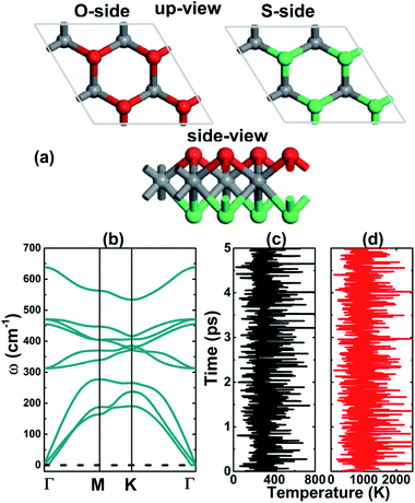 |
| | Fig. 1 (a) Atomic structure (gray ball: Mo; red ball: O; green ball: S), (b) phonon dispersion curves, and fluctuation of temperature as a function of molecular dynamics simulation steps of MoSO monolayer at (c) 300 K and (d) 1000 K. | |
The electronic band structure of MoSO single layer has been calculated within the PBE and HSE06 formalism. Fig. 2a shows results depicted along the Γ–M–K–Γ high symmetry direction. Note that the indirect gap semiconductor nature is predicted by both employed functionals, since the valence band maximum takes place at Γ point and the conduction band minimum occurs at K point. Previous studies have indicated the K–K,42 and the direct–indirect gap transition may be induced with the formation of Janus structure as a result of the anisotropic strains experienced by opposite O-side and S-side. At equilibrium, the energy gap of the pristine monolayer is 1.02 eV as obtained by PBE. Undoubted that with the introduction of 25% exact Hartree–Fock exchange potential, the hybrid functional HSE06 improves considerably the results of standard GGA potentials, giving more accurate energy gap of materials. In our case, the HSE06 yields a band gap value of 1.64 eV, which is 60.75% larger than that determined by PBE functional. Choosing the MoS2 monolayer as a reference, it can be seen that this important parameter reduces according to the decrease in atomic number of VI-A group elements, similar to other Janus based on TMDs46 and III-A chalcogenides.33 To get deeper understanding on the band structure formation, the partial density of states (PDOS) is studied. Fig. 2b shows that the Mo-4d, S-3p, and O-2p are main contributors, exhibiting significant presence in both valence band and conduction band. A closer analysis indicates that the non-metal atoms have higher influence in the valence band, and the same behavior is observed for the transition metal in the conduction band. In addition, the charge density difference is investigated to examine the chemical bonds. Results illustrated in Fig. 2c indicate that the charge is accumulated at O- and S-sites, while the charge depletion is observed at the Mo-site, indicating a charge transfer from Mo atom to O and S atoms, suggesting an ionic chemical bond. According to our calculations, O and S atoms gain a charge quantity of 0.58 and 0.04e, respectively, in agreement with the considerably larger electronegativity of O atom.
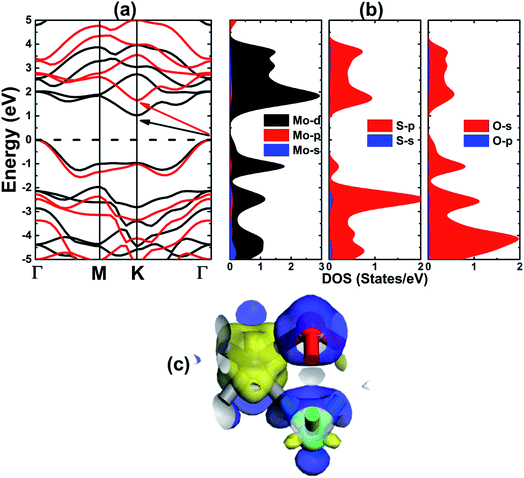 |
| | Fig. 2 (a) Electronic band structure (black line PBE; red line: HSE06), (b) partial density of states, and (c) charge density difference (blue surface: charge accumulation; yellow surface: charge depletion) of the MoSO monolayer. | |
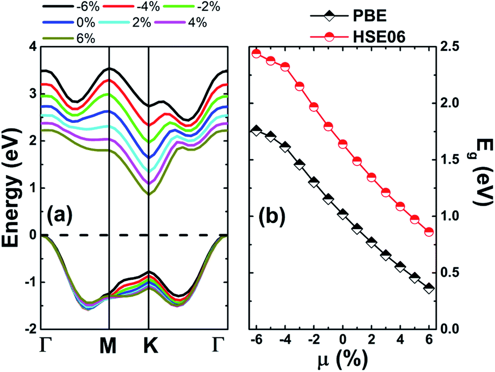
Since one of the most frequent factors that influence the fundamental properties of 2D materials is the external strain, which may be generated by the hydrostatic pressure or chemical pressure. Therefore, to achieve an adequate design of these materials, a complete understanding on this dependence should not be forgotten. Herein, we investigate the strain effect on the electronic properties of the MoSO monolayer, which is defined by the strain lattice parameter a and equilibrium lattice parameter a0 as follows: 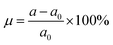 . Results of the band structure and energy gaps are given in Fig. 3. From the left panel, one can see that in the considered energy range from −6% to 6%, this Janus monolayer retains its indirect gap semiconductor nature considering that the VBM and CBM are located at Γ and K point at a given strain, respectively. The band gap plots in the right panel indicate that this parameter decreases considerably when switching the strain nature from compressive to tensile. Note that the reduction rate is considerably smaller in the strain range from −6% to −4%, from which a nearly linear decreasing trend is obtained. MoSO monolayer exhibits an increase of 72.52(48.90)% up to a compressive strain strength of −6% as predicted by PBE(HSE6) potential, while a reduction of the order of −55.25(−40.66)% when the lattice tension of 6% is applied.
 |
| | Fig. 3 (a) Electronic band structure and (b) energy gap values of the MoSO monolayer at several strains. | |
B. Vacancy and doping at Mo site
Because of the atomic size difference and modification of electronic interactions, the formation of vacancy and doping induce local changes in the structure (see the relaxed atomic structures displayed in Fig. S1†), which are summarized in Table 1. Note that in the case of MoV system, the structural parameters exhibit quite small difference as compared with those of the pristine layer, suggesting that the Mo vacancy effect on the structure is negligible. In contrast, significant structural re-arrangements are noted for the cases of Al and Ga doping. Specifically, in comparison with the pristine monolayer both dD–S and dD–O bonds lengths increase. A same behavior is noted for the buckling height ΔD–S, while ΔD–O and interatomic angles show a decreasing variation. It is worth mentioning that the Al doping may induce stronger structural modification than Ga doping, where Al dopant is nearly found in the O-layer plane showing a buckle of only 0.07 (Å). These results suggest a stronger Al–O bond than Ga–O one.
Table 1 Bond length d (Å), buckling height Δ (Å), interatomic angle ∠ (°), formation energy Ef (meV Å−2) and cohesive energy Ec (eV per atom) of the MoSO monolayer with defect at Mo-site (D = Mo in MoV system; D = Al in MoAl system; D = Ga in MoGa system)
| |
dD–S |
dD–O |
ΔD–S |
ΔD–O |
∠SDO |
Ef |
Ec |
| MoV |
2.40 |
2.02 |
1.66 |
1.19 |
79.80 |
74 |
−3.92 |
| MoAl |
3.28 |
1.69 |
2.79 |
0.07 |
60.73 |
−4.40 |
−3.86 |
| MoGa |
2.60 |
1.99 |
1.88 |
0.95 |
74.59 |
41 |
−3.71 |
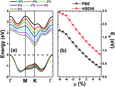
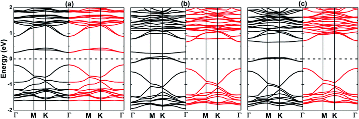
Fig. 4 displays the spin-resolved band structures of the O-vacancy and doped MoSO Janus monolayer. It can be noted novel electronic features generated by the spin-polarization, mostly at vicinity of the Fermi level that is set as an energy reference. In the case of MoV system, the indirect KΓ–M band gaps of 0.28 and 0.48 eV are obtained in the spin-up and spin-down state, respectively. These are generated by the pair [VBM![[thin space (1/6-em)]](https://www.rsc.org/images/entities/char_2009.gif) :CBM] at energies of [−0.14:0.14] eV and [−0.20:0.28] eV, respectively. The substitutional incorporation of Al and Ga at the Mo site gives place to the appearance of a spin-up direct Γ–Γ gap of 0.51 and 0.60 eV, respectively. In the MoAl spin-down configuration, the VBM and CMB are found at Γ point (−0.38 eV) and K point (0.63 eV), respectively, originating an indirect gap of 1.01 eV. The indirect gap semiconductor behavior is also obtained in the MoGa spin-down state with an energy gap of 1.07 eV generated by the separation of the VBM at −0.25 eV (along KΓ direction) and CBM at 0.82 eV (at K point). Results indicate that the creation of Mo vacancy, as well as Al and Ga doping conduct to the formation of 2D magnetic semiconductor materials. It is well known that when the un-polarized electrons pass through a magnetic semiconductor film, the spin states will encounter different potential barriers which influence considerably the probability of tunneling of each of them.47 Therefore, the systems studied herein may be prospectively used as a spin-filter to create the spin currents to be used in the spintronic devices. The band structures of MoV, MoAl, and MoGa systems are formed mainly by the Mo-4d, S-3p, and P-2p states, similar to the pristine layer (see Fig. S4†). In addition, small contribution from the s and p orbitals of dopants is also noted in both valence band and conduction band. The population analysis indicates a significant charge transfer from Mo (a quantity between 0.61 and 0.78e) and dopants (1.62e of Al and 0.48e of Ga) to S and O atoms. Undoubted that most of these charges are transferred to O atom considering its larger electronegativity as compared with that of S atom (see results listed in Table 2).
:CBM] at energies of [−0.14:0.14] eV and [−0.20:0.28] eV, respectively. The substitutional incorporation of Al and Ga at the Mo site gives place to the appearance of a spin-up direct Γ–Γ gap of 0.51 and 0.60 eV, respectively. In the MoAl spin-down configuration, the VBM and CMB are found at Γ point (−0.38 eV) and K point (0.63 eV), respectively, originating an indirect gap of 1.01 eV. The indirect gap semiconductor behavior is also obtained in the MoGa spin-down state with an energy gap of 1.07 eV generated by the separation of the VBM at −0.25 eV (along KΓ direction) and CBM at 0.82 eV (at K point). Results indicate that the creation of Mo vacancy, as well as Al and Ga doping conduct to the formation of 2D magnetic semiconductor materials. It is well known that when the un-polarized electrons pass through a magnetic semiconductor film, the spin states will encounter different potential barriers which influence considerably the probability of tunneling of each of them.47 Therefore, the systems studied herein may be prospectively used as a spin-filter to create the spin currents to be used in the spintronic devices. The band structures of MoV, MoAl, and MoGa systems are formed mainly by the Mo-4d, S-3p, and P-2p states, similar to the pristine layer (see Fig. S4†). In addition, small contribution from the s and p orbitals of dopants is also noted in both valence band and conduction band. The population analysis indicates a significant charge transfer from Mo (a quantity between 0.61 and 0.78e) and dopants (1.62e of Al and 0.48e of Ga) to S and O atoms. Undoubted that most of these charges are transferred to O atom considering its larger electronegativity as compared with that of S atom (see results listed in Table 2).
 |
| | Fig. 4 Spin-polarized band structure (black line: spin-up; red line: spin-down) (a) MoV, (b) MoAl, and (c) MoGa systems. | |
Table 2 Calculated band gap Eg (eV) (M: metal) and electronic nature (MS: magnetic semiconductor; S: semiconductor; HM: half-metallic), ionic charge Q (e), and local magnetic moment M(μB) of the vacancy-defective and doped MoSO Janus monolayer (D = vacancy, Al, Ga, F, or Cl; Mo1, Mo2, and Mo3 denote the Mo atom with increasing distance from vacancy and doping site
| |
Eg |
Q |
M |
| Spin-up |
Spin-down |
Nature |
Mo |
S |
O |
D |
Mo1 |
Mo2 |
Mo3 |
S |
O |
D |
| MoV |
0.28 |
0.48 |
MS |
0.61 ÷ 0.71 |
−0.03 ÷ −0.11 |
−0.51 ÷ −0.60 |
|
0.14 |
−0.20 |
−0.21 |
−0.01 |
0 ÷ −0.02 |
|
| MoAl |
0.51 |
1.01 |
MS |
0.62 ÷ 0.72 |
−0.03 ÷ −0.16 |
−0.58 ÷ −0.86 |
1.62 |
0.64 |
−0.38 |
−0.52 |
−0.03 ÷ 0.13 |
−0.01 ÷ 0.02 |
−0.01 |
| MoGa |
0.60 |
1.07 |
MS |
0.70 ÷ 0.78 |
−0.02 ÷ −0.17 |
−0.58 ÷ −0.65 |
0.48 |
0.74 |
−0.58 |
−0.64 |
−0.08 ÷ 0.03 |
−0.01 ÷ 0.03 |
−0.03 |
| SV |
0.48 |
0.48 |
S |
0.55 ÷ 0.66 |
−0.03 ÷ −0.06 |
−0.57 ÷ −0.58 |
|
0.00 |
0.00 |
0.00 |
0.00 |
0.00 |
|
| SF |
M |
1.04 |
HM |
0.56 ÷ 0.78 |
−0.04 ÷ −0.05 |
−0.57 ÷ −0.58 |
−0.44 |
0.77 |
−0.29 |
−0.07 |
−0.01 ÷ 0.03 |
−0.01 ÷ −0.06 |
0.00 |
| SCl |
M |
1.06 |
HM |
0.62 ÷ 0.65 |
−0.05 |
−0.58 ÷ −0.60 |
−0.11 |
0.73 |
−0.26 |
−0.10 |
−0.01 ÷ −0.03 |
−0.05 ÷ 0.02 |
0.00 |
| OV |
0.42 |
0.42 |
S |
0.40 ÷ 0.68 |
−0.03 ÷ −0.04 |
−0.58 ÷ −0.59 |
|
0.00 |
0.00 |
0.00 |
0.00 |
0.00 |
|
| OF |
M |
2.28 |
HM |
0.58 ÷ 0.65 |
−0.04 |
−0.58 |
−0.45 |
0.42 |
−0.08 |
−0.02 |
−0.06 ÷ 0.01 |
−0.01 ÷ 0.00 |
0.05 |
| OCl |
M |
1.33 |
HM |
0.46 ÷ 0.66 |
−0.03 ÷ −0.05 |
−0.58 ÷ −0.59 |
−0.12 |
0.17 |
0.04 |
0.13 |
−0.03 ÷ −0.05 |
−0.02 ÷ 0.00 |
0.02 |
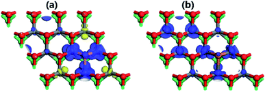
The break of spin symmetry close to the Fermi level may suggest significant magnetization in the MoSO Janus monolayer induced by Mo vacancy, and Al and Ga doping. According to our calculations, the magnetism is induced mainly by the Mo atoms (see Table 2). Specifically, in MoV system the first, second, and third Mo atoms closest to the vacancy exhibit magnetic moments of 0.14, −0.20, and −0.21 μB, respectively. While in the doped systems, larger values of [0.64 and 0.74], [−0.38 and −0.57], and [−0.52 and −0.64] μB are obtained. It is worth mentioning that the first Mo atoms from vacancy and doping site show an antiferromagnetic coupling with the remaining second and third ones provided that their magnetic moments exhibit opposite orientations. This feature is illustrated clearly in the spin density maps (Fig. 5). Such magnetization is originated mainly by the first Mo spin-up, and second and third Mo spin-down states, being in agreement with the numerical results. In all cases, the contribution of S, O, Al, and Ga atoms to the magnetic properties is quite small.
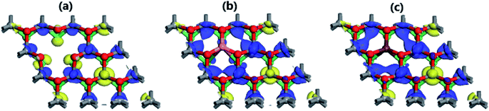 |
| | Fig. 5 Spin density (blue surface: spin-up; yellow surface: spin-down) of (a) MoV (iso-surface of value 0.02), (b) MoAl (iso-surface of value 0.05), and (c) MoGa (iso-surface of value 0.05) systems. | |
C. Vacancy and doping at S site
Now, the effect of single S vacancy, and F and Cl doping at S site on the structural, electronic, and magnetic properties of MoSO monolayer is examined. The optimized atomic structures of the SV, SF, and SCl systems are illustrated in Fig. S2,† and parameters calculated around the vacancy and doping site are given in Table 3. It appears that the S vacancy induces negligible change of the interatomic distances (dMo–S and dMo–O), and angle (∠SMoO), and buckling height ΔMo–O. The most notable modification is that of the layer thickness with an increase of 0.09 (Å) in the buckle ΔMo–S. Results suggest that in terms of the structure, the O-side may not suffer of significant effect of a single S vacancy. Similar behavior is noted in the case of F and Cl doping, where only quite small differences of dMo–O and ΔMo–O in comparison with their corresponding values in the pristine layer are perceived. However, in these two cases, the doping leads to an important local distortion in the S-side. Specifically, the F substitution causes a structural shrink indicated by the reduction of the chemical bond length dMo–S, buckling height ΔMo–S, and angle ∠SMoO. On the contrary, a significant local tension is induced by Cl doping since these mentioned parameters increase after replacing one S atom by one Cl atom.
Table 3 Bond length d (Å), buckling height Δ (Å), interatomic angle ∠ (°), formation energy Ef (meV Å−2) and cohesive energy Ec (eV per atom) of the MoSO monolayer with defect at S-site (D = S in SV system; D = F in SF system; D = Cl in SCl system)
| |
dMo–D |
dMo–O |
ΔMo–D |
ΔMo–O |
∠DMoO |
Ef |
Ec |
| SV |
2.40 |
2.11 |
1.73 |
1.12 |
77.79 |
31 |
−4.37 |
| SF |
2.29 |
2.11 |
1.45 |
1.15 |
72.50 |
−10.60 |
−4.05 |
| SCl |
2.55 |
2.11 |
1.82 |
1.12 |
77.56 |
15.14 |
−3.98 |
Fig. 6 shows the spin-polarized electronic band structure of the SV, SF, and SCl systems in panels a, b, and c, respectively. Note that the creation of single S vacancy in MoSO Janus monolayer leads to the formation of a non-magnetic 2D material since its spin channels exhibit a completely symmetric curves in both valence band and conduction band. Considering the Brillouin zone of the hexagonal defective supercell, SV layer is a Γ–Γ direct gap semiconductor with an energy gap of 0.48 eV (generated by the VBM at 0.23 eV below the Fermi level and the CBM at 0.25 eV above the Fermi level). This result corresponds to a reduction of the order of 52.89% as compared with that of the pristine layer. In contrast, spin-polarized nature is noted around the Fermi energy in the cases of doping. With the similar valence configurations (2s22p5 of F and 3s23p5 of Cl), one can expect similar effect of F and Cl doping on the electronic structure of MoSO Janus single layer. This expectation is met in our case. To precise, the half-metallicity is achieved by the incorporation by substitution of these halogens at S site, which is generated by a metallic spin-up state and a semiconductor spin-down state. In the spin-up channel, the metallic nature is caused by electronic states overlapping the Fermi level. While the direct gap semiconductor behavior in the spin-down channel is a result of the separation between VBM and CBM, both at Γ point. In this later, the obtained spin-down band gap of the SF and SCl layer is 1.04 eV (with VBM at −0.38 eV and CBM at 0.66 eV) and 1.06 eV (VBM at 0.36 eV and CBM at 0.70 eV), which are quite similar to that of the pristine MoSO layer. In recent years, spintronics has been considered as next generation electronics replacing the silicon based conventional electronics. In this regard, creating the spin current is a one of the main tasks. For such a goal, besides the magnetic semiconductors (as seen above), the half-metallic materials are widely employed.48 Therefore, the F and Cl doping at S site may be an efficient method to functionalize the MoSO Janus monolayer for the use in spintronic devices to generate spin current. Further calculations of the PDOS indicate that in the considered energy range, the band structures of the studied nano-structures are formed mainly by the Mo-d, S-p, and O-p states (see Fig. S5†). It is also noted small contribution of the F-p and Cl-p orbitals in the SS and SCl systems, respectively. The PDOS is totally symmetric in the layer with vacancy presence, in agreement with the band structure. Note that the spin-up metallic nature of the doped layers is induced mainly by the Mo-4d state since this exhibits quite high weight at the Fermi level. Analyzing the electronic population, we observe a charge transfer from Mo transition metal to the non-metal constituents including the F and Cl dopants (see details in Table 2). Clearly, greater amount is transferred to the O-side, while with a larger electronegativity the F and Cl atoms gain larger charge than S atoms in the S-side.
 |
| | Fig. 6 Spin-polarized band structure (black line: spin-up; red line: spin-down) of (a) SV, (b) SF, and (c) SCl systems. | |
The electronic structure analysis suggests that the F and Cl doping at the S site, breaking mainly the spin symmetry of Mo-d orbital, have significantly magnetized the MoSO Janus monolayer. Consequently, the magnetic properties are produced mainly by the Mo transition metal (see Table 2). Our simulations yield magnetic moments of 0.77(0.73), −0.29(−0.26), and −0.07(−0.10) μB for the first, second, and third Mo atoms from the F(Cl) doping site, respectively. Note that the contribution of the third ones is quite small, whereas the opposite signs suggest an antiferromagnetic coupling of the first and second atoms in both cases. This result is illustrated via spin density in Fig. 7. The iso-surfaces indicate that the magnetism is induced mainly by the first Mo spin-up state and second Mo spin-down state, being consistent with the numerical results.
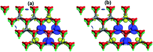 |
| | Fig. 7 Spin density (blue surface: spin-up; yellow surface: spin-down) of (a) SF and (b) SCl (iso-surface of value 0.05) systems. | |
D. Vacancy and doping at O site
In this subsection, we investigate the structural, electronic, and magnetic properties of the MoSO Janus monolayer under effect of a single O vacancy, and F and Cl doping at the O site. The readers can find the optimized atomic structures of these systems in Fig. S3.† Structural parameters are given in Table 2. Similar to the SV structure, creating an O vacancy induces insignificant structure modifications. Similar effect is obtained in the S-side when the layer is doped with F and Cl at O site provided that the bond length and buckling height related to the S atoms exhibit negligible difference in comparison with those in the pristine layer. On the contrary, a considerable atomic re-arrangement takes place at the O-side, causing a local tension since the parameters dMo–F–dMo–Cl, ΔMo–F–ΔMo–Cl, and ∠SMoF–∠SMoCl are larger than their corresponding values related to O atom in the MoSO single layer. Clearly, a stronger effect is noted in the case of Cl doping than in the F doping due to its larger atomic size. However, it is worth mentioning that the local structural changes are results of the synergistic effect of atomic size and electronic interactions. Therefore, the Mo–O chemical bond may be stronger than Mo–F one considering that O and F atoms have quite similar atomic size.
Fig. 8 displays the calculated electronic band structure of the OV, OF, and OCl systems. A single O vacancy forms a Γ–Γ direct gap semiconductor with an energy gap of 0.42 eV (VBM at an energy of 0.20 eV below Fermi level and CBM at an energy of 0.22 eV above Fermi level), indicating a gap reduction of the order of 58.78%. The band structure feature suggests that the decrease of energy gap is because of the flat branch appearance in the energy range from −0.77 to −0.20 eV. Unlikely, the F and Cl doping at O site causes significant spin polarization, for which the electronic states developed at vicinity of the Fermi level mainly regulate the electronic and magnetic properties. Specifically, with some electronic states crossing the Fermi level, the spin-up channel exhibits a metallic behavior, whereas the spin-down state is Γ–Γ direct gap semiconductor. The calculated spin-down band gaps are 1.29 eV (VBM at −1.13 eV and CBM at 0.16 eV) and 1.33 eV (VBM at −1.17 eV and CBM at 0.16 eV) for the OF and OCl structures, respectively. Note that the half-metallic gap, which is defined as the smaller distance from VBM and CBM to the Fermi level, is smaller when F and Cl are doped at O site (0.16 eV) than at S site (0.36 and 0.38 eV). These results may suggest also the OF and OCl systems as prospective sources of the spin-polarized electrons for spintronic applications. Similar to previous cases, the F-p and Cl-p states present small contribution to the band structure formation (see Fig. S6†). However, the host Mo-d, S-p, and O-p orbitals keep their dominant role with quite large contributions in both valence band and conduction band. The population analysis indicates that there is a significant charge transfer from Mo atom to the non-metal atoms, the trend is as follows: O (−0.58 ÷ −0.59e) → F (−0.45e) → Cl (−0.12e) → S (−0.03 ÷ −0.05e).
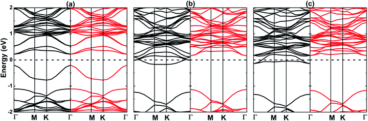 |
| | Fig. 8 Spin-polarized band structure (black line: spin-up; red line: spin-down) of (a) OV, (b) OF, and (c) OCl systems. | |
The illustration of the spin density given in Fig. 9 suggests that the magnetic properties of the doped systems are produced mainly by the Mo atoms. In the case of F doping, it can be noted an antiferromagnetic coupling since the magnetization of the first and second Mo atom from dopant site is because of a larger charge density in the spin-up channel and spin-down channel, respectively. On the contrary, the spin-up channel is the main contributor to the magnetism of the OCl system, indicating a parallel alignment, that is ferromagnetic coupling. The obtained magnetic moments are listed in Table 2. A value as large as of 0.42 (μB) is obtained for the second Mo atom in the OF structure, while two remaining Mo atoms exhibit quite smaller values. According to our calculations, Cl doping induces a weaker magnetization considering that the largest magnetic moment is 0.17 (μB), which is 59.52% smaller than that in the OF system. Also, making a reasonable comparison it can be concluded that the doping at S site may more efficient to magnetize the MoSO Janus monolayer, yielding magnetic systems with considerably larger magnetic moments than doping at the O site.
 |
| | Fig. 9 Spin density (blue surface: spin-up; yellow surface: spin-down) of (a) OF and (b) OCl (iso-surface of value 0.02) systems. | |
E. Formation and cohesive energy
Experimentally, the electron beam can create vacancies in the 2D TMDs, and the materials can be doped with a subsequent embedding impurity atoms in the vacancy sites.49 Keeping this two-step process in mind, we have calculated the formation energy Ef of defects using following formula:| |
 | (2) |
where the total energy of defective systems is denoted by Et; E(MoSO) is total energy of the pristine MoSO single layer; μ refers to the chemical potential of X (Mo, S, and O) and D (Al, Ga, F, and Cl) atoms; and A is area of the supercell. Results are given in Tables 1, 3, and 4. The calculated Ef of MoV, SV, and OV systems is 74, 31, and 45.80 (meV Å−2), respectively. These results indicate that the formation of S single vacancy is energetically more favorable than Mo and O single vacancies, similar feature has been observed in MoS2 single layer.50 Doping the MoSO monolayer with Al (at Mo site) and F (at S site) impurities may be exothermic processes since their formation energy takes negative values of −4.40 and −10.60 (meV Å−2), respectively. Moreover, the incorporation of halogen atoms into S site may requires smaller energy than into O site.
Table 4 Bond length d (Å), buckling height Δ (Å), interatomic angle ∠ (°), formation energy Ef (meV Å−2) and cohesive energy Ec (eV per atom) of the MoSO monolayer with defect at O-site (D = O in OV system; D = F in OF system; D = Cl in OCl system)
| |
dMo–S |
dMo–D |
ΔMo–S |
ΔMo–D |
∠SMoD |
Ef |
Ec |
| OV |
2.40 |
2.10 |
1.66 |
1.19 |
78.10 |
45.80 |
−3.98 |
| OF |
2.38 |
2.34 |
1.60 |
1.53 |
83.00 |
5.66 |
−4.01 |
| OCl |
2.39 |
2.57 |
1.60 |
1.86 |
88.27 |
24.29 |
−3.96 |
Finally, to examine the structural stability of the considered defective and doped systems we calculate their cohesive energy Ec using following formula:
| |
 | (3) |
Herein,
Et denotes the system total energy;
ni is the number of atom
i-th in the cell; and
E(
i) refers to the energy of an isolated
i atom. Results are listed in
Tables 1,
3, and
4. It can be concluded that all systems are structurally stable since their cohesive energies exhibit negative features. Considering the Mo site, the structure with a vacancy may be more stable than the those doped as suggested by its more negative
Ec value. A similar trend is noted when the S site is considered for studies. In contrast, negligible differences in cohesive energies are obtained for the O
V, O
F, and O
Cl systems, implying similar structural stability of these systems.
IV. Conclusions
In conclusion, the structural, electronic, and magnetic properties of the pristine and defected MoSO Janus monolayer have been systematically investigated using first-principles calculations. The MoSO single layer exhibits good dynamical and thermal stability. This is an indirect gap semiconductor, whose band structure is originated mainly from the interactions of Mo-4d, S-3p, and O-2p states. Its energy gap exhibits a strong strain-dependence reducing values with lattice tension and increasing values with lattice compression. Feature-rich electronic and magnetic properties can be obtained by either creating vacancy or doping. Specifically, the MoV–MoAl–MoGa and SF–SCl–OF–OCl structures are magnetic semiconductor and half-metallic 2D materials, respectively. Consequently, they exhibit significant magnetic properties, which are produced mainly by the spin-asymmetric Mo-4d orbital. These features make them promising 2D materials to create spin current for spintronic applications. While the non-magnetic semiconductor nature is obtained when creating a single S and O vacancy, the direct gap behavior and energy gap reduction suggest their prospect of optoelectronic applications. Our studies have introduced MoSO Janus monolayer to the family of Janus 2D materials, and pave a solid way to form novel multifunctional 2D materials for optoelectronic and spintronic applications. Therefore, results obtained herein may be used as a theoretical guidance for further experimental and theoretical investigations on Janus monolayers.
Conflicts of interest
The authors declare that they have no known competing financial interests or personal relationships that could have appeared to influence the work reported in this paper.
References
- K. S. Novoselov, A. K. Geim, S. V. Morozov, D. Jiang, Y. Zhang, S. V. Dubonos, I. V. Grigorieva and A. A. Firsov, Science, 2004, 306, 666–669 CrossRef CAS PubMed
 .
. - A. K. Geim, Science, 2009, 324, 1530–1534 CrossRef CAS PubMed .
- A. K. Geim and K. S. Novoselov, Nanoscience and technology: a collection of reviews from nature journals, World Scientific, 2010, pp. 11–19 Search PubMed .
- M. Chhowalla, Z. Liu and H. Zhang, Chem. Soc. Rev., 2015, 44, 2584–2586 RSC .
- S. Manzeli, D. Ovchinnikov, D. Pasquier, O. V. Yazyev and A. Kis, Nat. Rev. Mater., 2017, 2, 1–15 Search PubMed .
- Y. Yu, C. Li, Y. Liu, L. Su, Y. Zhang and L. Cao, Sci. Rep., 2013, 3, 1–6 Search PubMed .
- Y. Gong, Z. Lin, G. Ye, G. Shi, S. Feng, Y. Lei, A. L. Elias, N. Perea-Lopez, R. Vajtai and H. Terrones, et al., ACS Nano, 2015, 9, 11658–11666 CrossRef CAS PubMed .
- M. Amani, D.-H. Lien, D. Kiriya, J. Xiao, A. Azcatl, J. Noh, S. R. Madhvapathy, R. Addou, K. Santosh and M. Dubey, et al., Science, 2015, 350, 1065–1068 CrossRef CAS PubMed .
- H. Kim, D.-H. Lien, M. Amani, J. W. Ager and A. Javey, ACS Nano, 2017, 11, 5179–5185 CrossRef CAS PubMed .
- L. Liu, K. Ye, Z. Yu, Z. Jia, J. Xiang, A. Nie, F. Wen, C. Mu, B. Wang and Y. Li, et al., 2D Materials, 2020, 7, 025020 CrossRef CAS .
- J. Shi, D. Ma, G.-F. Han, Y. Zhang, Q. Ji, T. Gao, J. Sun, X. Song, C. Li and Y. Zhang, et al., ACS Nano, 2014, 8, 10196–10204 CrossRef CAS PubMed .
- C. Yelgel, Ö. Yelgel and O. Gülseren, J. Appl. Phys., 2017, 122, 065303 CrossRef .
- S. Mohammad Tabatabaei, M. Noei, K. Khaliji, M. Pourfath and M. Fathipour, J. Appl. Phys., 2013, 113, 163708 CrossRef .
- S. Ahmad and S. Mukherjee, et al., Graphene, 2014, 3, 52 CrossRef .
- L.-p. Feng, J. Su and Z.-t. Liu, J. Alloys Compd., 2014, 613, 122–127 CrossRef CAS .
- D. Cao, H. Shu, T. Wu, Z. Jiang, Z. Jiao, M. Cai and W. Hu, Appl. Surf. Sci., 2016, 361, 199–205 CrossRef CAS .
- X. Qiu, Y. Wang and Y. Jiang, Phys. Chem. Chem. Phys., 2021, 23, 11937–11943 RSC .
- M. Luo, Y. H. Shen and J. H. Chu, Jpn. J. Appl. Phys., 2016, 55, 093001 CrossRef .
- A.-Y. Lu, H. Zhu, J. Xiao, C.-P. Chuu, Y. Han, M.-H. Chiu, C.-C. Cheng, C.-W. Yang, K.-H. Wei and Y. Yang, et al., Nat. Nanotechnol., 2017, 12, 744–749 CrossRef CAS PubMed .
- J. Zhang, S. Jia, I. Kholmanov, L. Dong, D. Er, W. Chen, H. Guo, Z. Jin, V. B. Shenoy and L. Shi, et al., ACS Nano, 2017, 11, 8192–8198 CrossRef CAS PubMed .
- R. Sant, M. Gay, A. Marty, S. Lisi, R. Harrabi, C. Vergnaud, M. T. Dau, X. Weng, J. Coraux and N. Gauthier, et al., npj 2D Mater. Appl., 2020, 4, 1–8 CrossRef .
- D. Hoat, M. Naseri, N. N. Hieu, R. Ponce-Pérez, J. Rivas-Silva, T. V. Vu and G. H. Cocoletzi, J. Phys. Chem. Solids, 2020, 144, 109490 CrossRef CAS .
- S.-D. Guo, Y.-F. Li and X.-S. Guo, Comput. Mater. Sci., 2019, 161, 16–23 CrossRef CAS .
- Y. Guo, S. Zhou, Y. Bai and J. Zhao, Appl. Phys. Lett., 2017, 110, 163102 CrossRef .
- S. Zhou, C.-C. Liu, J. Zhao and Y. Yao, npj Quantum Mater., 2018, 3, 1–7 CrossRef .
- L. Hu and D. Wei, J. Phys. Chem. C, 2018, 122, 27795–27802 CrossRef CAS .
- H. Yang, P. Zhao, Y. Ma, X. Lv, B. Huang and Y. Dai, J. Phys. D: Appl. Phys., 2019, 52, 455303 CrossRef CAS .
- D. Hajra, R. Sailus, M. Blei, K. Yumigeta, Y. Shen and S. Tongay, ACS Nano, 2020, 14, 15626–15632 CrossRef PubMed .
- A. Bafekry, S. Karbasizadeh, C. Stampfl, M. Faraji, H. Do Minh, A. S. Sarsari, S. Feghhi and M. Ghergherehchi, Phys. Chem. Chem. Phys., 2021, 23, 15216–15223 RSC .
- A. C. Riis-Jensen, T. Deilmann, T. Olsen and K. S. Thygesen, ACS Nano, 2019, 13, 13354–13364 CrossRef CAS PubMed .
- M. N. Gjerding, A. Taghizadeh, A. Rasmussen, S. Ali, F. Bertoldo, T. Deilmann, N. R. Knøsgaard, M. Kruse, A. H. Larsen, S. Manti, T. G. Pedersen, U. Petralanda, T. Skovhus, M. K. Svendsen, J. J. Mortensen, T. Olsen and K. S. Thygesen, 2D Materials, 2021, 8, 044002 CrossRef .
- M. Demirtas, B. Ozdemir, Y. Mogulkoc and E. Durgun, Phys. Rev. B, 2020, 101, 075423 CrossRef CAS .
- M. Demirtas, M. J. Varjovi, M. M. Çiçek and E. Durgun, Phys. Rev. Mater., 2020, 4, 114003 CrossRef CAS .
- T. V. Vu, C. V. Nguyen, H. V. Phuc, A. Lavrentyev, O. Khyzhun, N. V. Hieu, M. Obeid, D. Rai, H. D. Tong and N. N. Hieu, Phys. Rev. B, 2021, 103, 085422 CrossRef CAS .
- D. K. Nguyen, D. Hoat, A. Bafekry, V. Van On, J. Rivas-Silva, M. Naseri and G. H. Cocoletzi, Phys. E, 2021, 131, 114732 CrossRef CAS .
- C.-Y. Xu, J.-K. Qin, H. Yan, Y. Li, W.-Z. Shao and L. Zhen, Appl. Surf. Sci., 2018, 452, 451–456 CrossRef CAS .
- M. Yagmurcukardes and F. Peeters, Phys. Rev. B, 2020, 101, 155205 CrossRef CAS .
- T. Wang, M. Su, H. Jin, J. Li, L. Wan and Y. Wei, J. Phys. Chem. C, 2020, 124, 15988–15994 CrossRef CAS .
- W. Kohn and L. J. Sham, Phys. Rev., 1965, 140, A1133 CrossRef .
- S. J. Clark, M. D. Segall, C. J. Pickard, P. J. Hasnip, M. I. Probert, K. Refson and M. C. Payne, Z. Kristallogr. Cryst. Mater., 2005, 220, 567–570 CrossRef CAS .
- J. P. Perdew, K. Burke and M. Ernzerhof, Phys. Rev. Lett., 1996, 77, 3865 CrossRef CAS PubMed .
- E. S. Kadantsev and P. Hawrylak, Solid State Commun., 2012, 152, 909–913 CrossRef CAS .
- X. Cui, Z. Kong, E. Gao, D. Huang, Y. Hao, H. Shen, C.-a. Di, Z. Xu, J. Zheng and D. Zhu, Nat. Commun., 2018, 9, 1–7 CrossRef CAS PubMed .
- Q.-l. Xiong, J. Zhou, J. Zhang, T. Kitamura and Z.-h. Li, Phys. Chem. Chem. Phys., 2018, 20, 20988–20995 RSC .
- A. E. Mikkelsen, F. T. Bölle, K. S. Thygesen, T. Vegge and I. E. Castelli, Phys. Rev. Mater., 2021, 5, 014002 CrossRef CAS .
- M. J. Varjovi, M. Yagmurcukardes, F. Peeters and E. Durgun, Phys. Rev. B, 2021, 103, 195438 CrossRef CAS .
- G. M. Stephen, I. McDonald, B. Lejeune, L. H. Lewis and D. Heiman, Appl. Phys. Lett., 2016, 109, 242401 CrossRef .
- X. Li and J. Yang, Wiley Interdiscip. Rev.: Comput. Mol. Sci., 2017, 7, e1314 Search PubMed .
- H.-P. Komsa, J. Kotakoski, S. Kurasch, O. Lehtinen, U. Kaiser and A. V. Krasheninnikov, Phys. Rev. Lett., 2012, 109, 035503 CrossRef PubMed .
- Y. Xu, Y. Li, X. Chen, C. Zhang, R. Zhang and P. Lu, AIP Adv., 2016, 6, 075001 CrossRef .
Footnote |
| † Electronic supplementary information (ESI) available. See DOI: 10.1039/d1ra05639e |
|
| This journal is © The Royal Society of Chemistry 2021 |
Click here to see how this site uses Cookies. View our privacy policy here. 
 Open Access Article
 This Open Access Article is licensed under a Creative Commons Attribution-Non Commercial 3.0 Unported Licence
 *de
*de


 . Results of the band structure and energy gaps are given in Fig. 3. From the left panel, one can see that in the considered energy range from −6% to 6%, this Janus monolayer retains its indirect gap semiconductor nature considering that the VBM and CBM are located at Γ and K point at a given strain, respectively. The band gap plots in the right panel indicate that this parameter decreases considerably when switching the strain nature from compressive to tensile. Note that the reduction rate is considerably smaller in the strain range from −6% to −4%, from which a nearly linear decreasing trend is obtained. MoSO monolayer exhibits an increase of 72.52(48.90)% up to a compressive strain strength of −6% as predicted by PBE(HSE6) potential, while a reduction of the order of −55.25(−40.66)% when the lattice tension of 6% is applied.