
 Open Access Article
 This Open Access Article is licensed under a Creative Commons Attribution-Non Commercial 3.0 Unported Licence
Computational insights into structural, electronic, and optical properties of Janus GeSO monolayer
Thi-Nga Doab,
Nguyen N. Hieu cd,
N. A. Poklonskie,
Nguyen Thi Thanh Binhf,
Cuong Q. Nguyencd and
Nguyen D. Hien*g
cd,
N. A. Poklonskie,
Nguyen Thi Thanh Binhf,
Cuong Q. Nguyencd and
Nguyen D. Hien*g
aLaboratory of Magnetism and Magnetic Materials, Advanced Institute of Materials Science, Ton Duc Thang University, Ho Chi Minh City, Vietnam. E-mail: dothinga@tdtu.edu.vn
bFaculty of Applied Sciences, Ton Duc Thang University, Ho Chi Minh City, Vietnam
cInstitute of Research and Development, Duy Tan University, Da Nang 550000, Vietnam. E-mail: hieunn@duytan.edu.vn
dFaculty of Environmental and Natural Sciences, Duy Tan University, Da Nang 550000, Vietnam
eFaculty of Physics, Belarusian State University, Minsk 220030, Belarus
fFaculty of Fundamental Sciences, Quang Binh University, Quang Binh, Vietnam
gInstitute of Applied Technology, Thu Dau Mot University, Binh Duong Province 75000, Vietnam. E-mail: nguyendinhhien@tdmu.edu.vn
First published on 23rd August 2021
Abstract
Although O is an element of chalcogen group, the study of two-dimensional (2D) O-based Janus dichalcogenides/monochalcogenides, especially their 1T-phase, has not been given sufficient attention. In this work, we systematically investigate the structural, electronic, and optical properties of 1T Janus GeSO monolayer by using the density functional theory. Via the analysis of phonon spectrum and evaluation of elastic constants, the GeSO monolayer is confirmed to be dynamically and mechanically stable. Calculated results for the elastic constants demonstrate that the Janus GeSO monolayer is much mechanically flexible than other 2D materials due to its small Young's modulus. At the ground state, while both GeS2 and GeO2 monolayers are indirect semiconductors, the Janus GeSO monolayer is found to be a direct band gap semiconductor. Further, effective masses of both electrons and holes are predicted to be directionally isotropic. The Janus GeSO monolayer has a broad absorption spectrum, which is activated from the visible light region and its absorption intensity is very high in the near-ultraviolet region. The calculated results not only systematically provide the fundamental physical properties of GeSO monolayer, but also stimulate scientists to further studying its importance both theoretically and experimentally.
1 Introduction
Two-dimensional (2D) systems have drawn great interest due to their outstanding physical properties.1,2 After the discovery of graphene in 2004,3 a series of other 2D materials have been intensively studied by both the theoretical and experimental methods.4,5 2D structures of silicene, phosphorene, h-boron nitride, germanane, or transitional metal dichalcogenides (TMDs) have been predicted to be promising candidates for next-generation electronic devices.6–10Janus 2D structure has recently emerged as a novel 2D material which has received widespread attention.11,12 Especially, breaking the lattice symmetry of Janus monolayer might enable a number of interesting effects. For example, graphene-based Janus structure, graphene formed by selective hydrogen decorations on one side of graphene has been shown theoretically to be ferromagnetic indirect bandgap semiconductor and suitable for UV optoelectronic applications.13 Isolation of partially hydrogenated single-sided graphene was demonstrated by Haberer et al.14 Following graphene, 2D Janus TMDs have been synthesized successfully and predicted to exhibit many remarkable quantum effects such as Weyl fermions,15 charge density wave,16 superconductivity,16 and novel excitonic and valleytronic phenomena.12,17–20
The out-of-plane asymmetric structure in Janus materials has been observed experimentally.11 Due to the lacking of mirror symmetry, Janus 2D-TMCs exhibit numerous exotic physical properties associated with wide-ranging electronic properties from metallic to semiconducting and even superconducting, making them potential candidate for various applications such as optoelectronics, spintronics and valleytronics.21–23 The evolving of the Janus monolayer structure from TMD by completely replacing one layer of chalcogen atoms by another group-VI element leads to asymmetric dipole distribution, which results in a “colossal vertical electric field” within the monolayer of the Janus structure and consequently opens up their new application fields.24,25 Beside the Janus structures of TMDs, Janus monochalcogenides have also been of great interest in recent years.26,27 Guo and co-worked demonstrated that the Janus group III monochalcogenides have much higher piezoelectric coefficients than that of the corresponding group-III monochalcogenide monolayers.28 These Janus structures have also been proven to have efficient photocatalytic performance.26 Janus group-III monochalcogenide XGaInY (X, Y = S, Se, and Te) monolayers show strong light absorption coefficients (>104 cm−1) in the visible and ultraviolet regions and suitable band edge positions for water splitting.29 Another novel family of Janus structures, GaInX2 (X = S, Se), present an external electric field tunable band and band edge positions, turning them into promising candidates in photocatalysis.30
Currently, Janus 2D materials based on group-IV dichalcogenides are studied thoroughly by different groups. In particular, Janus structure dichalcogenide monolayer of IV-group GeSSe is predicted with a high piezoelectric coefficient, small Young's modulus, and semiconducting nature, promising futuristic applications in energy harvesting, nanopiezoelectric field-effect transistors, atomically thin sensors, shear/torsion actuators, transducers, self-powered circuits in nanorobotics, electromechanical memory devices, biomedical, and other nanoelectronic applications.31 It is well known that oxygen exhibits a prominent electronegativity compared to other chalcogens. Such a characteristic might lead to a number of interesting physical properties in the MOX (M = Ge, Sn; X = S, Se, Te) Janus 2D materials. Recently, GeS2 monolayer has been found to be dynamically stable and show indirect semiconducting characteristics.31 Moreover, dynamical stability of T-GeO2 (in tetrahedral configuration) monolayer has been predicted by first-principle calculations.32 The thin layers of GeO2 has also been fabricated.33,34 Particularly, oxygenation of TMDs or monochalcogenides can create the O-based Janus structures, which have been theoretically demonstrated to display various novel physical properties.35–37
In this study, we investigate the structural, electronic, and optical properties of Janus GeSO monolayer by using the density functional theory. First, we will evaluate the relaxed structure of the GeSO monolayer and its dynamical and mechanical stabilities. The extraordinary electronic properties will be next considered. Finally, the unconventional optical response associated with the electronic structure will be explored.
2 Computational details
The calculations were performed within the density functional theory (DFT) implemented in the Quantum Espresso package.38 The projector augmented wave potentials are used for the DFT calculations to treat the interactions between the valence electrons and the core.39 The Perdew–Burke–Ernzerhof (PBE) functional in the generalized gradient approximation (GGA) is used to describe the exchange–correlation interaction. To describe accurately the electronic bands with the possible strong electron correlations, the Heyd–Scuseria–Ernzerhof functional (HSE06) is also used in the present work.40 The Grimme's DFT-D2 approach41 is performed to treat the long-range weak van der Waals interactions in the Janus material. The kinetic energy cutoff is set to be 500 eV for the plane waves included in the basis set and the force-convergence criterion is to be 0.001 eV Å−1. To eliminate any interactions between neighbor plates, we fix the vacuum space along the z direction being 20 Å. The Γ-centered k-point meshes of 15 × 15 × 1 were generated based on the Monkhorst–Pack scheme42 for the structural relaxation and evaluation of the electronic properties. The phonon dispersion curves are calculated by using density-functional perturbation theory (DFPT)43 based on the Quantum Espresso code.38 A large supercell of 6 × 6 × 1 was used for the phonon spectrum calculations to obtain accurate results.3 Results and discussion
3.1 Atomic structure and stability
The structure of the studied 2D materials can exist in several kinds of atomic crystal, including 2H and 1T, 1T′, and 3R structural phases.44 The 1T Janus GeSO monolayer can be constructed from 1T GeS2 or GeO2 monolayers. By replacing the top layer of S atoms with O atom, the 1T Janus GeSO can be built as shown Fig. 1(a). While the hexagonal structures of GeS2 and SnO2 monolayers belong to the P![[3 with combining macron]](https://www.rsc.org/images/entities/char_0033_0304.gif) m1 group, the 1T Janus GeSO monolayer belongs to the P3m1 space group. Due to the lack of mirror symmetry, the symmetry of the Janus GeSO monolayer is lower than that of GeS2 or GeO2 monolayer. The vertical asymmetry in GeSO is clearly seen through the large difference in bond lengths between Ge–S and Ge–O bonds. The Ge–S and Ge–O bond lengths are calculated to be 2.33 and 2.07 Å, respectively. Our calculated results demonstrated that the optimized lattice constant of the Janus GeSO is 3.19 Å, which is between the values of GeS2 (3.44 Å) and GeO2 (2.90 Å). The calculated structural parameters of 1T GeS2, GeO2, and GeSO monolayers are listed in Table 1.
m1 group, the 1T Janus GeSO monolayer belongs to the P3m1 space group. Due to the lack of mirror symmetry, the symmetry of the Janus GeSO monolayer is lower than that of GeS2 or GeO2 monolayer. The vertical asymmetry in GeSO is clearly seen through the large difference in bond lengths between Ge–S and Ge–O bonds. The Ge–S and Ge–O bond lengths are calculated to be 2.33 and 2.07 Å, respectively. Our calculated results demonstrated that the optimized lattice constant of the Janus GeSO is 3.19 Å, which is between the values of GeS2 (3.44 Å) and GeO2 (2.90 Å). The calculated structural parameters of 1T GeS2, GeO2, and GeSO monolayers are listed in Table 1.
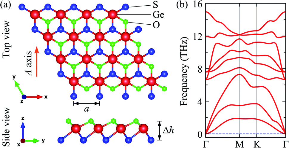 | ||
| Fig. 1 Optimized structure (a) and phonon spectrum (b) of the Janus GeSO monolayer. Red, blue, and green balls refer to the Ge, S, and O atoms, respectively. A axis is the axis along the armchair direction. | ||
| a | dGe–S | dGe–O | Δh | ϕ∠SGeS | ϕ∠OGeO | ϕ∠OGeS | |
|---|---|---|---|---|---|---|---|
| GeS2 | 3.44 | 2.43 | — | 2.79 | 89.73 | — | — |
| GeO2 | 2.90 | — | 1.94 | 1.95 | — | 83.04 | — |
| GeSO | 3.19 | 2.33 | 2.07 | 2.36 | — | — | 88.61 |
To examine the dynamical stability, we calculate the phonon dispersion of the Janus GeSO monolayer as presented in Fig. 1(b). The dynamical stability of materials can be evaluated via the analysis of their vibrational spectra. The stability of materials is confirmed if there are no imaginary frequencies in its phonon curves. The primitive cell of GeSO contains three atoms, therefore, its phonon spectrum has nine vibrational modes. Three acoustic modes are observed in the low-frequency region and six optical modes are in the higher frequencies. From Fig. 1(b), we can see that there is no gap between the acoustic and optical phonon branches. This leads to the strong acoustic-optical scattering in the GeSO monolayer, which may affect its thermal conductivity. More importantly, there are no imaginary frequencies in the phonon spectrum, suggesting that the Janus GeSO is dynamically stable and one can experimentally synthesis it as a free-standing monolayer.
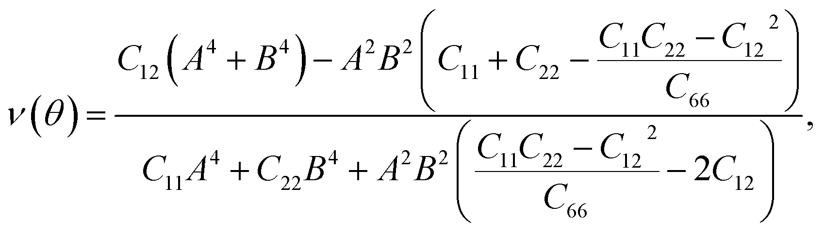
Further, the mechanical stability of the Janus GeSO monolayer is tested by calculating their elastic constants Cij. The elastic constants are key parameters that are directly related to the mechanical stability as well as the elastic properties of the material. As denoted by the Voigt notation, there are four independent elastic constants: C11, C22, C12, and C66. The angular-dependence of in-plane stiffness or 2D Young's modulus Y2D(θ) and Poisson's ratio ν(θ) can be written as the following31
 | (1) |
 | (2) |
![[thin space (1/6-em)]](https://www.rsc.org/images/entities/char_2009.gif) θ and B = cosθ with θ is the polar angle relative to the armchair axis (A axis in Fig. 1).
θ and B = cosθ with θ is the polar angle relative to the armchair axis (A axis in Fig. 1).
The Janus GeSO monolayer, as shown in Fig. 1, has hexagonal structure. Hence, we have C11 = C22 and the C66 can be obtained by expression C66 = (C11 − C12)/2. Therefore, there are only two independent elastic constants C11 and C12 needed. The Y2D, ν and 2D shear modulus G2D along the x or y direction for GeSO can be written as follows45
| Y2D = (C112 − C122)/C11; G2D = C66; ν = C12/C11. | (3) |
Obtained results for the elastic constants of GeS2, GeO2, and GeSO monolayers are listed in Table 2. The elastic constants of GeSO are calculated to be C11 = 88.16 N m−1 and C12 = 49.90 N m−1. The C11 of GeSO is smaller than that of both GeS2 and GeO2, while the Janus GeSO has higher C12 compared with GeS2 and GeO2. Importantly, the elastic constants of all three monolayers satisfy the Born criteria for mechanical stability46 that C11 > 0 and C112 − C122 > 0. It implies that these monolayers are mechanically stable. Our estimated Young's modulus of the Janus GeSO is 59.90 N m−1, which is comparable with that of Janus SnSSe monolayer (57.50 N m−1).47 We can see that the GeSO monolayer has a low in-plane stiffness compared to that of other 2D materials, such as MoS2 (130 N m−1),48 2D haeckelites (∼300 N m−1),49 2D ruthenium carbide (70.38 N m−1),50 2D PC3 (190 N m−1),51 and boron-carbon-nitride (291 N m−1).52 This suggests that the Janus GeSO monolayer is more flexible than those 2D structures and can withstand applied strain in large elongation. In Fig. 2, the angle-dependence of Young's modulus and Poisson's ratio of all three monolayers is illustrated in the polar diagram plot. Our calculated results demonstrate that the Y2D(θ) and ν(θ) in the polar diagram have a perfectly circular shape, suggesting that all monolayers GeS2, GeO2, and GeSO possess fully isotropic elastic properties. It is noted that most synthesized 2D structures possess hexagonal symmetry, therefore, they exhibit isotropic in-plane elastic properties.
| C11 (N m−1) | C12 (N m−1) | C66 (N m−1) | Y2D (N m−1) | ν | |
|---|---|---|---|---|---|
| GeS2 | 89.04 | 24.36 | 32.34 | 82.37 | 0.27 |
| GeO2 | 162.44 | 47.80 | 57.32 | 148.37 | 0.29 |
| GeSO | 88.16 | 49.90 | 19.13 | 59.90 | 0.57 |
 | ||
| Fig. 2 Polar diagram for the Young's modulus Y2D(θ) and Poisson's ratio ν(θ) of the Janus GeSO monolayer. θ is the angle relative to the A axis in Fig. 1. | ||
3.2 Electronic properties
Next, we investigate the electronic properties of the Janus GeSO monolayer. To improve the reliability of our calculation method, we first evaluate the band structure of the 1T-phase of pristine dichalcogenide monolayer GeS2. Our calculated results demonstrate that at the ground state, the GeS2 monolayer is an indirect semiconductor with a band gap of 0.74 eV at the PBE level. To correct the band gap, the HSE06 hybrid functional was used to evaluate the band structure of GeS2. The band gap of GeS2 is found to be 1.50 eV at the HSE06 level. Our calculated results are good in agreement with the available data (0.73/1.51 eV at the PBE/HSE06 level), which were very recently reported by Nandi and co-workers.31 This confirms that our computational method for electronic properties is valid. The calculated band structures of GeS2, GeO2, and GeSO monolayers are depicted in Fig. 3. It is seen that while both GeS2 and GeO2 monolayers are indirect semiconductors, the Janus GeSO monolayer exhibits direct semiconducting characteristics with both the conduction band minimum (CBM) and valence band maximum (VBM) located at the Γ symmetry point. There is a large difference in the calculated band gaps by the PBE and HSE06 methods. However, the evaluated band structures at the PBE and HSE06 levels are almost the same profiles as illustrated in Fig. 3. The band gap of the Janus GeSO monolayer is found to be 0.63 and 1.55 eV at the PBE and HSE06 levels, respectively. The band gap of GeSO is close to that of GeS2 but much smaller than that of GeO2 as listed in Table 1. The band gaps of the monolayers are also shown in Fig. 4 for comparison.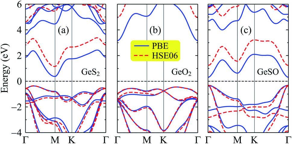 | ||
| Fig. 3 Electron band structures E(k) of GeS2 (a), GeO2 (b), and GeSO (c) monolayers calculated at the PBE and HSE06 levels in the first Brillouin zone. | ||
 | ||
| Fig. 4 Calculated band gaps of GeS2, GeO2, and GeSO by using PBE and HSE06 functionals. Filled and opened sharps refer to the indirect and direct gaps, respectively. | ||
To get insights into the formation of the electronic bands, especially the CBM and VBM, we show our evaluated weighted bands of the Janus GeSO in Fig. 5. It is found that the VBM is mainly contributed by the S-p orbital, while the Ge-s and Ge-p orbitals significantly contribute to the CBM of the Janus GeSO monolayer. In the higher energy regions, the O-p orbitals significantly contribute to both the valence and conduction bands.
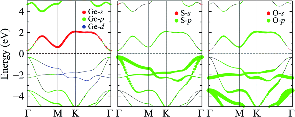 | ||
| Fig. 5 Calculated weighted bands of the Janus GeSO monolayer using the PBE functional. | ||
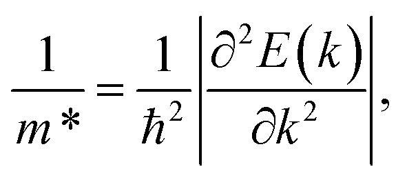
Moreover, we calculate the effective masses of the mobile carriers, which are also the key parameters of the materials. The effective masses of electron  and hole
  can be obtained by fitting parabolic function to the VBM and CBM through the formula as:
 | (4) |
 of GeSO is directionally isotropic along the x and y directions.
  along the kx∥x and ky∥y directions of GeSO is calculated to be 0.32m0 with m0 being the free electron mass. The small effective mass suggests that the carrier responds more quickly to the external field, leading to the high mobility of the carrier. Similarly, at the VBM, the lateral hole effective masses
  along the kx∥x and ky∥y directions are 1.24m0 and 1.28m0, respectively. These values suggest that the effective masses of both electrons and holes are directionally isotropic. This is due to the symmetry of the bands around the Γ symmetry point as depicted in Fig. 3(c). Compared with the GeS2 and GeO2 monolayers, as listed in Table 3, we can see that the carrier effective masses of GeS2 are directionally anisotropic. Meanwhile, for GeO2 monolayer, the effective mass of holes is directionally anisotropic and higher than that of electrons. This is due to the flat band around the VBM of GeO2 as depicted in Fig. 3(b).
 and hole
  along the x∥kx and y∥ky directions of GeS2, GeO2, and GeSO monolayers
| Eg (eV) |
|
|
Status | ||||
|---|---|---|---|---|---|---|---|
| PBE | HSE06 | x | y | x | y | ||
| GeS2 | 0.74 | 1.50 | 0.42 | 0.21 | 0.53 | 0.63 | Indirect |
| GeO2 | 3.60 | 5.40 | 0.35 | 0.35 | 4.45 | 3.82 | Indirect |
| GeSO | 0.63 | 1.55 | 0.32 | 0.32 | 1.24 | 1.28 | Direct |


3.3 Optical properties
Finally, we study the optical response of the Janus GeSO monolayer. The fundamental optical characteristics of the materials can be evaluated through the frequency-dependent complex dimensionless dielectric function, which is expressed as ε(ω) = ε1(ω) + iε2(ω). The imaginary part of the dielectric function ε2(ω) can be calculated as follows53
 | (5) |
The absorption coefficient A(ω) is given by55
 | (6) |
In this work, the dielectric function ε(ω) and absorption coefficient A(ω) of GeSO are evaluated along the x-direction by HSE06 method. The HSE06 method is investigated as a method that can give accurate results in calculations for optical characteristics of 2D materials.36,56 The ε(ω) and A(ω) of the Janus GeSO monolayer are illustrated in Fig. 6. It is noted that the static dielectric constant ε1(0) is inversely proportional to the direct bandgap of the semiconductor as described by the Penn model.57 The ε1(0) of the Janus GeSO monolayer is 1.99, which is smaller than that of the Janus SnSSe monolayer.47 As shown in Fig. 6, we can see that the absorption spectrum of the GeSO monolayer is activated in the visible light region (at 1.62 eV) which is consistent with its direct band gap at the HSE06 level. The first peak in the absorption spectrum is located at 3.69 eV as shown in Fig. 6(b). It is demonstrated that GeSO exhibits high absorption intensity in the ultraviolet region, around 9 eV. The maximum absorption coefficient of GeSO calculated by eqn (6) is 8.75 × 105 cm−1 at the photon energy of ℏω = 9.78 eV.
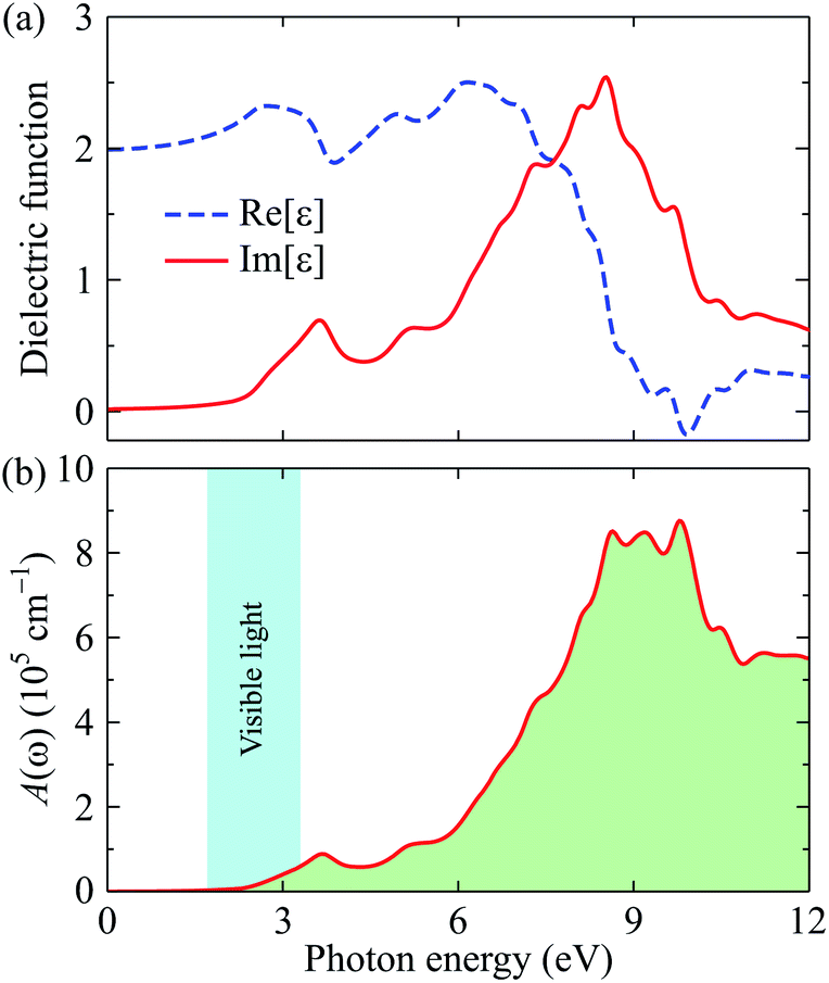 | ||
| Fig. 6 (a) Dielectric function ε(ω) and (b) optical absorption coefficient A(ω) of GeSO at the ground state. “Re” and “Im” in (a) refer to the real and imaginary parts of the dielectric function, respectively. | ||
4 Conclusion
In conclusion, we investigated the fundamental properties of the Janus GeSO by using the DFT calculations. Based on the analysis of phonon spectrum and elastic constants, it is found that the Janus GeSO monolayer is dynamically and mechanically stable at the ground state. The calculated results demonstrated that, with small elastic constants, the GeSO monolayer is more flexible than other 2D materials and that it can withstand the large-amplitude strain and is easily rolled to form nanotubes. The Janus GeSO is predicted to be the indirect semiconductor with a band gap being 0.63 and 1.55 eV at the PBE and HSE06 levels, respectively. We also explore the optical response of the Janus GeSO monolayer, which is calculated to be high absorption intensity in the ultraviolet region. Our findings not only systematically get insights into the physical properties of GeSO monolayer but also creates an important premise for further studies, especially creating a theoretical basis for the prospect of successfully synthesizing GeSO monolayer by experiment.Conflicts of interest
There are no conflicts to declare.Acknowledgements
This work is supported by the Belarusian National Research Program “Convergence-2025”.References
- N. A. Poklonski, S. A. Vyrko, A. I. Siahlo, O. N. Poklonskaya, S. V. Ratkevich, N. N. Hieu and A. A. Kocherzhenko, Mater. Res. Express, 2019, 6, 042002 CrossRef.
- A. I. Siahlo, N. A. Poklonski, A. V. Lebedev, I. V. Lebedeva, A. M. Popov, S. A. Vyrko, A. A. Knizhnik and Y. E. Lozovik, Phys. Rev. Mater., 2018, 2, 036001 CrossRef CAS.
- K. S. Novoselov, A. K. Geim, S. V. Morozov, D. Jiang, Y. Zhang, S. V. Dubonos, I. V. Grigorieva and A. A. Firsov, Science, 2004, 306, 666 CrossRef CAS PubMed.
- D. Muoi, N. N. Hieu, C. V. Nguyen, B. D. Hoi, H. V. Nguyen, N. D. Hien, N. A. Poklonski, S. S. Kubakaddi and H. V. Phuc, Phys. Rev. B, 2020, 101, 205408 CrossRef CAS.
- A. V. Lebedev, I. V. Lebedeva, A. M. Popov, A. A. Knizhnik, N. A. Poklonski and S. A. Vyrko, Phys. Rev. B, 2020, 102, 045418 CrossRef CAS.
- J. Zhuang, X. Xu, H. Feng, Z. Li, X. Wang and Y. Du, Sci. Bull., 2015, 60, 1551 CrossRef CAS.
- A. Carvalho, M. Wang, X. Zhu, A. S. Rodin, H. Su and A. H. Castro Neto, Nat. Rev. Mater., 2016, 1, 16061 CrossRef CAS.
- K. Zhang, Y. Feng, F. Wang, Z. Yang and J. Wang, J. Mater. Chem. C, 2017, 5, 11992 RSC.
- A. Acun, L. Zhang, P. Bampoulis, M. Farmanbar, A. van Houselt, A. N. Rudenko, M. Lingenfelder, G. Brocks, B. Poelsema, M. I. Katsnelson and H. J. W. Zandvliet, J. Phys.: Condens. Matter, 2015, 27, 443002 CrossRef CAS PubMed.
- S. Manzeli, D. Ovchinnikov, D. Pasquier, O. V. Yazyev and A. Kis, Nat. Rev. Mater., 2017, 2, 17033 CrossRef CAS.
- A.-Y. Lu, H. Zhu, J. Xiao, C.-P. Chuu, Y. Han, M.-H. Chiu, C.-C. Cheng, C.-W. Yang, K.-H. Wei, Y. Yang, Y. Wang, D. Sokaras, D. Nordlund, P. Yang, D. A. Muller, M.-Y. Chou, X. Zhang and L.-J. Li, Nat. Nanotechnol., 2017, 12, 744 CrossRef CAS PubMed.
- M. Yagmurcukardes, Y. Qin, S. Ozen, M. Sayyad, F. M. Peeters, S. Tongay and H. Sahin, Appl. Phys. Rev., 2020, 7, 011311 CAS.
- J. Zhou, Q. Wang, Q. Sun, X. S. Chen, Y. Kawazoe and P. Jena, Nano Lett., 2009, 9, 3867 CrossRef CAS PubMed.
- D. Haberer, C. E. Giusca, Y. Wang, H. Sachdev, A. V. Fedorov, M. Farjam, S. A. Jafari, D. V. Vyalikh, D. Usachov, X. Liu, U. Treske, M. Grobosch, O. Vilkov, V. K. Adamchuk, S. Irle, S. R. P. Silva, M. Knupfer, B. Büchner and A. Grüneis, Adv. Mater., 2011, 23, 4497 CrossRef CAS PubMed.
- J. Jiang, Z. Liu, Y. Sun, H. Yang, C. Rajamathi, Y. Qi, L. Yang, C. Chen, H. Peng, C.-C. Hwang, S. Sun, S.-K. Mo, I. Vobornik, J. Fujii, S. Parkin, C. Felser, B. Yan and Y. Chen, Nat. Commun., 2017, 8, 13973 CrossRef CAS PubMed.
- A. H. Castro Neto, Phys. Rev. Lett., 2001, 86, 4382 CrossRef CAS PubMed.
- J. R. Schaibley, H. Yu, G. Clark, P. Rivera, J. S. Ross, K. L. Seyler, W. Yao and X. Xu, Nat. Rev. Mater., 2016, 1, 16055 CrossRef CAS.
- M. Adhib Ulil Absor, H. Kotaka, F. Ishii and M. Saito, Jpn. J. Appl. Phys., 2018, 57, 04FP01 CrossRef.
- R. Peng, Y. Ma, S. Zhang, B. Huang and Y. Dai, J. Phys. Chem. Lett., 2018, 9, 3612 CrossRef CAS PubMed.
- B. Radisavljevic, A. Radenovic, J. Brivio, V. Giacometti and A. Kis, Nat. Nanotechnol., 2011, 6, 147 CrossRef CAS PubMed.
- K. F. Mak, C. Lee, J. Hone, J. Shan and T. F. Heinz, Phys. Rev. Lett., 2010, 105, 136805 CrossRef PubMed.
- X. Xu, W. Yao, D. Xiao and T. F. Heinz, Nat. Phys., 2014, 10, 343 Search PubMed.
- K. F. Mak, K. He, J. Shan and T. F. Heinz, Nat. Nanotechnol., 2012, 7, 494 CrossRef CAS PubMed.
- L. Dong, J. Lou and V. B. Shenoy, ACS Nano, 2017, 11, 8242 CrossRef CAS.
- C. Zhang, Y. Nie, S. Sanvito and A. Du, Nano Lett., 2019, 19, 1366 CrossRef PubMed.
- A. Huang, W. Shi and Z. Wang, J. Phys. Chem. C, 2019, 123, 11388 CrossRef CAS.
- T. V. Vu, V. T. T. Vi, H. V. Phuc, C. V. Nguyen, N. A. Poklonski, C. A. Duque, D. P. Rai, B. D. Hoi and N. N. Hieu, J. Phys.: Condens. Matter, 2021, 33, 225503 CrossRef CAS PubMed.
- Y. Guo, S. Zhou, Y. Bai and J. Zhao, Appl. Phys. Lett., 2017, 110, 163102 CrossRef.
- I. Ahmad, I. Shahid, A. Ali, L. Gao and J. Cai, RSC Adv., 2021, 11, 17230 RSC.
- H. Yang, P. Zhao, Y. Ma, X. Lv, B. Huang and Y. Dai, J. Phys. D: Appl. Phys., 2019, 52, 455303 CrossRef CAS.
- P. Nandi, A. Rawat, R. Ahammed, N. Jena and A. De Sarkar, Nanoscale, 2021, 13, 5460 RSC.
- Y. Guo, S. Zhang, T. Zhao and Q. Wang, Nanoscale, 2016, 8, 10598–10606 RSC.
- K. Okumura, K. Asakura and Y. Iwasawa, Langmuir, 1998, 14, 3607 CrossRef CAS.
- T. Hibino, M. Niwa, Y. Murakami and M. Sano, J. Chem. Soc., Faraday Trans. 1, 1989, 85, 2327 RSC.
- M. J. Varjovi, M. Yagmurcukardes, F. M. Peeters and E. Durgun, Phys. Rev. B, 2021, 103, 195438 CrossRef CAS.
- M. Demirtas, B. Ozdemir, Y. Mogulkoc and E. Durgun, Phys. Rev. B, 2020, 101, 075423 CrossRef CAS.
- T. V. Vu, C. V. Nguyen, H. V. Phuc, A. A. Lavrentyev, O. Y. Khyzhun, N. V. Hieu, M. M. Obeid, D. P. Rai, H. D. Tong and N. N. Hieu, Phys. Rev. B, 2021, 103, 085422 CrossRef CAS.
- P. Giannozzi, S. Baroni, N. Bonini, M. Calandra, R. Car, C. Cavazzoni, D. Ceresoli, G. L. Chiarotti, M. Cococcioni, I. Dabo, A. Dal Corso, S. de Gironcoli, S. Fabris, G. Fratesi, R. Gebauer, U. Gerstmann, C. Gougoussis, A. Kokalj, M. Lazzeri, L. Martin-Samos, N. Marzari, F. Mauri, R. Mazzarello, S. Paolini, A. Pasquarello, L. Paulatto, C. Sbraccia, S. Scandolo, G. Sclauzero, A. P. Seitsonen, A. Smogunov, P. Umari and R. M. Wentzcovitch, J. Phys.: Condens. Matter, 2009, 21, 395502 CrossRef PubMed.
- G. Kresse and D. Joubert, Phys. Rev. B: Condens. Matter Mater. Phys., 1999, 59, 1758 CrossRef CAS.
- J. Heyd, G. E. Scuseria and M. Ernzerhof, J. Chem. Phys., 2003, 118, 8207 CrossRef CAS.
- S. Grimme, J. Comput. Chem., 2006, 27, 1787 CrossRef CAS PubMed.
- H. J. Monkhorst and J. D. Pack, Phys. Rev. B: Solid State, 1976, 13, 5188 CrossRef.
- T. Sohier, M. Calandra and F. Mauri, Phys. Rev. B, 2017, 96, 075448 CrossRef.
- S. Das, J. A. Robinson, M. Dubey, H. Terrones and M. Terrones, Annu. Rev. Mater. Res., 2015, 45, 1 CrossRef CAS.
- R. C. Andrew, R. E. Mapasha, A. M. Ukpong and N. Chetty, Phys. Rev. B: Condens. Matter Mater. Phys., 2012, 85, 125428 CrossRef.
- F. Mouhat and F.-X. Coudert, Phys. Rev. B: Condens. Matter Mater. Phys., 2014, 90, 224104 CrossRef.
- S.-D. Guo, X.-S. Guo, R.-Y. Han and Y. Deng, Phys. Chem. Chem. Phys., 2019, 21, 24620 RSC.
- R. C. Cooper, C. Lee, C. A. Marianetti, X. Wei, J. Hone and J. W. Kysar, Phys. Rev. B: Condens. Matter Mater. Phys., 2013, 87, 035423 CrossRef.
- S. Thomas, H. Jung, S. Kim, B. Jun, C. H. Lee and S. U. Lee, Carbon, 2019, 148, 344 CrossRef CAS.
- S. Thomas and M. A. Zaeem, Appl. Surf. Sci., 2021, 563, 150232 CrossRef CAS.
- S. Jana, S. Thomas, C. H. Lee, B. Jun and S. U. Lee, Carbon, 2020, 157, 420 CrossRef CAS.
- S. Thomas and M. A. Zaeem, Phys. Chem. Chem. Phys., 2020, 22, 22066 RSC.
- A. Delin, P. Ravindran, O. Eriksson and J. M. Wills, Int. J. Quantum Chem., 1998, 69, 349 CrossRef CAS.
- H. Wang, G. Qin, J. Yang, Z. Qin, Y. Yao, Q. Wang and M. Hu, J. Appl. Phys., 2019, 125, 245104 CrossRef.
- P. Ravindran, A. Delin, B. Johansson, O. Eriksson and J. M. Wills, Phys. Rev. B: Condens. Matter Mater. Phys., 1999, 59, 1776 CrossRef CAS.
- H. L. Zhuang and R. G. Hennig, Appl. Phys. Lett., 2013, 103, 212102 CrossRef.
- D. R. Penn, Phys. Rev., 1962, 128, 2093 CrossRef CAS.
| This journal is © The Royal Society of Chemistry 2021 |