
 Open Access Article
 This Open Access Article is licensed under a Creative Commons Attribution-Non Commercial 3.0 Unported Licence
The ultralow thermal conductivity and tunable thermoelectric properties of surfactant-free SnSe nanocrystals†
Wasim J. Mir ab,
Anirudh Sharmaa,
Diego Rosas Villalvaa,
Jiakai Liub,
Md Azimul Haquea,
Semen Shikina and
Derya Baran*a
ab,
Anirudh Sharmaa,
Diego Rosas Villalvaa,
Jiakai Liub,
Md Azimul Haquea,
Semen Shikina and
Derya Baran*a
aKing Abdullah University of Science and Technology (KAUST), KAUST Solar Center (KSC), Physical Sciences and Engineering Division (PSE), Thuwal, 23955-6900, Saudi Arabia. E-mail: derya.baran@kaust.edu.sa
bKing Abdullah University of Science and Technology (KAUST), KAUST Catalysis Center (KCC), Division of Physical Science and Engineering (PSE), Thuwal, 23955-690, Kingdom of Saudi Arabia
First published on 19th August 2021
Abstract
Most studies to date on SnSe thermal transport are focused on single crystals and polycrystalline pellets that are obtained using high-temperature processing conditions and sophisticated instruments. The effects of using sub-10 nm-size SnSe nanocrystals on the thermal transport and thermoelectric properties have not been studied to the best of our knowledge. Here, we report the synthesis of sub-10 nm colloidal surfactant-free SnSe NCs at a relatively low temperature (80 °C) and investigate their thermoelectric properties. Pristine SnSe NCs exhibit p-type transport but have a modest power factor of 12.5 μW m−1 K−2 and ultralow thermal conductivity of 0.1 W m−1 K−1 at 473 K. Interestingly, the one-step post-synthesis treatment of NC film with methylammonium iodide can switch the p-type transport of the pristine film to n-type. The power factor improved significantly to 20.3 μW m−1 K−2, and the n-type NCs show record ultralow thermal conductivity of 0.14 W m−1 K−1 at 473 K. These surfactant-free SnSe NCs were then used to fabricate flexible devices that show superior performance to rigid devices. After 20 bending cycles, the flexible device shows a 34% loss in the power factor at room temperature (295 K). Overall, this work demonstrates p- and n-type transport in SnSe NCs via the use of simple one-step post-synthesis treatment, while retaining ultralow thermal conductivity.
Introduction
Thermoelectricity is an alternative and clean source of energy that involves interconversion between heat and electricity via the well-known Seebeck and Peltier effects.1,2 The thermoelectric efficiency of a material can be denoted by the dimensionless figure of merit ‘ZT’, which is established through the equation , where S, σ, and κ represent the Seebeck coefficient, electrical conductivity, and thermal conductivity, respectively. Attempts to increase the electrical conductivity often lead to an increase in the thermal conductivity for a typical semiconductor; hence, the maximum ZT involves a tradeoff between σ and κ at a given temperature.3–6 However, in the past 6 years, SnSe has emerged as a high-quality p-type thermoelectric material due to its low thermal conductivity (0.7–0.25 W m−1 K−1) over a broad temperature range of 300 K to 923 K.7–9 Interestingly, thermal transport is dominated by lattice phonons, which decrease in number with an increase in temperature. This leads to a breakthrough ZT value of 2.6 being shown by a SnSe single crystal with a lowest thermal conductivity of ∼0.25 at a temperature of 923 K.9–16 Further attempts to decrease the thermal conductivity and to tailor the thermoelectric performance of bulk SnSe at lower temperatures have been widely made. The doping/alloying of SnSe single crystals and pellets is mostly carried out at high temperatures of >300 °C; nevertheless, this represents a promising strategy for tuning the thermoelectric properties of bulk SnSe.9,12,15,17–20 Other innovative strategies like phase texturing and nanostructuring have also been studied.11,13,14,16,21–24 However, we note that nanostructured SnSe has mostly been studied in the form of pellets, where aggressive processing and sintering can lead to a decrease in the nanocrystalline aspect of domains. The phase texturing of SnSe with another phase such as SnSe2 presents challenges relating to controlling the growth of the two phases, and this is usually achieved via the time-dependent annealing of the film.14,25,26
On the other hand, sub-10 nm SnSe nanocrystals (NCs) could lead to the strong scattering of phonons at the grain boundaries and, hence, lower thermal conductivity.10,14,22,27,28 Recently, ultralow thermal conductivity of 0.08 W m−1 K−1 was reported by Burton et al. using nanostructured SnSe film, with the film obtained through an advanced thermal evaporation technique.10 However, nanostructured SnSe NCs show high thermal conductivities when processed in the form of pellets, probably due to loss of the nanocrystalline aspect of the grains.23,24,29–31 Therefore, it is important to carry out the soft processing of SnSe NCs in the form of films to preserve their nanocrystalline aspect and to achieve ultralow thermal conductivities, provided the films are made conductive enough. Interestingly, a recent report on polycrystalline SnSe films shows that via varying the feed ratio of the Se precursor, mixed-phase SnSe–SnSe2 can be obtained that exhibits superior performance and a high thermoelectric power factor (S2σ = ∼330 μW m−1 K−1) compared to its single crystal counterpart (S2σ = 300 μW m−1 K−1) at 300 K.8,14 It is likely that excess Se precursor oxidizes Sn2+ to Sn4+, leading to degenerate hole doping in the SnSe films. These findings motivated us to explore in detail the thermoelectric properties of SnSe NCs that are synthesized with excess Se2− precursor. The idea is that excess Se2− precursor on the surface of the SnSe NCs can stabilize the NCs against aggregation in polar solvents and may also partly oxidize Sn2+ to Sn4+.
In this manuscript, we first report the colloidal synthesis of SnSe NCs in the absence of insulating organic ligands at a relatively low temperature of 80 °C. Films derived from these surfactant-free NCs retain the nanocrystalline aspect of the grains. Pristine SnSe NCs show p-type transport, which switches to n-type after post-synthesis modification with methylammonium iodide (MAI), leading to a higher power factor. Photoelectron spectroscopy suggests that the incorporation of iodide ions into SnSe NCs leads to n-type doping in MAI-treated NCs. Thermal transport studies revealed thermal conductivities of 0.1 and 0.14 W m−1 K−1 in p- and n-type SnSe NCs, respectively, at 473 K, indicating that the p- to n-type transition preserves the ultralow thermal conductivity while improving the power factor. Interestingly, our work achieves a record ultralow thermal conductivity of 0.14 W m−1 K−1 at 473 K for n-type transport in SnSe NCs.
Experimental details
Materials
Tin(II) iodide anhydrous beads (SnI2, 99.99%, Sigma-Aldrich), sodium selenide (Na2Se, 99.8%, Alfa-Aesar), methylammonium iodide (MAI, 98%, Sigma-Aldrich), formamide (FA, ≥99.5%, Sigma-Aldrich), and acetonitrile (CH3CN, ≥99.5%, Sigma-Aldrich) were used. All chemicals are used as received without any additional purification.Synthesis of SnSe nanocrystals
The synthesis of SnSe NCs is carried out inside a glove box under N2 purging conditions. A solution of SnI2 (182 mg) in 5 mL of formamide is prepared via heating the vial up to 80 °C inside the glove box. At the same time, another solution of Na2Se (125 mg) in 1 mL of formamide is prepared and kept at room temperature. SnSe NCs are then synthesized via injecting 1 mL of Na2Se precursor solution into SnI2 solution maintained at 80 °C. The immediate appearance of a black-colored solution suggests the formation of SnSe NCs. The reaction was then allowed to proceed for 5 min, followed by natural cooling to room temperature inside the glove box. The crude solution containing NCs is washed via adding 6 mL of acetonitrile, then centrifuged at 5000 rpm for 5 min, and the obtained precipitate is redispersed in 1 mL of fresh formamide. The colloidal dispersion is passed through a filter with a pore size of 0.2 μm, and the filtrate containing SnSe NCs is stored for further use. The NCs in formamide can be washed again using the same acetonitrile at a 1![[thin space (1/6-em)]](https://www.rsc.org/images/entities/char_2009.gif) :1 v/v ratio, followed by spinning at 5000 rpm for 5 min. However, the second washing step does not improve the thermoelectric properties, rather it degrades the colloidal stability, and we do not suggest this step when making films.
:1 v/v ratio, followed by spinning at 5000 rpm for 5 min. However, the second washing step does not improve the thermoelectric properties, rather it degrades the colloidal stability, and we do not suggest this step when making films.
Film fabrication
Colloidal SnSe NCs were first centrifuged at 5000 rpm for 1 min to remove larger aggregates, and the supernatant was used to coat films on different substrates. The films were obtained via dynamic spin-coating inside a N2-filled glove box using a glass or Kapton substrate preheated at 200 °C. Typically, 60 μL of SnSe NC ink is dispensed on the hot substrate under spinning at 2000 rpm and it is kept spinning for 30 s. After coating with the NC ink, annealing is carried out at 200 °C for about 2 min. The above dynamic spin-coating procedure on a hot substrate followed by interlayer annealing is repeated 5 to 9 times to obtain the desired thickness of 200 to 400 nm. The p-type film thickness was maintained at 400 nm, while the n-type film thickness was restricted to 200 nm. Final annealing was carried out at 200 °C for 30 min inside the glove box.To obtain n-type films, the above-prepared film is treated with methylammonium iodide (MAI) solution (prepared by dissolving 10 mg of MAI in 1 mL of acetonitrile). Typically, 60 μL of MAI solution is dispensed on the SnSe NC film and kept for 30 s before spinning at 2000 rpm for another 30 s. The MAI-treated film is annealed at 200 °C for 2 min to dry the film.
Characterization
Steady-state optical absorption spectra of the NCs were obtained using transmission mode on quartz substrates employing a Cary 5000 UV-vis-NIR spectrometer (Agilent Technologies). The zeta potential of SnSe NCs dispersed in water was measured using nano-ZS90 apparatus from Malvern Instruments, U.K. Variable temperature-dependent electrical conductivity and Seebeck coefficient measurements were carried out using a Netzsch SBA 548 Nemesis thermoelectric set-up under a He environment. The thicknesses of the films were measured using a Tencor profilometer. X-ray diffraction patterns were obtained using a Bruker D8 ADVANCE diffractometer equipped with Cu Kα radiation (λ = 1.54 Å). Atomic force microscopy imaging was carried using Bruker Dimension Icon apparatus with a ScanAsyst instrument under tapping mode, and samples were made via drop-casting over Si substrates. Scanning electron images were captured using SEM apparatus (Carl Zeiss Auriga). Hall measurements of films were carried out on glass substrates (1 cm × 1 cm) using a Hall effect measurement system (Lake Shore 7700A) employing van der Pauw geometry at room temperature under a magnetic field of 10 kG. Transmission electron microscopy images were captured using a Titan ST D3187 instrument.Thermal conductivity measurements
Temperature-dependent in-plane thermal conductivity (‖κ) was measured using a thin film analyzer from Linseis. The setup uses a chip containing an alumina membrane with pre-patterned platinum heaters and thermometers; we used a Kapton mask to pattern the SnSe NC film on top of the membrane and Pt contacts of the chip following the spin-coating method previously described. The instrument uses the 3ω method to determine ‖κ. Thermal conductivity measurements were carried out under vacuum.XPS and UPS studies
Photoelectron spectroscopy (PES) measurements were performed in an ultrahigh vacuum chamber (∼10−10 mbar) using a hemispherical electron analyzer (Sphera II EAC 125 7-channeltron). The analyzer was calibrated with the Fermi edge of clean polycrystalline silver. UPS measurements were performed using the He I line (excitation energy of 21.22 eV) at a pass energy of 10 eV. The work functions of samples were determined from the secondary electron cut-off of the UPS spectra, as described elsewhere.32 All XPS measurements were performed using monochromatized Al Kα radiation (excitation energy of 1486.6 eV) operating at 15 kV. XPS survey and high-resolution spectra were recorded at pass energies of 40 eV and 10 eV, respectively, and are referenced to the carbon 1s peak at 285 eV.Results and discussion
Developing conducting films of SnSe NCs involves the challenge of electronic coupling between NCs to minimize the grain boundary resistance.33 Organic-surfactant-free SnSe NCs were prepared via a single-step process (Fig. 1), and the derived thin films of SnSe NCs showed strong electronic coupling.34 Typically, organic-capped NCs generate many defects upon ligand exchange with shorter ligands, which are detrimental to the electronic transport of charge carriers.33 In contrast, our surfactant-free NCs do not require an additional ligand exchange step for electronic coupling. These SnSe NCs are colloidally stable in highly dielectric solvents due to excess anions on the surface that provide an electrostatic force of repulsion against aggregation.34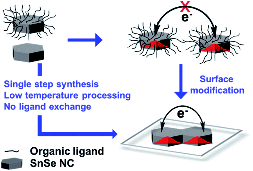 | ||
| Fig. 1 A schematic diagram showing that the development of organic-capped NCs into conductive films requires ligand exchange step to modify the surface of the NCs for efficient electronic coupling. However, organic-ligand-free NCs do not require an additional ligand exchange step when fabricating electronically coupled films. | ||
The SnSe NCs were prepared inside a glove box under purging conditions via employing a 5 min reaction at 80 °C. Details regarding the colloidal synthesis and film fabrication are presented in the experimental section. A colloidal dispersion of the SnSe NCs in formamide is stable for about a week and the films are stable under ambient air conditions for several months. To investigate the origin of the colloidal stability of the SnSe NCs, the zeta potential was measured (Fig. 2a). The SnSe NCs show a zeta potential of −37 mV, which suggests a negatively charged surface due to excess Se2− anions being present on the surfaces of the NCs. This negative charge on the surfaces of the SnSe NCs leads to electrostatic stabilization in polar solvents such as formamide.
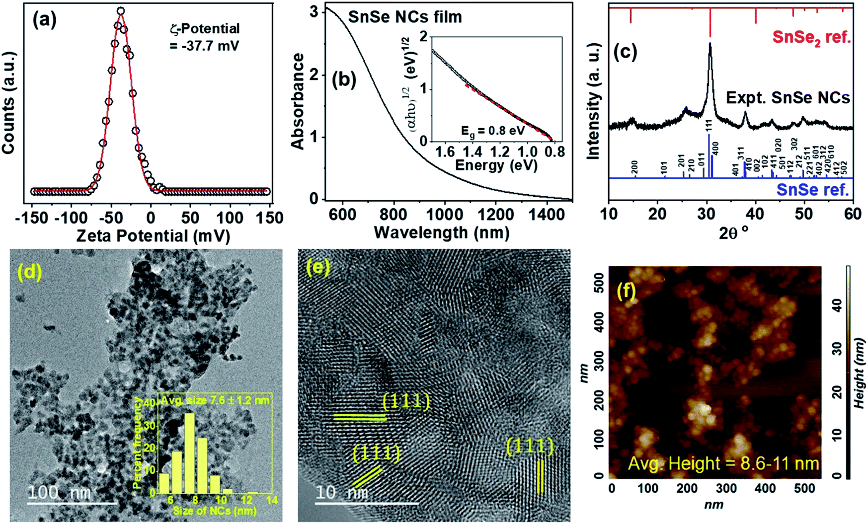 | ||
| Fig. 2 (a) The zeta potential of the SnSe NCs in formamide. (b) The optical absorbance of SnSe NCs that were coated over a quartz substrate; the inset shows the indirect bandgap obtained via Tauc plot fitting. (c) The XRD pattern of SnSe NCs along with the reference patterns of SnSe and SnSe2 phases. (d) A TEM image of organic-ligand-free SnSe NCs, obtained via drop-casting from formamide and drying at 80 °C; the inset shows the size distribution of the NCs, with an average size of 7.6 ± 1.2 nm. (e) A HRTEM image of NCs exhibiting lattice fringes, in which the (111) planes of the SnSe orthorhombic phase can be identified. (f) An AFM image of the SnSe NCs over a Si substrate, wherein the NCs display an average height of 8.6 to 11 nm. | ||
Fig. 2b shows the steady-state optical absorption of SnSe NCs deposited on a quartz substrate. The inset of Fig. 2b shows an extrapolated indirect bandgap of 0.8 eV obtained via Tauc plot fitting, and this bandgap is consistent with bulk SnSe.8 We note that annealing of the film at 200 °C is expected to increase the sizes of the NCs slightly and, hence, no quantum confinement effects are observed in the absorption spectrum of the NCs.
Fig. 2c shows the XRD pattern of SnSe NCs in comparison with reference SnSe and SnSe2 bulk patterns. The SnSe NCs were found to match with the orthorhombic phase of bulk SnSe, while the lack of impurity peaks in the experimental XRD pattern suggests that a phase-pure NC product was formed. Fig. 2d shows a transmission electron microscopy (TEM) image of the SnSe NCs, showing an average size of 7.6 ± 1.2 nm along with an elongated hexagonal shape, and the inset of Fig. 2d shows the size distribution. Please note that the SnSe NCs are agglomerated due to the absence of organic ligands that usually prevent the aggregation of NCs on the TEM grid. Fig. 2e shows a high-resolution (HR) TEM image of SnSe NCs with lattice fringes. An interplanar distance of 0.302 nm for various NCs is observed in Fig. 2e that corresponds to the (111) plane of the orthorhombic phase of SnSe. We also measured the height profile of the SnSe NCs via employing atomic force microscopy (AFM). Fig. 2f shows an AFM image of SnSe NCs, in which the NCs exhibit an average height of 8.6 to 11 nm (Fig. S1†).
Pristine SnSe NCs without any post-synthesis treatment exhibit p-type transport (Fig. 3a), similar to bulk SnSe.8 Upon one-step post-synthesis treatment with MAI, an effort initially made to improve the conductivity of film, we realize n-type transport in the SnSe NCs. Fig. 3b shows a field emission scanning electron microscopy (SEM) image of pristine NC film, and the inset of Fig. 3b shows a high-resolution SEM image (see Fig. S2† for SEM images of MAI-treated films). These SEM images suggest that the SnSe NC films have a uniform surface, and the NCs are densely packed with few pinholes. Notably, MAI treatment of the SnSe NCs does not degrade the film uniformity, and individual NCs retain the orthorhombic crystal structure of bulk SnSe (Fig. S3†).
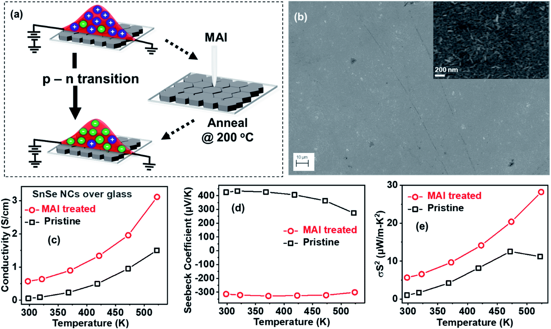 | ||
| Fig. 3 (a) A schematic diagram showing the p- to n-type transport realized in the SnSe NCs before and after treatment with MAI solution, respectively. (b) An FESEM image of pristine NC film on a glass substrate; the inset shows a high-resolution FESEM image of the film. The temperature-dependent thermoelectric properties of pristine and MAI-treated SnSe NCs: (c) electrical conductivity, (d) Seebeck coefficient, and (e) power factor. | ||
Fig. 3c shows the temperature-dependent conductivity of pristine and MAI-treated NC film over glass substrates. The conductivity increases with an increase in temperature, which is consistent with the semiconducting behavior of NCs similar to bulk SnSe. MAI treatment enhances the conductivity compared to pristine NCs and, more importantly, the semiconducting behavior is retained, unlike previous reports of the MAI treatment of PbS quantum dots.35 Fig. 3d shows the temperature-dependent Seebeck coefficients of NCs in the range of 300–525 K; both conductivity and the Seebeck coefficient were measured using a Netzsch Nemesis thermoelectric setup under a He environment. The pristine NCs show a positive Seebeck coefficient similar to bulk SnSe, wherein holes remain the majority charge carriers. However, the MAI treatment of NCs results in negative Seebeck coefficients, with electrons being the majority charge carriers. Although the Seebeck coefficient decreases in the MAI-treated NC films, the overall power factor increases compared to pristine SnSe NC films (Fig. 3e). The optimized threshold concentration for the p-to-n transition (Fig. S4 of the ESI†) was found to be 150 mM for 200 nm-thick NC film, which leads to the highest magnitude of Seebeck coefficient for n-type transport. A threshold concentration of ≥9 mM is required for 200 nm-thick film to realize a p-to-n type transition. The factors behind this p-to-n type transition in SnSe NCs with an increased power factor upon one-step MAI treatment are not clear and need to be studied in more detail. Pristine NCs show p-type transport with Hall mobility of 2.61 cm2 V−1 s−1 and a carrier concentration of 2.17 × 1017 cm−3 at 295 K (Fig. S5†). After MAI treatment, the negative Hall coefficient suggests that charge transport in the film is dominated by electrons. The Hall carrier concentration increases to 3.55 × 1018 cm−3, whereas the Hall mobility decreases to a value of 0.85 cm2 V−1 s−1 in MAI-treated NCs. Therefore, MAI treatment of NCs increases the carrier concentration by a factor of six but lowers the mobility by three compared to pristine SnSe NCs. The increases in conductivity and the power factor after the MAI treatment of NCs (Fig. 3c–e) can be attributed to the increase in the carrier concentration.
We then employed ultraviolet photoelectron spectroscopy (UPS) in combination with optical studies to figure out the electronic band structures before and after the MAI treatment of SnSe NCs. Fig. 4a shows that the onset of the work function for pristine and MAI-treated NCs remains unchanged at 4.8 ± 0.05 eV. In Fig. 4b, the valence band is plotted as a function of the binding energy. The density of states (DOS) at around 2.5 eV is significantly reduced after MAI treatment, and these observations were reproducible over glass and gold-coated Si/SiO2 substrates. The decrease in the DOS suggests a change in the valence electronic structure of the SnSe NCs after MAI treatment. In the case of pristine NCs, the valence band edge (Fig. 4c) was found to be 0.12 eV away from the Fermi level. Taking an optical band gap of 0.8 eV into account, UPS measurements predict p-type transport in pristine SnSe NCs, which is consistent with thermoelectric and Hall studies. After MAI treatment, the valence band in Fig. 4d was found to be 0.27 eV from the Fermi level, which suggests n-type doping. The estimated energy level diagrams for both pristine and MAI-treated NCs are shown in Fig. 4e. Clearly, XPS studies show that in the MAI-treated sample, the valence band moves away from the Fermi level compared to pristine NCs, which is consistent with the observed n-type doping after MAI treatment.
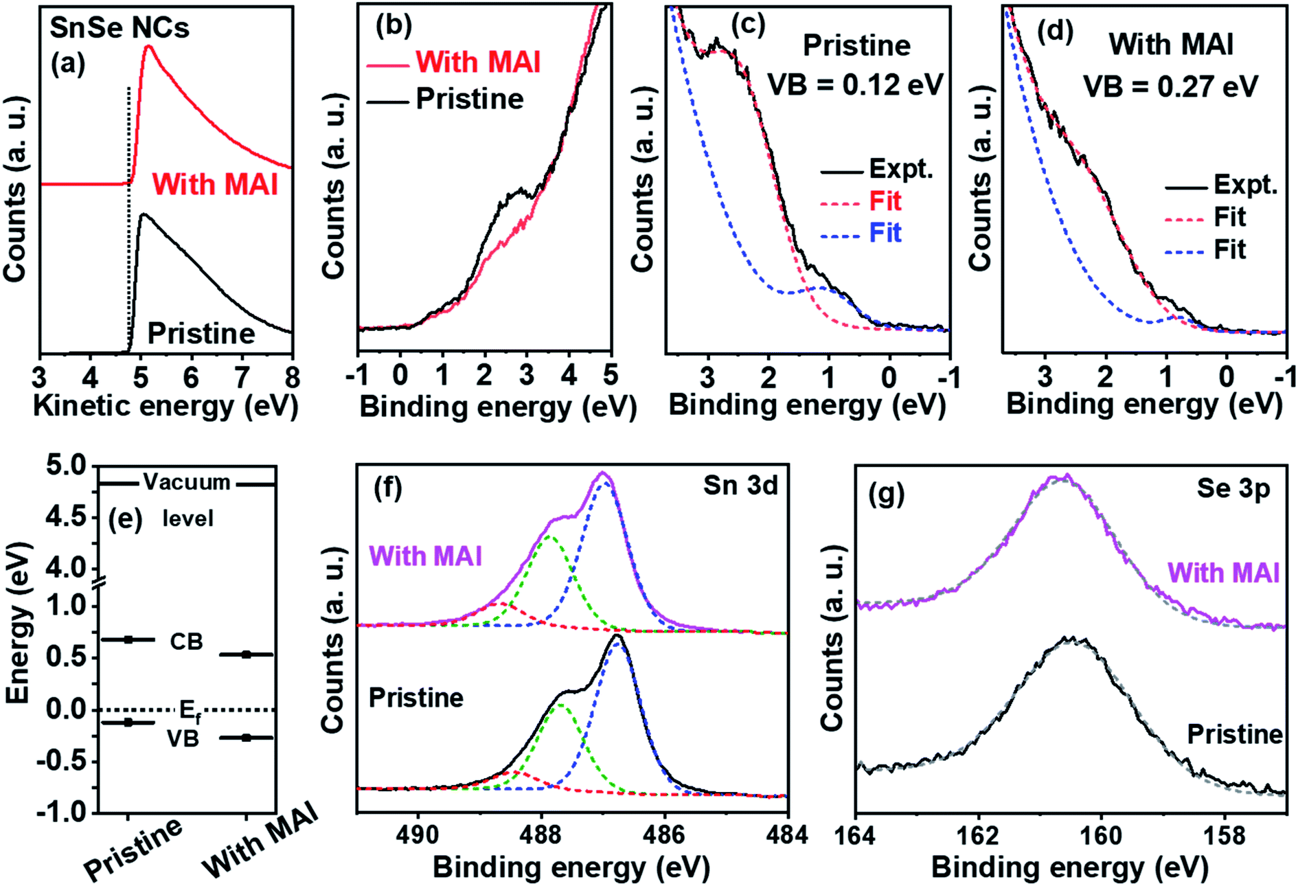 | ||
| Fig. 4 UPS measurements of pristine and MAI-treated SnSe NC films over glass substrates: (a) the secondary electron cut-off in the UPS spectra, (b) the valence region of the UPS spectra showing the change in the density of states at around 2.5 eV, demonstrated shifts in the valence band edge (c) before and (d) after MAI treatment, with respect to the Fermi level, and (e) experimentally estimated electronic band structures. High-resolution XPS spectra showing the (f) Sn 3d core levels, and (g) Se 3p core levels. The MAI-treated spectra/fits in panels f and g are shifted upwards for clarity of presentation. The dotted lines in panels c, d, f, and g are the Gaussian fitted curves, while the solid lines represent experimentally obtained data. | ||
To understand the origins of the shift in the Fermi level of the NCs after MAI treatment, XPS measurements were performed to further probe the induced changes in the chemical composition. The XPS survey spectra of NC films (Fig. S6†) deposited on a glass substrate exhibit three main elemental peaks corresponding to iodine, tin, and selenium, along with oxygen and carbon peaks. For the pristine NC thin film, a small symmetric I 3d5/2 peak at 620.7 eV was found, which can be attributed to remaining/unreacted SnI2 precursor in the SnSe NCs (Fig. S7†).36,37 When the SnSe NCs were treated with MAI, the iodine 3d peak was more pronounced and non-symmetric; the I 3d5/2 peak could be deconvoluted into two components at 620.4 eV and 621.2 eV (Fig. S7†), which are attributed to iodide ions bonded with Sn2+ and Sn4+, respectively.36,37 Detailed analysis of the high-resolution Sn 3d core level XPS spectra of the NCs is given in Fig. 4f. For pristine NCs, the Sn 3d5/2 peak could be deconvoluted into three components at binding energies of 486.8 eV, 487.7 eV, and 488.4 eV. The two components at 486.8 and 487.7 eV correspond to two oxidation states of Sn2+ and Sn4+, respectively, that are bonded to Se2−, and the third component at 488.4 eV is attributed to Sn4+ bonded with iodide.14,36,38 In the case of the MAI-treated NCs, the Sn 3d5/2 peak was also found to have three components, shifted by 0.2 eV towards higher binding energies, which was probably due to the increased oxidation of Sn2+ to Sn4+. Notably, these shifts are absent in Fig. 4g, which shows the Se 3p high-resolution XPS spectra of pristine and MAI-treated NCs. Therefore, the shift in the Sn 3d core levels could be due to the doping of SnSe with iodide ions upon MAI treatment. The excess doping of iodide ions in MAI-treated NCs increases the electron carrier concentration via promoting the oxidation of Sn2+ to Sn4+, hence leading to n-type doping.16,39
Interestingly, SnSe NCs can also achieve ultralow values of thermal conductivity via phonon scattering at the NC grain boundaries.8 Accordingly, we carried out thermal conductivity measurements using a chip-based 3ω technique.
Fig. 5a shows the variable temperature-dependent thermal conductivity of pristine SnSe NCs in comparison with MAI-treated NCs. Interestingly, both p- and n-type NCs show lower thermal conductivity values than the previously reported values for SnSe single crystals or solution-processed film/pellet samples.8,9,22,27,31 Ultralow thermal conductivities were observed in p-type SnSe NCs (0.19 to 0.1 W m−1 K−1) in the temperature region of 298–438 K. These values are the lowest figures achieved for solution-processed p-type SnSe NCs. On the other hand, MAI-treated n-type SnSe NCs showed slightly higher thermal conductivities of 0.2 to 0.14 W m−1 K−1 from 298 to 438 K. Interestingly, the ultralow thermal conductivity of 0.14 W m−1 K−1 at 438 K is a new record for n-type SnSe NCs. Please note that the thermal conductivity of 0.1 W m−1 K−1 achieved for p-type SnSe NCs is close to the previous record of 0.08 W m−1 K−1 for nanocrystalline SnSe film obtained via an advanced thermal evaporation technique.10 The decrease in thermal conductivity with an increase in temperature (Fig. 5a) suggests that thermal transport in the ensemble of NCs is dominated by phonons, similar to bulk SnSe.8 Notably, the thermal conductivity of n-type NCs also decreases with an increase in temperature. This suggests that the phonon bands of SnSe NCs remain unchanged after post-synthesis treatment with MAI solution. To confirm this, we measured the Raman spectra of SnSe NCs before and after MAI treatment (see Fig. S8 of the ESI†). The Raman spectra show two dominant phonon modes at 70 cm−1 and 184 cm−1 for both pristine and MAI-treated SnSe NCs.
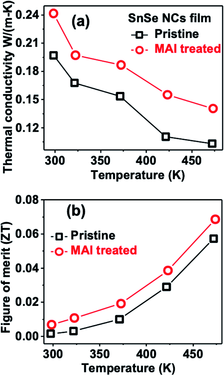 | ||
| Fig. 5 (a) Temperature-dependent in-plane thermal conductivity and (b) thermoelectric figure of merit (ZT) values for p- and n-type SnSe NCs. | ||
The above-measured thermal conductivity values were then used to calculate the thermoelectric figure of merit (ZT) of p- and n-type NCs in the low-temperature region from 298 to 473 K (Fig. 5b). Compared to p-type NCs, MAI-treated NCs show higher ZT values due to the higher power factor (Fig. 3e). A highest ZT value of ∼0.06 is observed at 473 K for pristine p-type SnSe NCs compared to a value of ∼0.07 for n-type NCs. We note that the ZT values of SnSe NCs are limited to low values due to the poor power factor of SnSe at low temperature (<500 K).8,9,11,16
Table 1 summarizes the thermoelectric properties at 300 K of SnSe NCs studied in this work and compares them with prior reports of SnSe films, polycrystalline pellets, and single crystals. SnSe NCs retain a high Seebeck coefficient for p-type and n-type transport at 300 K. The ultralow thermal conductivities of 0.19 and 0.24 W m−1 K−1 at 300 K for p- and n-type NCs, respectively, obtained through a solution process are the best figures reported so far. Finally, the ZT values at 300 K for the p- and n-type NCs are inferior to prior reports on SnSe pellets and single crystals. This is on account of the low power factor of the SnSe NCs and needs to be addressed in future work. In materials with low carrier concentrations, ZT is mainly governed by the power factor, which can be maximized via degenerate doping or alloying and the design of new heterostructures.
| Material, measurement conditions (process) | S (mV K−1) | Σ (S cm−1) | S2σ (mW m−1 K−1) | KT (W m−1 K−1) | ZT (300 K) | Ref. |
|---|---|---|---|---|---|---|
| SnSe thin film | ||||||
| SnSe, film (solution process) | 300 | 70 | ∼330 | — | — | 14 |
| SnSe, film (thermal evaporation) | 650 | 0.025 | 1 | 0.1 | 0.002 | 10 |
| SnSe NCs, film (solution process) | 424 | 0.05 | 1.03 | 0.19 | 0.001 | This work |
| SnSe NCs, film (solution process) | −314 | 0.6 | 5.6 | 0.24 | 0.007 | This work |
|
||||||
| SnSe pellets and single crystals | ||||||
| 6% Bi-doped SnSe, pellets (SPS process) | −220 | 1 | 70 | 0.3 | <0.01 | 11 |
| SnSe, hydrothermally synthesized pellets (SPS process) | 300 | 6 | 5 | 1.1 | <0.01 | 9 |
| SnSe, single crystal, (Bridgman synthesis) | 500 | 10 | 300 | 0.7 | 0.1 | 8 |
| 2.6 (923 K) | ||||||
| 3% I–SnSe1−xSx, high temperature pellets (hot-pressed) | −200 | 50 | <10 | 0.75 | <0.01 | 16 |
| SnSe, pellets (solution process) | 240 | 7 | 0.5 | — | — | 13 |
Finally, we extend the film fabrication of SnSe NCs over a flexible polyimide (Kapton) substrate to demonstrate high-quality and flexible SnSe NC films. Fig. 6a shows that the electrical resistance of the SnSe NC film increases after bending the film. However, the resistance of the film recovers to its initial value after releasing the bending stress. Accordingly, we carried out 20 bending cycles repeatedly and then measured the thermoelectric properties. Fig. 6b–d shows the electrical conductivity, Seebeck coefficient, and power factor, respectively, of n-type NCs before and after 20 bending cycles using NC film on a Kapton substrate. After 20 bending cycles, the film retains nearly 66% of the initial power factor at 295 K. We also note that the power factor of the n-type SnSe NCs on the polyimide substrate is 2 times higher compared to on a glass substrate at 295 K. As seen in the comparison in Fig. S9,† both p-type and n-type SnSe NCs showed higher power factors in flexible devices than their corresponding rigid devices at around room temperatures. This could be due to specific interactions between the surfactant-free SnSe NCs and polyimide substrate, leading to the oriented attachment and/or surface passivation of NCs.40,41 Such surfactant free NCs should be widely explored on different flexible substrates for thermoelectric applications.
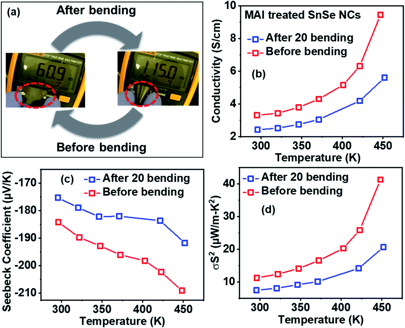 | ||
| Fig. 6 The thermoelectric properties of n-type MAI-treated SnSe NCs measured on a flexible Kapton substrate. (a) The electrical resistance of SnSe film increases after bending under stress, and this is reversible upon releasing the stress. Temperature-dependent thermoelectric parameters of NCs over Kapton before and after 20 bending cycles: (b) electrical conductivity, (c) Seebeck coefficient, and (d) power factor. | ||
Conclusions
In conclusion, we synthesized surfactant-free colloidal SnSe NCs at low temperature (80 °C) that are stabilized by excess Se2− anions. We then demonstrate a shift from p-type to n-type electronic transport in these NCs via performing one-step post-synthesis MAI treatment. UPS and optical studies suggest that the Fermi level shifts away from the valence band after post-synthesis MAI treatment compared to pristine NCs, leading to n-type doping. High-resolution XPS studies reveal that iodide doping in SnSe NCs leads to n-type transport in SnSe NCs. Interestingly, we observed ultralow thermal conductivities of 0.19 to 0.1 W m−1 K−1 in p-type SnSe NCs and 0.24 to 0.14 W m−1 K−1 in n-type NCs in the temperature range of 298 to 438 K. These numbers are the best for solution-processed SnSe NCs, with a new record ultralow thermal conductivity of 0.14 W m−1 K−1 for n-type SnSe NCs. Finally, we demonstrated a flexible SnSe NC film over a Kapton substrate that retains high performance after 20 bending cycles.Conflicts of interest
The authors declare no conflicts of interest.Acknowledgements
This publication is based upon work supported by the King Abdullah University of Science and Technology (KAUST) Office of Sponsored Research (OSR) under award no. OSR-CRG2018-3737 and OSR-2018-CARF/CCF-3079.References
- F. J. DiSalvo, Science, 1999, 285, 703 CrossRef CAS PubMed
.
- G. J. Snyder and E. S. Toberer, Nat. Mater., 2008, 7, 105–114 CrossRef CAS
- Z.-G. Chen, G. Han, L. Yang, L. Cheng and J. Zou, Prog. Nat. Sci.: Mater. Int., 2012, 22, 535–549 CrossRef
- C. B. Vining, Nat. Mater., 2009, 8, 83–85 CrossRef CAS
- C. J. Vineis, A. Shakouri, A. Majumdar and M. G. Kanatzidis, Adv. Mater., 2010, 22, 3970–3980 CrossRef CAS PubMed
- X. Chen, Z. Zhou, Y.-H. Lin and C. Nan, J. Materiomics, 2020, 6, 494–512 CrossRef
- A. T. Duong, V. Q. Nguyen, G. Duvjir, V. T. Duong, S. Kwon, J. Y. Song, J. K. Lee, J. E. Lee, S. Park, T. Min, J. Lee, J. Kim and S. Cho, Nat. Commun., 2016, 7, 13713 CrossRef CAS
- L.-D. Zhao, S.-H. Lo, Y. Zhang, H. Sun, G. Tan, C. Uher, C. Wolverton, V. P. Dravid and M. G. Kanatzidis, Nature, 2014, 508, 373–377 CrossRef CAS
- W. Wei, C. Chang, T. Yang, J. Liu, H. Tang, J. Zhang, Y. Li, F. Xu, Z. Zhang, J.-F. Li and G. Tang, J. Am. Chem. Soc., 2018, 140, 499–505 CrossRef CAS
- M. R. Burton, T. Liu, J. McGettrick, S. Mehraban, J. Baker, A. Pockett, T. Watson, O. Fenwickand and M. J. Carnie, Adv. Mater., 2018, 30, 1801357 CrossRef
- S. Chandra, A. Banik and K. Biswas, ACS Energy Lett., 2018, 3, 1153–1158 CrossRef CAS
- A. T. Duong, V. Q. Nguyen, G. Duvjir, V. T. Duong, S. Kwon, J. Y. Song, J. K. Lee, J. E. Lee, S. Park, T. Min, J. Lee, J. Kim and S. Cho, Nat. Commun., 2016, 7, 13713 CrossRef CAS
- G. Han, S. R. Popuri, H. F. Greer, J.-W. G. Bos, W. Zhou, A. R. Knox, A. Montecucco, J. Siviter, E. A. Man, M. Macauley, D. J. Paul, W.-g. Li, M. C. Paul, M. Gao, T. Sweet, R. Freer, F. Azough, H. Baig, N. Sellami, T. K. Mallick and D. H. Gregory, Angew. Chem., Int. Ed., 2016, 55, 6433–6437 CrossRef CAS PubMed
- S. H. Heo, S. Jo, H. S. Kim, G. Choi, J. Y. Song, J.-Y. Kang, N.-J. Park, H. W. Ban, F. Kim, H. Jeong, J. Jung, J. Jang, W. B. Lee, H. Shin and J. S. Son, Nat. Commun., 2019, 10, 864 CrossRef
- X. Shi, K. Zheng, M. Hong, W. Liu, R. Moshwan, Y. Wang, X. Qu, Z.-G. Chen and J. Zou, Chem. Sci., 2018, 9, 7376–7389 RSC
- Q. Zhang, E. K. Chere, J. Sun, F. Cao, K. Dahal, S. Chen, G. Chen and Z. Ren, Adv. Energy Mater., 2015, 5, 1500360 CrossRef
- C.-L. Chen, H. Wang, Y.-Y. Chen, T. Day and G. J. Snyder, J. Mater. Chem. A, 2014, 2, 11171–11176 RSC
- T.-R. Wei, G. Tan, X. Zhang, C.-F. Wu, J.-F. Li, V. P. Dravid, G. J. Snyder and M. G. Kanatzidis, J. Am. Chem. Soc., 2016, 138, 8875–8882 CrossRef CAS PubMed
- Z.-H. Ge, D. Song, X. Chong, F. Zheng, L. Jin, X. Qian, L. Zheng, R. E. Dunin-Borkowski, P. Qin, J. Feng and L.-D. Zhao, J. Am. Chem. Soc., 2017, 139, 9714–9720 CrossRef CAS PubMed
- A. Banik, T. Ghosh, R. Arora, M. Dutta, J. Pandey, S. Acharya, A. Soni, U. V. Waghmare and K. Biswas, Energy Environ. Sci., 2019, 12, 589–595 RSC
- G. Tang, W. Wei, J. Zhang, Y. Li, X. Wang, G. Xu, C. Chang, Z. Wang, Y. Du and L.-D. Zhao, J. Am. Chem. Soc., 2016, 138, 13647–13654 CrossRef CAS PubMed
- Y. Zhong, L. Zhang, V. Linseis, B. Qin, W. Chen, L.-D. Zhao and H. Zhu, Nano Energy, 2020, 72, 104742 CrossRef CAS
- H. Ju, M. Kim, D. Park and J. Kim, Chem. Mater., 2017, 29, 3228–3236 CrossRef CAS
- S. Chandra and K. Biswas, J. Am. Chem. Soc., 2019, 141, 6141–6145 CrossRef CAS PubMed
- Z.-G. Chen, X. Shi, L.-D. Zhao and J. Zou, Prog. Mater. Sci., 2018, 97, 283–346 CrossRef CAS
- S. R. Popuri, M. Pollet, R. Decourt, F. D. Morrison, N. S. Bennett and J. W. G. Bos, J. Mater. Chem. C, 2016, 4, 1685–1691 RSC
- Y. Feng, X. Zhang, L. Lei, Y. Nie and G. Xiang, RSC Adv., 2020, 10, 11990–11993 RSC
- J. J. Urban, Nat. Nanotechnol., 2015, 10, 997–1001 CrossRef CAS PubMed
- C.-H. Chien, C.-C. Chang, C.-L. Chen, C.-M. Tseng, Y.-R. Wu, M.-K. Wu, C.-H. Lee and Y.-Y. Chen, RSC Adv., 2017, 7, 34300–34306 RSC
- Z. Jian, H. Zhu, X. Wu, H. Cui, D. Li, J. Jiang, C. Gao, Q. Wang and Q. Cui, Nanoscale, 2015, 7, 10807–10816 RSC
- Y. Luo, Y. Zheng, Z. Luo, S. Hao, C. Du, Q. Liang, Z. Li, K. A. Khor, K. Hippalgaonkar, J. Xu, Q. Yan, C. Wolverton and M. G. Kanatzidis, Adv. Energy Mater., 2018, 8, 1702167 CrossRef
- A. Sharma, G. Andersson, J. Rivnay, J. F. Alvino, G. F. Metha, M. R. Andersson, K. Zuber and M. Fabretto, Adv. Mater. Interfaces, 2018, 5, 1800594 CrossRef
- D. V. Talapin, J.-S. Lee, M. V. Kovalenko and E. V. Shevchenko, Chem. Rev., 2010, 110, 389–458 CrossRef CAS
- K. P. Kadlag, M. J. Rao and A. Nag, J. Phys. Chem. Lett., 2013, 4, 1676–1681 CrossRef CAS PubMed
- M. I. Nugraha, H. Kim, B. Sun, S. Desai, F. P. G. de Arquer, E. H. Sargent, H. N. Alshareef and D. Baran, Adv. Energy Mater., 2019, 9, 1901244 CrossRef
- I. S. Zhidkov, D. W. Boukhvalov, A. I. Kukharenko, L. D. Finkelstein, S. O. Cholakh, A. F. Akbulatov, E. J. Juárez-Pérez, P. A. Troshin and E. Z. Kurmaev, J. Phys. Chem. C, 2020, 124, 14928–14934 CrossRef CAS
- G. Rajendra Kumar, H.-J. Kim, S. Karupannan and K. Prabakar, J. Phys. Chem. C, 2017, 121, 16447–16453 CrossRef CAS
- D. Ni, Y. Chen, X. Yang, C. Liu and K. Cai, J. Alloys Compd., 2018, 737, 623–629 CrossRef CAS
- A. Das, A. Chauhan, V. Trivedi, M. Tiadi, R. Kumar, M. Battabyal and D. K. Satapathy, Phys. Chem. Chem. Phys., 2021, 23, 4230–4239 RSC
- H.-m. Qian, Q. Zhao, B.-s. Dai, L.-j. Guo, J.-x. Zhang, J.-j. Liu, J.-t. Zhang and H.-s. Zhu, NPG Asia Mater., 2015, 7, e152 CrossRef CAS
- M. A. Boles, D. Ling, T. Hyeon and D. V. Talapin, Nat. Mater., 2016, 15, 141–153 CrossRef CAS
Footnote |
| † Electronic supplementary information (ESI) available: Additional supporting data like AFM, SEM, XRD, thermoelectric properties, Hall, XPS and Raman spectra. See DOI: 10.1039/d1ra05182b |
| This journal is © The Royal Society of Chemistry 2021 |