
 Open Access Article
 This Open Access Article is licensed under a Creative Commons Attribution-Non Commercial 3.0 Unported Licence
Prediction of allotropes of tellurium with molecular, one- and two-dimensional covalent nets for photofunctional applications†
Heng Zhang ab,
Junjie Wang*a,
Frédéric Guéganb,
Shuyin Yuc and
Gilles Frapper*ab
ab,
Junjie Wang*a,
Frédéric Guéganb,
Shuyin Yuc and
Gilles Frapper*ab
aState Key Laboratory of Solidification Processing, International Center for Materials Discovery, School of Materials Science and Engineering, Northwestern Polytechnical University, Xi'an, Shaanxi 710072, People's Republic of China. E-mail: wang.junjie@nwpu.edu.cn; heng.zhang@univ-poitiers.fr; Tel: +86-199-9190-9598 Tel: +86-159-3737-9685
bApplied Quantum Chemistry Group, E4, IC2MP, UMR 7285, Poitiers University, CNRS, 4 Rue Michel Brunet TSA 51106, 86073 Poitiers Cedex 9, France. E-mail: gilles.frapper@univ-poitiers.fr; frederic.guegan@univ-poitiers.fr; Tel: +33-6481-3241-3
cMSEA International Institute for Materials Genome, Jinxiu Rd. 1, Gu'an, Hebei 065500, People's Republic of China. E-mail: yusy@dianyunkeji.com; Tel: +86-180-0326-2785
First published on 10th September 2021
Abstract
In the present work, three new semiconducting two-dimensional (2D) Te phases containing three- and four-coordinated Te centers were proposed by using evolutionary algorithms combined with first-principles calculations. Using density functional theory calculations, we discussed the bonding and electronic properties in these phases, and subsequently rationalized their structures. The viability of these predicted structures was demonstrated by evaluating their thermodynamic, dynamic, mechanical, and thermal stabilities. Moreover, a significant direct band gap (0.951–1.512 eV) and excellent transport properties were evidenced in 2D Te nets, which suggests that they could be promising photovoltaic materials candidates. This is further supported by the stability of the associated bulk layered counterparts of the 2D Te nets.
1. Introduction
The successful isolation of graphene in 2004 opened a new realm of two-dimensional (2D) materials,1 due to its unique properties including high intrinsic mobility (200![[thin space (1/6-em)]](https://www.rsc.org/images/entities/char_2009.gif) 000 cm2 V−1 s−1), thermal conductivity (∼5000 W m−1 K−1), high specific surface area (2630 m2 g−1), high theoretical capacitance (550 F g−1) as well as its exceptional stability.2 Since then, 2D materials have attracted extensive interdisciplinary attention and many 2D materials were successfully fabricated, for example, hexagonal boron nitride, graphitic carbon nitride (g-C3N4), elemental 2D nanosheets (2D-Xenes), transition metal dichalcogenides (TMD), transition metal carbides and borides (MXenes, MBenes).3–9 Besides, the development of computing algorithms and facilities are significantly accelerating the pace of the discovery of 2D materials.10–12 In 2018, high-throughput calculations identified thousands of easily or potentially exfoliable three-dimensional (3D) layered compounds and more than 30 different prototypes in 2D crystal structures.13,14 Seeking for novel 2D structures falling outside known prototypes and exploring their potential applications in the optoelectronics, photovoltaic, energy storage and catalysis fields are the on-demand and emerging tasks of materials research.15–18
000 cm2 V−1 s−1), thermal conductivity (∼5000 W m−1 K−1), high specific surface area (2630 m2 g−1), high theoretical capacitance (550 F g−1) as well as its exceptional stability.2 Since then, 2D materials have attracted extensive interdisciplinary attention and many 2D materials were successfully fabricated, for example, hexagonal boron nitride, graphitic carbon nitride (g-C3N4), elemental 2D nanosheets (2D-Xenes), transition metal dichalcogenides (TMD), transition metal carbides and borides (MXenes, MBenes).3–9 Besides, the development of computing algorithms and facilities are significantly accelerating the pace of the discovery of 2D materials.10–12 In 2018, high-throughput calculations identified thousands of easily or potentially exfoliable three-dimensional (3D) layered compounds and more than 30 different prototypes in 2D crystal structures.13,14 Seeking for novel 2D structures falling outside known prototypes and exploring their potential applications in the optoelectronics, photovoltaic, energy storage and catalysis fields are the on-demand and emerging tasks of materials research.15–18
Tellurium (Te) is a semimetal located in the p-block of the periodic table and widely used in the fields of thermoelectronics, piezoelectronics and biomedicine taking advantage of its high photoconductivity, thermoelectricity, piezoelectricity and spectroscopic properties.19–21 Rich coordination environments of Te atoms in bulk allotropes were unveiled experimentally under pressure.22,23 The ground-state Te crystalizes in the rhombohedral space group (SG) P3121, consisting of one-dimensional (1D) helical chains with a coordination number (CN) of 2, i.e., CN = 2.20,24 However, when the external pressure goes to around 27 GPa, series of phase transitions are observed experimentally and then the CN of Te atom in the solid structures increases to 3, 4, 6 and 8.25–28 Due to the weak van der Waals (vdW) interaction between helical chains in P3121 Te phase at ambient condition, investigations of Te-based nanomaterials were mostly focused on one-dimensional (1D) nanostructures, for example, Te nanowires, nanobelts and nanotubes.29,30 In addition, large-sized Te films and nanoflakes with the thickness up to tens of nanometers were successfully obtained in the bulk arrangement through liquid-phase exfoliation method,31 molecule beam epitaxy,32 substrate-free solution process and topo-chemical transformation strategy.33–36 Fabricated Te films were reported with excellent performance,32–35 for example, in 2018, Te field-effect transistors with thickness of 16 nm were reported to be air-stable at room temperature for over two months with on/off ratios on the order of 106 and field-effect mobility of about 700 cm2 V−1 s−1.33
What about tellurium layered structures? In group VI elements, sulphur and selenium form several molecular allotropes (0D) at ambient conditions, but tellurium crystallizes in one single phase, i.e., the discussed grey selenium type P3121 phase. None of the group VI experimental structures present a 2D covalent framework and thus, no hypothetical 2D structure of Te may be built based on a structural analogy with isovalent compounds. Since 2017, theoretical and experimental interests were extended to elemental 2D group VI materials and diverse types of 2D Te covalent phases (α, β, γ, ε, η, δ, square-Te) and their multi-layered derivatives were theoretically proposed with remarkable stability by combining particle-swarm optimization methods and density functional theory calculations.37–42 Among those, both α and β-Te phases were successfully fabricated through use of a substrate-free solution process and an anisotropic ultrasonication method.33,36,42–44 Herein, based on the diverse phases of bulk Te under the high pressure induced by the multivalency,25–28 it is believed that Te may have more 2D allotropes besides the above proposed 2D covalent phases. Thus, our first aim in this study was to perform a full crystal structure prediction (CSP) of the possible 2D Te structures and our CSP searches revealed three semiconducting 2D Te nets (1, 2, 3). However, during this study, another team reported 31 different 2D Te nets.45 Our CSP searches agree well with this study, nevertheless, we found that the physical properties and electronic structures of these phases were left unexplored. In the present study, we then decided to investigate the structure topology by chemical bonding analysis and then further explore the electronic properties, optical absorptions, carrier mobilities and band alignments in those 2D Te nets for their potential photofunctional applications. Results shows that the simple electron count and VSEPR rule can well explain the bonding stability and semiconducting electronic properties in 2D Te nets.
2. Methods
Ab initio evolutionary structure prediction algorithm USPEX was employed to a systematic bulk and 2D CSP with the limit of 32 Te atoms per unit cell.46–50 For the fixed-composition CSP search on 2D Te crystals, 1.5 Å is chosen for the initial layer thickness. The technical details of USPEX calculations are given in ESI.†The projector-augmented-wave method was used for the structure relaxation as implemented in the Vienna ab initio simulation package (VASP).51,52 The valence electron configurations considered in the calculation is Te (5s25p4). The Perdew–Burke–Ernzerhof (PBE) exchange-correlation functional with the semiempirical vdW correction based on Grimme scheme (DFT-D2) was used to account for vdW interaction between the atomic layers.53,54 The plane-wave cutoff energy was set as 600 eV and the convergence for energy was chosen as 10−5 eV between two ionic steps. The structural optimization was done until the Hellmann–Feynman force acting on each atom was less than 0.01 eV Å−1. The Brillouin zone integrations were performed using Monkhorst–Pack sampling grids with resolution of 2π × 0.04 Å−1.55 The Heyd–Scuseria–Ernzerhof (HSE06) hybrid functional was adopted to get a reliable estimation of band gaps for semiconducting 2D Te structures, based on the DFT-D2 optimized structures.56 Moreover, to avoid the interaction of neighboring layers, a vacuum spacing of 20 Å was used for structural relaxation.
Ab initio molecular dynamics (AIMD) simulations at 300 K, 500 K based on density functional theory (DFT) are also carried out using VASP code to examine the thermal stability of 2D Te phases. The dynamic stability was checked through phonon dispersion calculations using density functional perturbation theory (DFPT), as implemented in the Phonopy program.57 In addition, the effect of zero-point energy (ZPE) on the stability of Te allotropes is considered. The incorporation of ZPE corrections has a very slight, if any, effect on the relative energies (see ESI†). Thus, the energies presented herein are not ZPE corrected. To perform chemical bonding analysis, the bond order was computed in the Chargemol program using the Manz' bond order equation with DDEC6 partitioning.58–61 Additionally, density of states (DOS), crystal overlap Hamilton population (COHP, using LOBSTER package),62,63 Bader charge,64 electron localization function (ELF),65 and partial (band decomposed) charge density from the optimized geometries were also analysed. Images of the crystalline structures are produced using VESTA software.66 Additional details for AIMD simulations, phonon dispersions and mechanical properties calculations are provided in Methodology part in ESI.†
Finally, the intrinsic carrier mobilities u in 2D Te nets 1, 2 and 3 were investigated within the framework of the deformation potential theory for semiconductors proposed by Bardeen and Shockley.67,68 The calculation details are explained in Methodology part in ESI.†
3. Results and discussion
3.1. Bulk Te phases
First, we looked for the low-lying forms of bulk elemental tellurium and hypothetical allotropes to validate our CSP methodology of combining an evolutionary algorithm implemented in USPEX code with first-principles calculations and to explore the full energy landscape of tellurium. Our CSP searches led to the identification of three bulk Te phases (P3121, R![[3 with combining macron]](https://www.rsc.org/images/entities/char_0033_0304.gif) , and P21/c Te) within an energy window of 98 meV per atom. Their crystal structures are displayed in Fig. 1, while their crystallographic parameters and enthalpies are listed in Tables S1 and S2 (ESI).† Additionally, it was found that they are all local minima on the potential energy surface (PES), i.e., no imaginary frequency appears in their phonon band structures shown in Fig. S1 in ESI.†
, and P21/c Te) within an energy window of 98 meV per atom. Their crystal structures are displayed in Fig. 1, while their crystallographic parameters and enthalpies are listed in Tables S1 and S2 (ESI).† Additionally, it was found that they are all local minima on the potential energy surface (PES), i.e., no imaginary frequency appears in their phonon band structures shown in Fig. S1 in ESI.†
 | ||
| Fig. 1 Structures of ground-state bulk P3121 Te phase (a–c) and predicted hypothetical Te allotropes (d and e): (a) side view of helical polymeric chain; (b) top view along the helices in the hexagonal unit cell; (c) view of distorted fused Te6 cubes; top view of (d) R Te and (e) P21/c Te. In (d) and (e), the motifs of Te6 and Te8 rings are also depicted. The brown balls indicate the Te atoms. | ||
Our CSP searches located the experimental grey P3121 Te (SG 152, Z = 3) structure as the ground-state phase and our optimized lattice parameters are a = 4.338 Å and c = 6.031 Å, in line with the experimental data (a = 4.457 Å and c = 5.927 Å).69 In bulk P3121 Te phase, two-coordinated Te atoms form helical polymeric chains running along [001] direction and the dihedral angle along the chain was computed as 100.6° (Fig. 1(a)). The Te–Te distance is 2.89 Å within the chain, a typical value of a single bond, while the valence angle is 103.0° (sp2 Te). Each atom has four more adjacent atoms from three different neighbouring chains at the distance of 3.40 Å, as depicted in Fig. 1(b). These interchain Te–Te distances are only 18% longer than the intrachain Te–Te distances (covalent bonding) and are significantly shorter than the van der Waals diameter of Te atom (4.12 Å). Thus, in bulk P3121 Te phase, there are two nearest and four next nearest bonds around each Te atom and then the helical chain structure of tellurium may be visualized as a distortion of the simple cubic lattice in Fig. 1(c). The four Te–Te contacts between neighbouring chains were proposed as coordinate covalent bonds, stemming from the lone pairs of electrons of Te atoms.69 The bonding interactions in P3121 Te can be also understood using band theory: starting from the β-Po structure, a Peierls distortion takes places that singles out two bonds per atom.70 Additionally, the bond strength of the different Te–Te bonds was indicated by the bond order, 0.75 for two short Te–Te contacts (2.89 Å), and 0.31 for four long Te–Te contacts (3.40 Å). Notice that external pressure causes the interatomic distances to approximate each other until finally every tellurium atom has six equidistant neighbouring atoms.19 What is more, the exfoliation energy of tellurium helical polymeric chain Te1D related from P3121 Te was computed as 415 meV per atom and may give an indication of the minimum energy needed to exfoliate a 2D net from a bulk crystal in tellurium chemistry.
Band structure of P3121 Te phase at the HSE06 level of theory in Fig. S2 (ESI)† shows that the VBM and CBM are both located in high-symmetry k-point H in the Brillouin zone. Thus, the ground-state Te bulk is a direct semiconductor with a band gap of 0.326 eV at HSE06 level, which is very close to the experimental value of 0.335 eV.24 Calculated DOS in Fig. S2† shows that the 5p orbitals of Te atoms dominate the states close to the Fermi energy and the lower bands are mainly composed of 5s orbitals.71 All these structural and electronic properties results validate our methodological choice to optimize tellurium allotropes and to evaluate energy gaps.
Moreover, for the first time, our CSP searches identified two new molecular crystals, R Te phase (SG 148, Z = 18) and P21/c Te phase (SG 14, Z = 64), that lie at 21 and 98 meV per atom above the ground-state bulk P3121 Te, respectively. Bulk R Te structure consists of stacked chair six-membered Te6 rings (shortest Te–Te distances in range 2.74–2.85 Å), isostructural to bulk elemental S6.72 P21/c Te phase corresponds to isostructural γ-Se8 shown in Fig. 1,73 in which there are crown-shaped Te8 rings stacked by the vdW interaction.
However, stating the obvious, no 2D tellurium net stemmed yet from our bulk CSP search. Moreover, none of the group VI experimental structures presents a 2D covalent framework. A few allotropes have 0D covalent nets, i.e., molecular X6 and X8 rings, and 1D – infinite helical chains – nets. Thus, no hypothetical 2D Te structure could be built based on a structural analogy of isovalent compounds. Therefore, we continued our tracking of novel 2D covalent Te nets by using a dedicated evolutionary algorithm designed to build layers,46–50 i.e., 2D materials. The results are discussed in the next section.
3.2 In silico 2D Te nets
Besides the seven already proposed two-dimensional Te nets, α-Te (Pm1, SG 164, Z = 3),42 β-Te (P2/m, SG 10, Z = 3),42 γ-Te (P![[6 with combining macron]](https://www.rsc.org/images/entities/char_0036_0304.gif) m2, SG 187, Z = 3),42 ξ-Te (P4/mmm, SG 123, Z = 3),40 δ-Te (Pma2, SG28, Z = 6),41 η-Te (P2221, SG17, Z = 6),41 and square-Te (P4/nmm, SG 129, Z = 2),37 a novel 2D crystal structure was found to locate on the PES generated by USPEX, namely 1. Besides, another two (unnamed) 2D crystal structures 2 and 3 were reconfirmed.41 Three 2D Te nets are shown in Fig. 2 and the calculated enthalpies and optimized crystallographic parameters of those three 2D Te allotropes are listed in Tables S3 and S4.† The calculated lattice parameters agree well with those reported in the previous work.45
m2, SG 187, Z = 3),42 ξ-Te (P4/mmm, SG 123, Z = 3),40 δ-Te (Pma2, SG28, Z = 6),41 η-Te (P2221, SG17, Z = 6),41 and square-Te (P4/nmm, SG 129, Z = 2),37 a novel 2D crystal structure was found to locate on the PES generated by USPEX, namely 1. Besides, another two (unnamed) 2D crystal structures 2 and 3 were reconfirmed.41 Three 2D Te nets are shown in Fig. 2 and the calculated enthalpies and optimized crystallographic parameters of those three 2D Te allotropes are listed in Tables S3 and S4.† The calculated lattice parameters agree well with those reported in the previous work.45
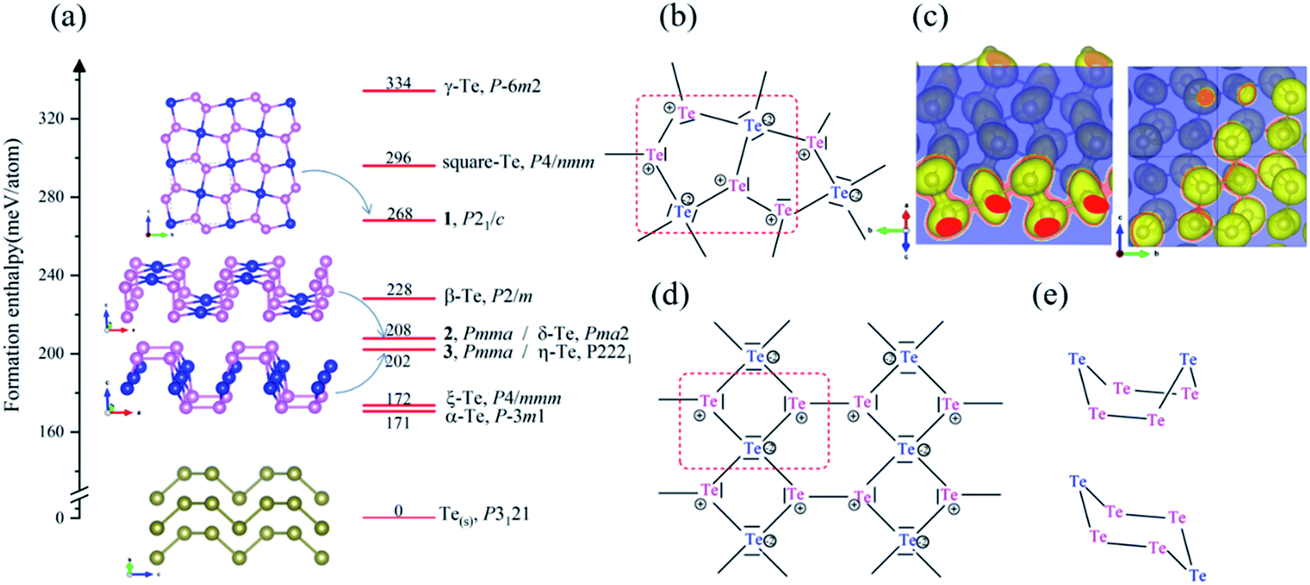 | ||
Fig. 2 (a) The formation enthalpies and structure motifs of 2D Te nets, 1, 2 and 3; (b) A resonant Lewis structure for repeat unit (red dashed) in 2D Te net 1, containing AX3E pyramidal (pink) and AX4E2 square planar (blue) Te units (VSEPR notations); (c) isosurface of ELF contours of 2D Te net 1 in (1 0 1) and (![[8 with combining macron]](https://www.rsc.org/images/entities/char_0038_0304.gif) ![[2 with combining macron]](https://www.rsc.org/images/entities/char_0032_0304.gif) 1) plane with the isovalue of 0.75; (d) topology pattern in 2D Te nets 2 and 3; (e) conformational 6-ring Te6: boat and chair motifs in 2D Te nets 2 and 3. In (a), the enthalpy of bulk ground-state P3121 Te phase is taken as the energy reference. Formal charges are circled in (b) and (d). 1) plane with the isovalue of 0.75; (d) topology pattern in 2D Te nets 2 and 3; (e) conformational 6-ring Te6: boat and chair motifs in 2D Te nets 2 and 3. In (a), the enthalpy of bulk ground-state P3121 Te phase is taken as the energy reference. Formal charges are circled in (b) and (d). | ||
In the following, we will first examine the viability of three 2D nets and then try to understand the covalent topologies in three 2D Te crystal structures by discussing their structural and bonding properties,74 followed by exploring their bulk counterparts through vertically packing the 2D Te nets. Next, the electronic structures, optical absorption, the carrier mobility, and band alignment in those three 2D Te crystal structures were studied in detail.
2D Te net 1 belongs to the monoclinic space group P21/c (SG 14, Z = 6). The lattice of 2D Te net 1 is composed of fused and strained non-planar five-membered rings, which may explain its relatively high formation enthalpy. Two symmetric sites for Te atoms can be identified in 2D Te net 1, one square planar and two pyramidal chemical motifs per repeat unit. The structure topology of 2D Te net 1 can be easily rationalized using simple electron count and VSEPR rules. A resonant Lewis structure of 2D Te net 1 is depicted in Fig. 2(b). In 2D Te net 1, the four-coordinated Te atom is surrounded by six electrons pairs, including four bonding and two non-bonding (AX4E2), and then exhibits a square-planar environment, while each three-coordinated Te atom follows the octet rule and thus a pyramidal environment is expected (AX3E center). The Te(AX4E2)–Te(AX3E) bond lengths of 3.03 Å are significantly longer than that of Te(AX3E)–Te(AX3E) distance of 2.75 Å because of the lone pairs congestion around Te centres.
To accurately understand the electron distribution and bonding character in 2D Te net 1, the Bader charge and ELF analysis were further investigated in the following study. The Bader charge analysis shows that each three-coordinated Te atom accepts 0.05 e from one four-coordinated Te atom, thus the formal charge of four-coordinated Te atom is +0.10 |e|. Obviously, the above discussed VSEPR rules overestimate the charge transfer between Te atoms in different symmetric sites. In Fig. 2(c), due to a shared accumulated electron distribution in ELF contours, the covalent Te–Te bonds between pyramidal TeTe3 centers (2.75 Å) are found, and the corresponding bond order is computed as 0.93, which is stronger than that (0.78 for 2.89 Å) in the bulk P3121 Te. In the planar TeTe4 units, relatively weaker covalent Te–Te bonds (3.04 Å and 3.05 Å) are indicated in the ELF contour, in line with the bond order of 0.64 and 0.65.
Another two 2D tellurium phases present these specific local structural environments found in 2D Te net 1, namely 2D Te net 2 (Pmma, SG 51, Z = 6) and 2D Te net 3 (Pmma, SG 51, Z = 6) (see Fig. 2). These two phases (η-Te and δ-Te) have been proposed by Liu and coauthors,42 but the authors did not discuss the bonding of 2D Te nets 2 and 3, neither rationalized the encountered structural features; therefore, in the following, we propose to discuss the bonding in 2D Te nets 2 and 3, which present similar building blocks but different association to 2D Te net 1.
First, the Te–Te distances in 2D Te net 2 and 3 fall into 2.76–3.02 Å and can be safely assigned to single bonds (2.89 Å in bulk polymeric P3121 Te). In their 2D covalent nets, one may see one-dimensional Te3 ribbons running along a axis. The repeated Te3 unit of the chain is depicted in Fig. 2(d). Note that such 1D X3 ribbons were also encountered in intermetallic phases, such as β-ZrSb2.77 These 1D Te3 ribbons of vertex-sharing Te squares are linked through single Te–Te bonds, thus 4- and non-planar 6-rings are observed in the corrugated Te nets of 2D Te nets 2 and 3. Two different conformational structures of the single bonded Te6 ring are observed in Fig. 2(e), namely boat conformation in 2D Te net 2, and armchair in 2D Te net 3.
The understanding of the local structural environment follows the one presented in our bonding discussion of 2D Te net 1. The Te–Te non-bonding separations between 3-coordinated atoms along a direction were calculated to be 4.20 Å and 5.17 Å in 2D Te nets 2 and 3, respectively. Therefore, the Te lone pairs repulsions are stronger in 2D Te net 2 (see its Lewis structure in Fig. 2(d)). Following organic chemistry rules, e.g., cyclohexane C6H6, the chair conformation is the most stable conformation of a single bonded 6-ring, and the second, slightly but significantly less stable conformer is the boat conformation. To conclude, these structural conformation and electronic configuration explain the energy ordering of 2D Te net 2 and 3 (2D Te net 2 is located at 6 meV per atom, i.e., ∼0.6 kJ mol−1, above 2D Te net 3). We will evocate this feature when looking at the packing of Te slabs in crystalline bulk crystal in the following section.
3.3 From 2D nets to bulk layered materials
Three bulk Te crystal structures of 1_bulk (C2/c, SG 15, Z = 12), 2_bulk (Cmmm, SG 65, Z = 6), and 3_bulk (Pnma, SG 62, Z = 12) were constructed and investigated through extensive structural optimizations of different 2D layer packing and the corresponding crystal structures are depicted in Fig. 3(a)–(c). Stationary points were found, and all proposed bulk crystals are local minima on the PES. Their phonon dispersion curves are given in Fig. S9.† Besides, the calculated enthalpies and structural parameters of those bulk Te allotropes are listed in Tables S6 and S7.†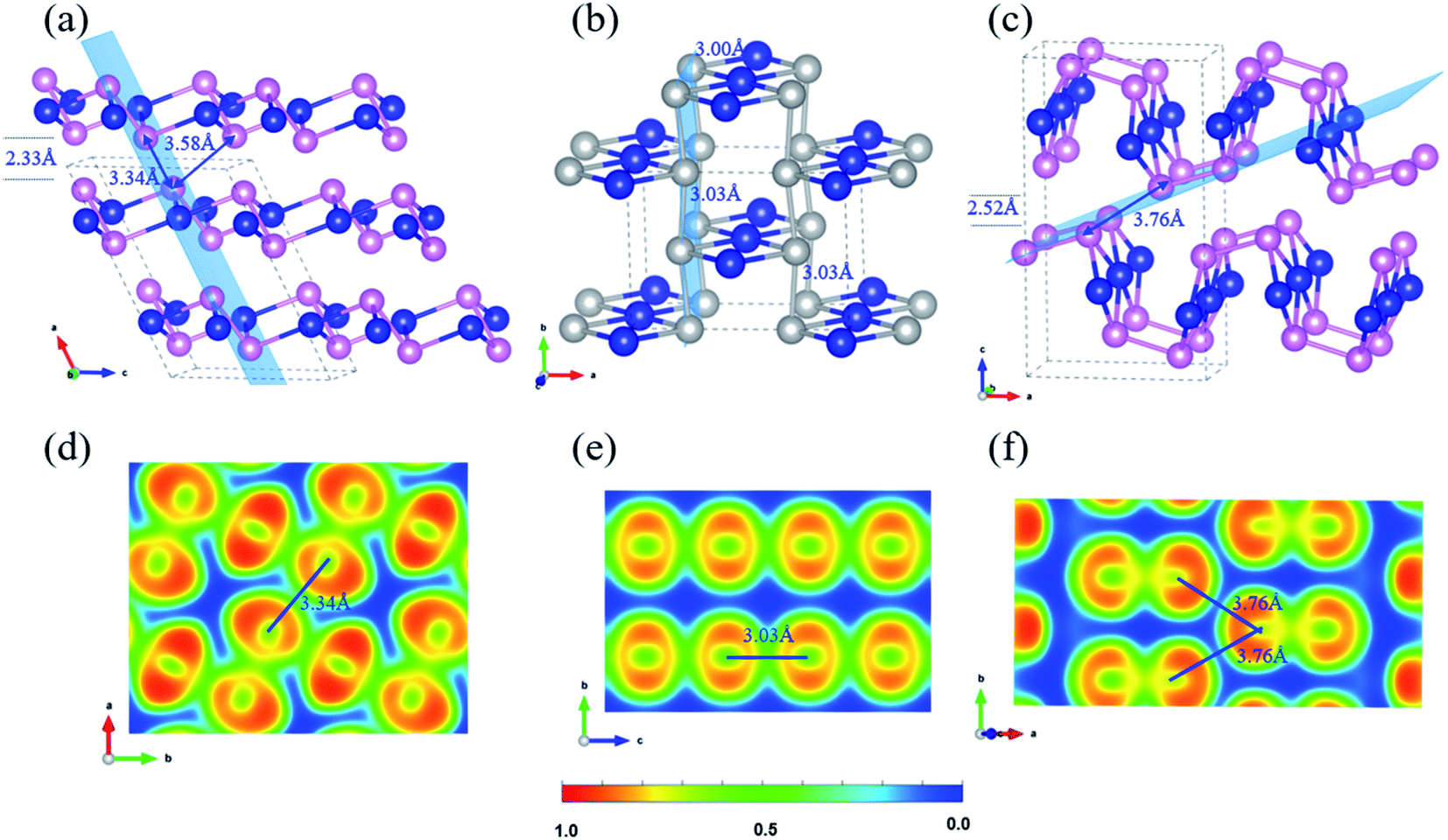 | ||
Fig. 3 Side view of bulk layered Te: (a) 1_bulk, (b) 2_bulk, and (c) 3_bulk; 2D isosurface of ELF contours for (d) 1_bulk 2 × 2 (100) plane, (e) 2_bulk 1 × 2 (001) plane and (f) 3_bulk 1 × 2 (![[1 with combining macron]](https://www.rsc.org/images/entities/char_0031_0304.gif) 14) plane. In (a–c), silver balls indicate the seesaw TeTe4 centres, and the blue, pink colours are as the same as that in Fig. 1. The specific light blue planes depicted in (a–c) indicate the ELF contours in (d–f). 14) plane. In (a–c), silver balls indicate the seesaw TeTe4 centres, and the blue, pink colours are as the same as that in Fig. 1. The specific light blue planes depicted in (a–c) indicate the ELF contours in (d–f). | ||
1_bulk lies at 0.102 eV per atom above the ground-state phase P3121 Te and presents an AB stacking with a vdW separation of 2.33 Å. It crystallizes in the monoclinic space group C2/c. Within the slab, Te–Te bond lengths are in the range of 2.88–3.05 Å with calculated bond order of 0.57–0.75, analog to 2D Te net 1. Long Te–Te separations of 3.34 Å and 3.58 Å are computed between pyramidal Te centers of two adjacent layers, reflecting similar bonding character of interchain spacing of 3.40 Å in stable polymeric P3121 Te structure. To clarify the bonding nature of Te–Te contacts between neighboring layers in C2/c Te phase, 2D ELF isosurface contours were plotted in Fig. 3(d). It shows that the Te–Te bond (3.34 Å) between the neighboring layers possesses a mixture of covalent and metallic characters and the bond order was computed as 0.32, which is close to that of the long Te–Te bond (3.40 Å) in P3121 Te structure. Similar bonding character of Te–Te contact (3.58 Å) with bond order of 0.23 is found in the ELF contour along the (2 0 −1) plane shown in Fig. S10 (ESI).† What is more, to further assess the Te–Te bonding strength in 1_bulk, COHP curves and -ICOHP were further computed. In Fig. S11,† COHP curve shows that the Te–Te bonding between two adjacent layers is much weaker than that within the slab. This bonding anisotropy is also reflected by −ICOHP values, i.e., 0.63 eV per bond for long Te–Te bond (3.34 Å), 1.51–2.31 eV per bond for Te–Te bonds (2.88–3.05 Å).
The crystal search of 2_bulk did not lead to a layered material, instead to a 3D covalent net with the formation enthalpy of 0.053 eV per atom, as displayed in Fig. 3(b). Through an AA stacking, two slabs become linked into 2_bulk through Te–Te bonds of 3.03 Å. Then four-coordinated seesaw Te centers appear, stabilizing the system through delocalized bonding. The Te–Te contacts (3.03 Å) between two slabs can be verified to be covalent and metallic bonding in 2D ELF isosurface contour shown in Fig. 2(e). Additionally, the bond order of those bonds calculated in Chargemol program is 0.53. Therefore, 2_bulk does not fall into the lamellar material family. This electronic reorganization somehow illustrates the reactivity of the proposed 2D Te net 2, which would unlikely exist as an isolated 2D material.
3_bulk has an orthorhombic space group Pnma with two layers per unit cell with a vacuum spacing of 2.52 Å and the nearest Te–Te distance between two adjoint layers is 3.76 Å as shown in Fig. 3(c). A slightly distorted covalent slab can be observed as well as long Te–Te contacts between layers (3.76 Å). ELF contours in Fig. 3(f) show that covalent Te–Te bonding (2.84 Å) within the slab with the bond order of 0.82, and there is no chemical bond along the Te–Te contact (3.76 Å, bond order of 0.15), which indicates the vdW interaction between the adjacent layers. The exfoliation energy of 2D Te net 3 from 3_bulk was calculated as 144 meV per atom. These bulk phases have close formation enthalpies 57 meV per atom in 3_bulk vs. 53 meV per atom in 2_bulk, even their bonding topologies are quite different.
3.4 Electronic properties and optical properties
Upon the confirmation of the viability of 2D Te, the electronic properties of the three 2D Te structures were investigated carefully. In the previous work, band gaps of 2D Te nets 1, 2 and 3 were evaluated using PBE.45 It is however known that PBE tends to underestimate these gaps, thus, here HSE06 functional was employed, owing to its better performances (despite a larger computational cost). The band structures of 2D Te phases calculated at the HSE06 level of theory are depicted in Fig. 4.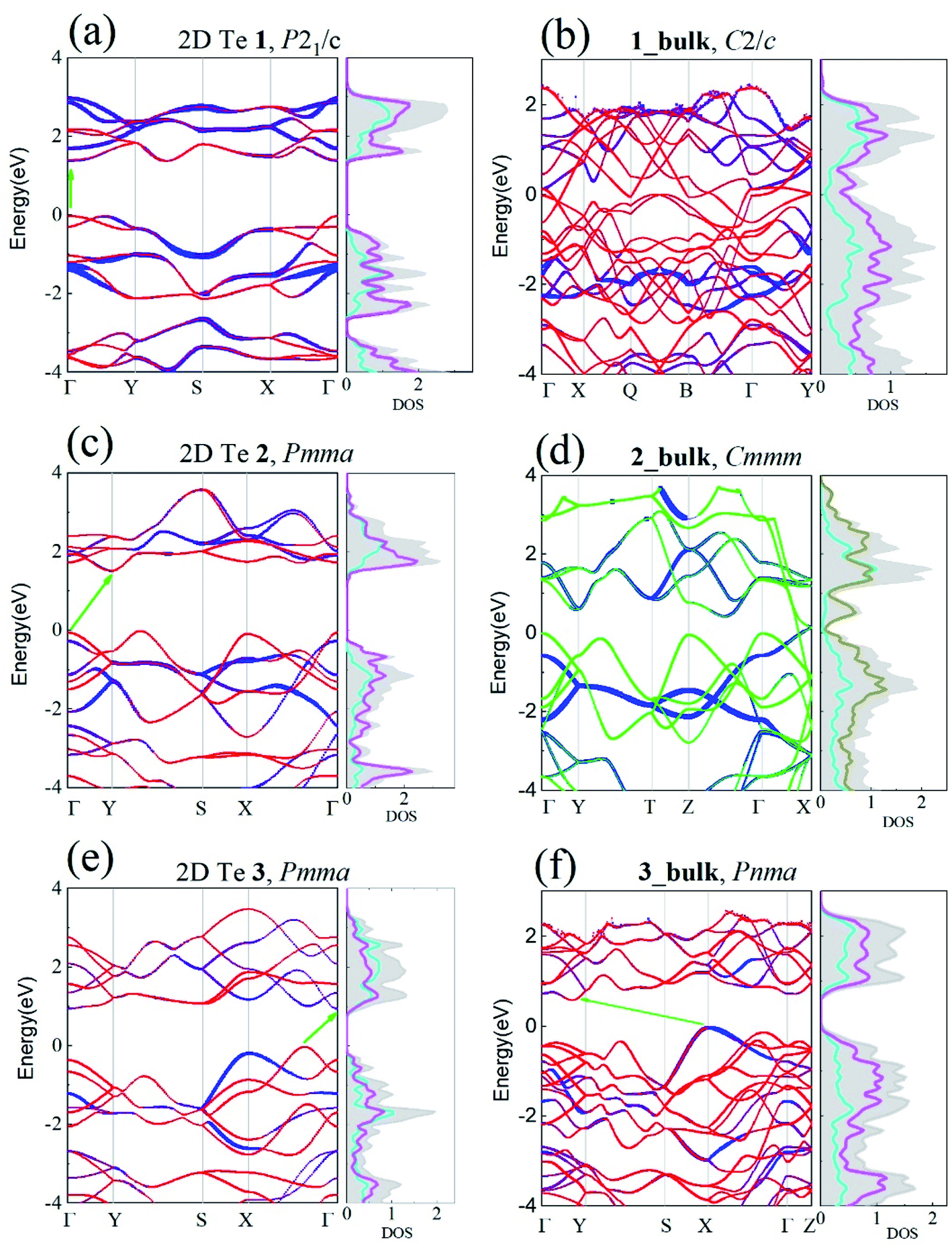 | ||
| Fig. 4 Electronic projected band structures and DOS of 2D and bulk Te structures within the HSE06 theoretical level: (a) 2D Te net 1, (b) 1_bulk, (c) 2D Te net 2, (d) 2_bulk, (e) 2D Te net 3, and (f) 3_bulk. The Fermi energy is set to zero. In (a–f), the blue, red and green colours indicate the atomic contributions of planar TeTe4 centre, pyramidal TeTe3 centre and seesaw TeTe4 centre. The cyan, magenta, and dark yellow lines in DOS are for the 5p orbital of planar TeTe4 centre, pyramidal TeTe3 centre and seesaw TeTe4 centre, respectively. In the DOS panel, the grey shadow is for the total DOS. | ||
One can see that the band gaps of those three 2D Te structures are enlarged compared with the bulk P3121 Te. Among those three 2D Te nets, 1 is a direct semiconductor at the high symmetric k-point Γ with band gap of 1.388 eV, while 2 have a larger indirect band gap of 1.512 eV and its minimum direct band gap at the high symmetric k-point Γ is 1.848 eV. It is noteworthy that 2D Te net 3 possesses an indirect band gap of 0.951 eV (Fig. 4(e)), but the direct transition from VBM to conduction band edge is only 0.030 eV higher than the indirect gap, because of the multi-valleys in the flat conduction band edge in 2D Te net 3. This intriguing direct band transition will no doubt significantly promote the low efficiency of indirect transition and improve the optical absorption for optoelectronic applications.78 Additionally, it can be also found from projected DOS in Fig. 4 that, in 2D Te nets 1, 2 and 3, the VBM is mainly composed of the 5p orbitals from three-coordinated Te atoms (TeTe3 centres), while 5p orbitals from four-coordinated Te atoms (TeTe4 centres) make important contributions to the CBM. The partial charge densities of VBM and CBM presented in Fig. S12–S14† proved the 5p orbital distributions in 2D Te nets.
Besides, the electronic band structures of corresponding Te bulk materials were also investigated at the HSE06 level of theory. Our calculation shows that 1_bulk and 2_bulk are metallic, and their DOS and partial charge distribution (Fig. S15 in ESI†) indicate that the energy states near Fermi energy are dominated by 5p orbitals of the seesaw TeTe4 centres. The van der Waals layered crystal, 3_bulk is an indirect semiconductor, and its band gap is 0.731 eV, which is smaller than that of its 2D counterpart as expected. Its band structure and DOS are depicted in Fig. 4(f).
Note that the band gaps of 2D Te nets 1, 2, and 3 are in the optimal band gap range (1.0–1.8 eV) as photovoltaic absorber materials.79,80 Specially, the direct band gap of 2D Te net 1 (1.388 eV) is quite close the optimum semiconductor band gap (1.34 eV) which will lead to a maximum photovoltaic energy conversion efficiency (33.7%) for a single-junction solar cell.81
Additionally, the direct and pseudo-direct band structures character in 2D Te nets 1 and 3 will promote the optical absorptions and thus their optical absorptions as a function of photon energy along different spatial directions were investigated and shown in Fig. S16 in ESI.† It shows that those semiconducting 2D Te structures exhibit strong and prominent optical absorptions in the range of 1.5–4 eV for the light polarization along in-plane directions, which covers the visible to ultraviolet light regime. Therefore, the strong and broad optical absorption in the visible regime indicates the possibility of 2D Te structures of being excellent candidates for solar energy conversion.
To summarize, the wide-ranged electronic properties, from metallic to semiconducting characters, were found in one-, two- and three-dimensional covalent Te phases. Three 2D Te allotropes 1, 2, and 3 possess moderate band gaps (0.951–1.512 eV), because of the strong covalent bonding and electron localization in their Te nets. Due to the quantum size effect, the parental bulk crystal of 2D 3 obtained by vertically packing 2D 3 Te nets has a slightly lower band gap than 2D 3 (from 0.951 to 0.731 eV, respectively). In addition, the weak covalent bonding between the neighbouring Te chains in bulk polymeric P3121 Te produces a small band gap (0.326 eV) by increasing the coordination number of Te from 3 to 6, i.e., higher is the averaged coordination number, stronger is the density delocalization over the Te net, thus lower is the energy gap. Moreover, in 1_bulk and 2_bulk, higher coordination number of Te is observed (see Table S8 in ESI†); this leads to a stronger delocalized density and both bulk Te allotropes are metallic. Our crystal structure search reveals the diverse physical and electronic properties of Te allotropes, determined by the rich chemistry of Te element.
3.5 Transport properties
Here, we investigated the transport properties of those three 2D Te phases for potential applications in optoelectronic and solar cell devices. The calculated effective mass and mobility of carriers are listed in Table 1. Although PBE calculations always underestimate the band gap values in semiconductors, PBE can predict correct curvatures of valence and conduction bands and the calculated carrier mobilities using PBE are in good agreement with the experiments in numerous 2D crystals.82| 2D Te | Carrier type |
|
|
El-x | El-y | C2D-x | C2D-y | μx | μy |
|---|---|---|---|---|---|---|---|---|---|
| 1 | e | 2.274 | 0.404 | 2.402 | 3.135 | 16.271 | 12.588 | 27.758 | 70.665 |
| h | 1.171 | 0.163 | 3.290 | 1.569 | 16.271 | 12.588 | 62.705 | 1523.962 | |
| 2 | e | 0.371 | 0.195 | 3.685 | 6.591 | 6.327 | 41.198 | 367.362 | 386.088 |
| h | 0.378 | 0.195 | 1.577 | 6.384 | 6.327 | 41.198 | 1026.237 | 407.739 | |
| 3 | e | 1.011 | 0.145 | 1.255 | 2.291 | 6.681 | 18.986 | 233.802 | 1390.817 |
| h | 0.505 | 0.195 | 2.325 | 3.785 | 6.681 | 18.986 | 166.517 | 462.439 |
Regarding transport properties, the calculated effective masses along the directions of x (a) and y (b) lattice vectors indicate an anisotropic transport feature. 2D Te nets 1 and 3 possess heavier electrons than holes, which can be revealed by the greater curvature of valence band edge in their band structures shown in Fig. 4. In particular, the calculated electron effective mass of 2D Te net 2 is close to that of arsenene and antimonene monolayers with the value of 0.20–0.29 m0.83 However, the calculated electron effective mass of predicted 2D Te structures in the present work are larger than that in α-Te.42
VBM, CBM and total energy of 2D Te structures as a function of the lattice dilation along x and y directions in the range of ±0.01% were calculated. The deformation potential El can be obtained through linearly fitting the band edge energy shift with respect to the vacuum level under slight strain along x and y directions. The calculated results suggest that the responses of CBM and VBM to the external strain are also anisotropic along different transport directions. It can be observed that the elastic moduli of 2D Te structures are smaller than those of graphene (328.02/328.30 J m−2), silicene (85.48/85.99 J m−2) and black phosphorene (28.94/101.60 J m−2).84,85 This suggests a pronounced weakness of those 2D structures in resistance to deformation under biaxial stress conditions. Due to small effective mass and moderate deformation potential constants, the predicted carrier mobilities in 2D Te nets along in-plane direction can reach a level of beyond 1 × 103 cm2 V−1 s−1, which is comparable with that of black phosphorene (1.10–1.14 × 103 cm2 V−1 s−1).85 Interestingly, anisotropic transport properties between the electrons and holes will be beneficial to suppress the recombination of electron–hole pairs, consequently, to enhance the performance of photofunctional devices.86
3.6 Potential for photochemical water splitting
The band alignments between different semiconductors are the driving force for the transportation of ionic and electronic charge carriers in electronic and optoelectronic devices. Therefore, the absolute band energy positions were evaluated by computing the ionization potentials of the proposed 2D Te structures with the vacuum potential as reference energy. Their band-edge potentials are displayed in Fig. 5 in comparison with that of bulk silicon and 2D black phosphorene. Firstly, it can be found that structure diversity in 2D Te nets result in wide variation of band edge positions, especially on the CBMs. Thus, it provides a possibility to construct vdW heterostructures with various 2D nanomaterials for different functional band alignments. Remarkably, type-II band alignments can be constructed between black phosphorene and 2D Te allotropes with the conduction band offset (CBO) of 0.19–0.52 eV, and 0.53–0.74 eV for the valence band offset (VBO), because the calculated energy edge positions of 2D Te structures are higher than that of 2D black phosphorene.87 Similarly, the type-II band alignment can be also obtained between 2D Te nets and Si bulk with CBO (VBO) of 0.24–0.66 eV (0.27–0.48 eV). The staggered band alignment will lead to localization of electrons and holes in different layers during photoexcitation and then enhance the spatial separation of excitons before recombination.88 Therefore, 2D Te/black phosphorene or 2D Te/Si bulk heterostructures can be promising for harnessing long-lived excitons in efficient light-harvesting devices. Secondly, Fig. 5 depicts CBM and VBM energy levels with the redox potentials of water splitting. Results show that the CBM energy level of all semiconducting 2D Te nets 1, 2 and 3 are higher than the reduction potential of H+/H2 (4.44 eV), while their VBM are located above the O2/H2O oxidation potential (5.67 eV), which suggests that all predicted 2D Te structures cannot be promising candidate semiconductors for overall photo-catalytic water splitting. Lastly, we found that the calculated VBM energy levels (−4.69 to −4.90 eV) of 2D Te structures are close to the reported Fermi energies of well-known electrode materials (Pt: −5.12 to −5.93, Pd: −5.22 to −5.60, Au: −5.10 to −5.47, Ni: −5.04 to −5.35, Co: −5 eV),89 which indicates a low Schottky barrier for more efficient hole injection through the contact than electron.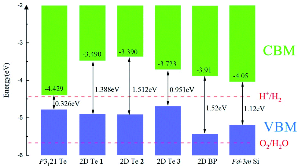 | ||
| Fig. 5 The band alignment of bulk P3121 Te phase, three predicted 2D Te structures and black phosphorene (BP),87 and bulk Fdm silicon phase.90 The vacuum level is set as reference and the VBM and CBM are indicated in blue and grey. Band gaps of bulk, 2D Te phases, 2D BP and bulk Fdm Si are marked. | ||
4. Conclusion
A first-principles crystal prediction calculation on 2D Te covalent allotropes was performed to provide a new insight into structural richness and potential photofunctional applications of group VI 2D-Xenes. The mixture of pyramidal 3-coordinated TeTe3 centres (AX3E) and planar 4-coordinated TeTe4 centres (AX4E2) could be explained by simple electron count and VSEPR rules. Furthermore, the strong stabilities of these 2D structures are confirmed and electronic property calculations show that, all three semiconducting 2D Te structures possess significant band gaps in the range of 0.951–1.512 eV. Moreover, the investigation of transport properties in 2D Te structures reveals that the small electron effective mass and deformation potential constants in 2D Te phases can lead to a high carrier mobility of ∼1.5 × 103 cm2 V−1 s−1. The present work also shows that the wide tunability in energy positions of CBM and VBM will provides a practical way to construct different heterostructures by combining 2D Te phases and other 2D nanomaterials or bulk materials. Lastly, by vertically packing those 2D Te nets, three new Te bulk layered structures are proposed including two covalent crystals and one van der Waals layered crystal. Our work comprehensively investigated the bonding and electronic properties in 2D group VI elemental nanostructures and will further stimulate exploration in related materials synthesis.Conflicts of interest
There is no conflict of the interest among the authors.Acknowledgements
This work is supported by National Natural Science Foundation of China (Grants No. 51872242, 52111530033 and 51761135032), Foreign Talents Introduction and Academic Exchange Program of China (No. B08040), the Fundamental Research Funds for the Central Universities (No. 3102019MS0405, D5000200142), and the ANR PRCI French-Chinese Predict_2D_Nanomat (P.I. G.F. and K.S.), the FEDER and Nouvelle Aquitaine Region (France). Junjie Wang, Heng Zhang and Gilles Frapper also thank PHC Cai Yuanpei 2019 China-France program (China Scholarship Council and Ministère de l'Europe et des Affaires étrangères – french ambassy, Beijing) for the financial support. We acknowledge the High-Performance Computing Centre of MSEA (MSEA International Institute for Materials Genome, China) and NWPU (Northwestern Polytechnical University, China), the High-Performance Computing Centres of Poitiers University (Mesocentre SPIN, France) and Jean Zay/IDRIS – TGCC/Curie GENCI (France) under Project No. A0100807539 for allocation of computing time.References
- K. S. Novoselov, A. K. Geim, S. V. Morozov, D. Jiang, M. I. Katsnelson, I. Grigorieva, S. Dubonos and A. A. Firsov, Nature, 2005, 438, 197–200 CrossRef CAS PubMed.
- Y. Zhu, S. Murali, W. Cai, X. Li, J. W. Suk, J. R. Potts and R. S. Ruoff, Adv. Mater., 2010, 22, 3906–3924 CrossRef CAS PubMed.
- A. Molle, J. Goldberger, M. Houssa, Y. Xu, S.-C. Zhang and D. Akinwande, Nat. Mater., 2017, 16, 163–169 CrossRef CAS PubMed.
- Z. Tian, K. Chen, S. Sun, J. Zhang and W. Cui, J. Adv. Ceram., 2019, 8, 72–78 CrossRef CAS.
- C. Tan, X. Cao, X.-J. Wu, Q. He, J. Yang, X. Zhang, J. Chen, W. Zhao, S. Han and G.-H. Nam, Chem. Rev., 2017, 117, 6225–6331 CrossRef CAS PubMed.
- J. Zhou, J. Lin, X. Huang, Y. Zhou, Y. Chen, J. Xia, H. Wang, Y. Xie, H. Yu and J. A. Lei, Nature, 2018, 556, 355–359 CrossRef CAS PubMed.
- M. Naguib, M. Kurtoglu, V. Presser, J. Lu, J. Niu, M. Heon, L. Hultman, Y. Gogotsi and M. W. Barsoum, Adv. Mater., 2011, 23, 4248–4253 CrossRef CAS PubMed.
- S. Wang, N. Miao, K. Su, V. A. Blatov and J. Wang, Nanoscale, 2021, 13, 8254–8263 RSC.
- M. Wu, Y. He, L. Wang, Q. Xia and A. Zhou, J. Adv. Ceram., 2020, 9, 749–758 CrossRef CAS.
- A. Jain, S. P. Ong, G. Hautier, W. Chen, W. D. Richards, S. Dacek, S. Cholia, D. Gunter, D. Skinner and G. Ceder, APL Mater., 2013, 1, 011002 CrossRef.
- S. Curtarolo, G. L. Hart, M. B. Nardelli, N. Mingo, S. Sanvito and O. Levy, Nat. Mater., 2013, 12, 191–201 CrossRef CAS PubMed.
- H. Yin, X. Shi, C. He, M. Martinez-Canales, J. Li, C. J. Pickard, C. Tang, T. Ouyang, C. Zhang and J. Zhong, Phys. Rev. B, 2019, 99, 041405 CrossRef CAS.
- S. Haastrup, M. Strange, M. Pandey, T. Deilmann, P. S. Schmidt, N. F. Hinsche, M. N. Gjerding, D. Torelli, P. M. Larsen and A. C. Riis-Jensen, 2D Mater., 2018, 5, 042002 CrossRef CAS.
- N. Mounet, M. Gibertini, P. Schwaller, D. Campi, A. Merkys, A. Marrazzo, T. Sohier, I. E. Castelli, A. Cepellotti and G. Pizzi, Nat. Nanotechnol., 2018, 13, 246–252 CrossRef CAS PubMed.
- N. R. Glavin, R. Rao, V. Varshney, E. Bianco, A. Apte, A. Roy, E. Ringe and P. M. Ajayan, Adv. Mater., 2020, 32, 1904302 CrossRef CAS PubMed.
- F. Su, X. Hou, J. Qin and Z. S. Wu, Batteries Supercaps, 2020, 3, 10–29 CrossRef CAS.
- Y. Song, E. M. D. Siriwardane, Y. Zhao and J. Hu, ACS Appl. Mater. Interfaces, 2021 DOI:10.1021/acsami.1c01044.
- J. Qi, S. Wang, J. Wang, N. Umezawa, V. A. Blatov and H. Hosono, J. Phys. Chem. Lett., 2021, 12, 4823–4832 CrossRef CAS PubMed.
- D. Royer and E. Dieulesaint, J. Appl. Phys., 1979, 50, 4042–4045 CrossRef CAS.
- S. Lin, W. Li, Z. Chen, J. Shen, B. Ge and Y. Pei, Nat. Commun., 2016, 7, 1–6 Search PubMed.
- L. A. Ba, M. Döring, V. Jamier and C. Jacob, Org. Biomol. Chem., 2010, 8, 4203–4216 RSC.
- Y. Liu, S. Hu, R. Caputo, K. Sun, Y. Li, G. Zhao and W. Ren, RSC Adv., 2018, 8, 39650–39656 RSC.
- C. Soulard, X. Rocquefelte, M. Evain, S. Jobic, H.-J. Koo and M.-H. Whangbo, J. Solid State Chem., 2004, 177, 4724–4731 CrossRef CAS.
- H.-G. Junginger, Solid State Commun., 1967, 5, 509–511 CrossRef CAS.
- S. Kabalkina, L. Vereshchagin and B. Shulenin, Sov. Phys. JETP, 1964, 18, 1422–1423 Search PubMed.
- K. Aoki, O. Shimomura and S. Minomura, J. Phys. Soc. Jpn., 1980, 48, 551–556 CrossRef CAS.
- J. Jamieson and D. McWhan, J. Chem. Phys., 1965, 43, 1149–1152 CrossRef CAS.
- G. Parthasarathy and W. Holzapfel, Phys. Rev. B: Condens. Matter Mater. Phys., 1988, 37, 8499 CrossRef CAS PubMed.
- Z. Tang, Y. Wang, K. Sun and N. A. Kotov, Adv. Mater., 2005, 17, 358–363 CrossRef CAS.
- M. Mo, J. Zeng, X. Liu, W. Yu, S. Zhang and Y. Qian, Adv. Mater., 2002, 14, 1658–1662 CrossRef CAS.
- L. Wu, W. Huang, Y. Wang, J. Zhao, D. Ma, Y. Xiang, J. Li, J. S. Ponraj, S. C. Dhanabalan and H. Zhang, Adv. Funct. Mater., 2019, 29, 1806346 CrossRef.
- X. Huang, J. Guan, Z. Lin, B. Liu, S. Xing, W. Wang and J. Guo, Nano Lett., 2017, 17, 4619–4623 CrossRef CAS PubMed.
- Y. Wang, G. Qiu, R. Wang, S. Huang, Q. Wang, Y. Liu, Y. Du, W. A. Goddard, M. J. Kim and X. Xu, Nat. Electron., 2018, 1, 228–236 CrossRef.
- M. Amani, C. Tan, G. Zhang, C. Zhao, J. Bullock, X. Song, H. Kim, V. R. Shrestha, Y. Gao and K. B. Crozier, ACS Nano, 2018, 12, 7253–7263 CrossRef CAS PubMed.
- G. Qiu, S. Huang, M. Segovia, P. K. Venuthurumilli, Y. Wang, W. Wu, X. Xu and P. D. Ye, Nano Lett., 2019, 19, 1955–1962 CrossRef CAS PubMed.
- J. Peng, Y. Pan, Z. Yu, J. Wu, J. Wu, Y. Zhou, Y. Guo, X. Wu, C. Wu and Y. Xie, Angew. Chem., Int. Ed., 2018, 57, 13533–13537 CrossRef CAS PubMed.
- L. Xian, A. P. Paz, E. Bianco, P. M. Ajayan and A. S. Rubio, 2D Mater., 2017, 4, 041003 CrossRef.
- J. Qiao, Y. Pan, F. Yang, C. Wang, Y. Chai and W. Ji, Sci. Bull., 2018, 63, 159–168 CrossRef CAS.
- Y. Xiang, S. Gao, R.-G. Xu, W. Wu and Y. Leng, Nano Energy, 2019, 58, 202–210 CrossRef CAS.
- C. Yan, C. Wang, L. Zhou, P. Guo, K. Liu, Z.-Y. Lu, Z. Cheng, Y. Chai, A. Pan and W. Ji, Chin. Phys. B, 2020, 29, 097103 CrossRef CAS.
- D. Liu, X. Lin and D. Tománek, Nano Lett., 2018, 18, 4908–4913 CrossRef CAS PubMed.
- Z. Zhu, X. Cai, S. Yi, J. Chen, Y. Dai, C. Niu, Z. Guo, M. Xie, F. Liu and J.-H. Cho, Phys. Rev. Lett., 2017, 119, 106101 CrossRef PubMed.
- S. Khatun, A. Banerjee and A. J. Pal, Nanoscale, 2019, 11, 3591–3598 RSC.
- J. Chen, Y. Dai, Y. Ma, X. Dai, W. Ho and M. Xie, Nanoscale, 2017, 9, 15945–15948 RSC.
- C. Zhao, X. Cai, L. Liu, C. Liu, Z. Zeng, C. Niu, C. Xia and Y. Jia, Adv. Theory Simul., 2021, 4, 2000265 CrossRef CAS.
- A. R. Oganov and C. W. Glass, J. Chem. Phys., 2006, 124, 244704 CrossRef PubMed.
- A. R. Oganov, A. O. Lyakhov and M. Valle, Acc. Chem. Res., 2011, 44, 227–237 CrossRef CAS PubMed.
- A. O. Lyakhov, A. R. Oganov, H. T. Stokes and Q. Zhu, Comput. Phys. Commun., 2013, 184, 1172–1182 CrossRef CAS.
- Z. Wang, X.-F. Zhou, X. Zhang, Q. Zhu, H. Dong, M. Zhao and A. R. Oganov, Nano Lett., 2015, 15, 6182–6186 CrossRef CAS PubMed.
- X.-F. Zhou, X. Dong, A. R. Oganov, Q. Zhu, Y. Tiann and H.-T. Wang, Phys. Rev. Lett., 2014, 112, 085502 CrossRef.
- G. Kresse and J. Furthmüller, Comput. Mater. Sci., 1996, 6, 15–50 CrossRef CAS.
- G. Kresse and J. Furthmüller, Phys. Rev. B: Condens. Matter Mater. Phys., 1996, 54, 11169 CrossRef CAS PubMed.
- J. P. Perdew, K. Burke and M. Ernzerhof, Phys. Rev. Lett., 1996, 77, 3865 CrossRef CAS PubMed.
- S. Grimme, J. Comput. Chem., 2006, 27, 1787–1799 CrossRef CAS PubMed.
- H. J. Monkhorst and J. D. Pack, Phys. Rev. B: Solid State, 1976, 13, 5188 CrossRef.
- J. Heyd, G. E. Scuseria and M. Ernzerhof, J. Chem. Phys., 2003, 118, 8207–8215 CrossRef CAS.
- A. Togo, F. Oba and I. Tanaka, Phys. Rev. B: Condens. Matter Mater. Phys., 2008, 78, 134106 CrossRef.
- T. A. Manz and D. S. Sholl, J. Chem. Theory Comput., 2011, 7, 4146–4164 CrossRef CAS PubMed.
- T. A. Manz and N. G. Limas, RSC Adv., 2016, 6, 47771–47801 RSC.
- T. A. Manz, RSC Adv., 2017, 7, 45552–45581 RSC.
- N. G. Limas and T. A. Manz, RSC Adv., 2018, 8, 2678–2707 RSC.
- S. Maintz, V. L. Deringer, A. L. Tchougréeff and R. Dronskowski, J. Comput. Chem., 2016, 37, 1030–1035 CrossRef CAS PubMed.
- S. Maintz, V. L. Deringer, A. L. Tchougréeff and R. Dronskowski, J. Comput. Chem., 2013, 34, 2557–2567 CrossRef CAS PubMed.
- E. Sanville, S. D. Kenny, R. Smith and G. Henkelman, J. Comput. Chem., 2007, 28, 899–908 CrossRef CAS PubMed.
- A. Savin, R. Nesper, S. Wengert and T. F. Fässler, Angew. Chem., Int. Ed., 1997, 36, 1808–1832 CrossRef CAS.
- K. Momma and F. Izumi, J. Appl. Crystallogr., 2011, 44, 1272–1276 CrossRef CAS.
- J. Bardeen and W. Shockley, Phys. Rev., 1950, 80, 72 CrossRef CAS.
- Y. Xu, H. Zhang, H. Shao, G. Ni, J. Li, H. Lu, R. Zhang, B. Peng, Y. Zhu and H. Zhu, Phys. Rev. B, 2017, 96, 245421 CrossRef.
- S. Yi, Z. Zhu, X. Cai, Y. Jia and J.-H. Cho, Inorg. Chem., 2018, 57, 5083–5088 CrossRef CAS PubMed.
- J. K. Burdett, Chemical bonds: a dialog, John Wiley & Sons, 1997, vol. 13 Search PubMed.
- H. Peng, N. Kioussis and G. J. Snyder, Phys. Rev. B: Condens. Matter Mater. Phys., 2014, 89, 195206 CrossRef.
- J. Donnay, Acta Crystallogr., 1955, 8, 245 CrossRef CAS.
- R. Burbank, Acta Crystallogr., 1952, 5, 236–246 CrossRef CAS.
- R. Hoffmann, Am. Sci., 2011, 99, 116–119 CrossRef.
- B. C. Revard, W. W. Tipton, A. Yesypenko and R. G. Hennig, Phys. Rev. B, 2016, 93, 054117 CrossRef.
- B. Peng, D. Zhang, H. Zhang, H. Shao, G. Ni, Y. Zhu and H. Zhu, Nanoscale, 2017, 9, 7397–7407 RSC.
- E. Garcia and J. D. Corbett, J. Solid State Chem., 1988, 73, 452–467 CrossRef CAS.
- T. Tansley and C. Foley, J. Appl. Phys., 1986, 59, 3241–3244 CrossRef CAS.
- A. Mavlonov, T. Razykov, F. Raziq, J. Gan, J. Chantana, Y. Kawano, T. Nishimura, H. Wei, A. Zakutayev and T. A. Minemoto, Sol. Energy, 2020, 201, 227–246 CrossRef CAS.
- A. Goetzberger, C. Hebling and H.-W. Schock, Mater. Sci. Eng., R, 2003, 40, 1–46 CrossRef.
- A. Polman, M. Knight, E. C. Garnett, B. Ehrler and W. C. Sinke, Science, 2016, 352, 6283 CrossRef PubMed.
- Y. Cai, G. Zhang and Y.-W. Zhang, J. Am. Chem. Soc., 2014, 136, 6269–6275 CrossRef CAS PubMed.
- S. Zhang, Z. Yan, Y. Li, Z. Chen and H. Zeng, Angew. Chem., 2015, 127, 3155–3158 CrossRef.
- X. Liu, X. Shao, B. Yang and M. Zhao, Nanoscale, 2018, 10, 2108–2114 RSC.
- J. Qiao, X. Kong, Z.-X. Hu, F. Yang and W. Ji, Nat. Commun., 2014, 5, 1–7 Search PubMed.
- Q. Peng, R. Xiong, B. Sa, J. Zhou, C. Wen, B. Wu, M. Anpo and Z. Sun, Catal. Sci. Technol., 2017, 7, 2744–2752 RSC.
- Y. Cai, G. Zhang and Y.-W. Zhang, Sci. Rep., 2014, 4, 1–6 RSC.
- D. O. Scanlon, C. W. Dunnill, J. Buckeridge, S. A. Shevlin, A. J. Logsdail, S. M. Woodley, C. R. A. Catlow, M. J. Powell, R. G. Palgrave and I. P. Parkin, Nat. Mater., 2013, 12, 798–801 CrossRef CAS PubMed.
- D. R. Lide, CRC Handbook of Chemistry and Physics, CRC Press, 2004, vol. 85 Search PubMed.
- S. M. Sze, Y. Li and K. K. Ng, Physics of Semiconductor Devices, John Wiley & Sons, 2021 Search PubMed.
Footnote |
| † Electronic supplementary information (ESI) available: Methodological details; phonon dispersion curves; ab initio molecular dynamics simulations; band structures and density of states (DOS); crystal overlap Hamilton population (COHP); formation enthalpies, partial charge distributions; calculated structural parameters and energies; optical absorption; cif files of all discussed phases (PDF, cif). See DOI: 10.1039/d1ra04997f |
| This journal is © The Royal Society of Chemistry 2021 |