
 Open Access Article
 This Open Access Article is licensed under a Creative Commons Attribution-Non Commercial 3.0 Unported Licence
Large-area growth of SnS2 nanosheets by chemical vapor deposition for high-performance photodetectors
Ying Chen *ac and
Man Zhangb
*ac and
Man Zhangb
aHubei Engineering Technology Research Center of Energy Photoelectric Device and System, Hubei University of Technology, Wuhan 430068, China. E-mail: chenyddc@163.com
bSchool of Electrical and Electronic Engineering, Hubei University of Technology, Wuhan 430068, China
cSchool of Science, Hubei University of Technology, Wuhan 430068, China
First published on 7th September 2021
Abstract
Two-dimensional tin disulfide (SnS2) is very popular in electronic, optoelectronic, energy storage, and conversion applications. However, the uncontrollable large-area growth of SnS2 nanosheets and unsatisfactory performance of the photodetectors based on SnS2 have hindered its applications. Here, we propose a chemical vapor deposition (CVD) method using SnCl2 as a precursor to grow SnS2 nanosheets. We found that the as-grown SnS2 nanosheets were high-quality crystal structures. Then, photodetectors based on the as-grown SnS2 were fabricated and, exhibited a high responsivity (1400 A W−1), fast response rate (a response time of 7 ms and a recovery time of 6 ms), perfect external quantum efficiency (EQE) (2.6 × 10⁵%), and remarkable detectivity (D*) (3.1 × 10¹³ Jones). Our work provides a new CVD method to grow high-quality SnS2 nanosheets.
Introduction
Tin disulfide (SnS2) is very popular in electronic,1–3 optoelectronic,4–7 and energy storage and conversion8–10 applications because of its many fascinating properties, such as layered structure, wide-bandgap (≈2.2 eV), high absorption coefficient (105 to 106 cm−1), large carrier mobility (230 cm2 V−1 s−1),11–13 earth-abundance, and environmentally friendly nature. In particular, SnS2-based photodetectors showed an excellent responsivity, large on/off ratio, quick response, and fine stability,14 so they will have a bright future in the practical or commercial electronic and optoelectronic areas.As we know, only the controllable growth of SnS2 nanosheets can allow its integrated electronic/optoelectronic applications. Many preparation methods of SnS2 nanosheets have been studied including exfoliation,15 the solvothermal method,16 atomic layer deposition (ALD),17 and chemical vapor deposition (CVD)18 up to now. However, in the exfoliation of bulk materials it is difficult to control the size and thickness of the nanosheets, which limits its large-scale device fabrication. The solvothermal method needs a long reaction time and a complicated post-processing process. SnS2 nanosheets prepared by ALD have the disadvantage of small size and different to transfer. CVD is expected to be the most promising method to grow various large-scale 2D materials. Peng et al.19 first grew an array of SnS2 by CVD with a predefined location on the SiO2/Si substrates. But the critical nucleation site required a nanofabrication process, which needed a long time and might introduce impurities. Meng et al.6 chose S and SnS2 powders as the precursors to synthesize SnS2 by CVD. Liu et al.20 reported vertical SnS2 synthesized on a fluorine-doped tin oxide (FTO) using CVD. However, the SnS2 materials obtained by these results were not conducive to mass applications, because it was difficult to control the quality of products,6,19 for example, the size, the uniformity, the thickness. Some photodetectors based on SnS2 showed low responsivities or slow response rates.21
In this work, large-area SnS2 nanosheets were grown through a CVD method by using SnCl2 on SiO2/Si substrates as the precursors. The SnS2 nanosheets-based photodetectors were fabricated to exhibit high responsivity (1400 A W−1), fast response rate (a response time of 7 ms and a recovery time of 6 ms), perfect external quantum efficiency (EQE) (2.6 × 10⁵%), and remarkable detectivity (D*) (3.1 × 10¹³ Jones). Our work may provide a new CVD method to grow SnS2 nanosheets with high-quality.
Materials and methods
SnS2 nanosheets synthesis and characterization
The SnS2 nanosheets were synthesized using SnCl2 on SiO2/Si substrates as the precursor and sulfurizing via a chemical vapor deposition (CVD) method. First, a stoichiometrical amount of tin chloride anhydrous (99.9%, Alfa) was melted thoroughly in ethanol to obtain a 0.2 M L−1 SnCl2 solution. Then the SnCl2 solution was dispersed on a clean SiO2/Si substrate by spin-coating. The SiO2/Si substrates with SnCl2 were sulfurized by CVD after evaporated the ethanol. For CVD growth, a quartz boat contained several SiO2/Si substrates with SnCl2 was placed at the center of the furnace. Another quartz boat contained 0.1 g S powders (99.9%, Alfa) was placed on the upstream side of the furnace. The distance between the two quartz boats was about 10 cm. In the process of the SnS2 growing, the furnace temperature was kept at 700 °C for 30 minutes, and then it was cooled to room temperature naturally. The flow rate of Ar gas was kept at 50 sccm all the time. The grown samples were characterized by an XRD (XRD-7000, Shimadzu), a field emission scanning electron microscope (JSM-7600F, JEOL, and Quanta650 FEG, FEI), an atomic force microscope (AFM, SPM9700, Shimadzu), and a transmission electron microscope (TEM, Tecnai G2 F30 S-TWIN, FEI). The Raman spectra were collected by an Argon ion laser Raman spectrometer (LabRAM HR800, Horiba Jobin Yvon) in the backscattering geometry with a 532 nm line. The Raman mapping was recorded by alpha300 R (WITec GmbH, Ulm, Germany) with a laser wavelength of 532 nm, and the scanning step interval was 300 nm.Photodetectors fabrication and measurement
For the photodetectors based on SnS2 fabrication, the ethanol dispersion solution of the as-grown SnS2 nanosheets was dropped on a SiO2/Si substrate first. Then the SnS2 nanosheets-based photodetectors were fabricated using a standard electron beam lithography process (ELPHY Plus, Raith GmbH). The 10 nm Cr/50 nm Au electrodes were deposited by thermal evaporation (Nexdap, Angstrom Engineering). The photodetector was measured by a set of the photoelectric detection system, which contains a cryogenic probe station (CRX-6.5K, Lakeshore), a semiconductor characterization system (4200SCS, Keithley), a broadband laser-driven light source (LDLS, EQ-1500, Energetiq), and an oscilloscope (DSO-X 3052A, Keysight) with a 680 nm light pulse chopped at a frequency of 3 Hz.Results and discussion
Fig. 1a showed the schematic of grown the SnS2 nanosheets via a CVD method. The crystal structures of the SnS2 nanosheets were identified by XRD, and the results were shown in Fig. 1b. The obtained X-ray diffractometer pattern depicted that the as-grown nanosheets were pure hexagonal SnS2 crystal phase (JCPDS card no. 23-0677).22 Like MoS2 crystals, each layer of SnS2 consists of S–Sn–S, and the thickness is about 0.6 nm (in the inset of Fig. 1b). The top-view of the SEM image in Fig. 1c exposed the large amounts of SnS2 nanosheets grew in the direction vertical to the SiO2/Si substrate, and the average size was about 15 μm. SiO2/Si substrates are 3D-bonded materials and have a large number of unsaturated dangling bonds on their surface. The migration barrier energies of SnS2 adatoms on SiO2/Si substrates are expected to be larger the diffusion SnS2 species tend to grow out-of-plane on SiO2/Si.23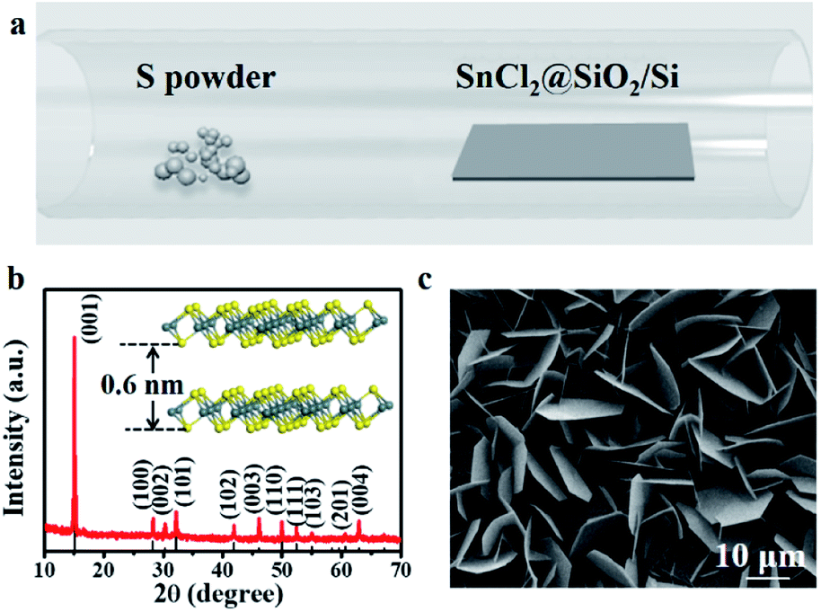 | ||
| Fig. 1 (a) A schematic diagram of the CVD method. (b) XRD patterns of the as-grown nanosheets. Inset: crystal structure of the layered SnS2 crystals. (c) A low-magnification SEM image of as-grown SnS2 nanosheets. | ||
We then verified the as-grown SnS2 nanosheets using Raman spectroscopy. There are always two different polytypes (2H and 4H) in the two-dimension SnS2 crystals.24 In 4H-SnS2 crystals, the most intense Raman peak at 313.5 cm−1 is from a mixture of A1 and E optical modes, and the peaks at 200 and 214 cm−1 are identified to be the E-mode. In 2H-SnS2 crystals, the most intense peak at 315 cm−1 is assigned to the A1g mode, and the peak at 205 cm−1 is ascribed to the Eg mode. And if the thickness decreased down to the nanoscale, the Eg peak couldn't be detectable because of the reduction in the scattering centers for in-plane scattering in the ultrathin SnS2 nanosheets.25 Compare with the Raman spectra of the as-grown SnS2 nanosheets, it's easy to find the SnS2 nanosheets belong to 2H-SnS2 (Fig. 2a). Raman mapping (Fig. 2b) demonstrated the uniformity of the as-grown SnS2 nanosheet. The thickness of the SnS2 nanosheet was about 9 nm from the result of the atomic force microscope (AFM), as shown in Fig. 2c. According to a monolayer thickness of ≈0.6 nm, the nanosheet was about 15 layers. SnS2 is a semiconductor with an indirect bandgap of ∼2.2 eV, the bandgap remains indirect in few-layer and monolayer flakes, which has been demonstrated by theoretical and experimental studies.24 The PL spectra in Fig. 2d showed the bandgap of the as-grown SnS2 nanosheet was ≈2.2 eV, which confirmed it had a high-quality crystalline structure.
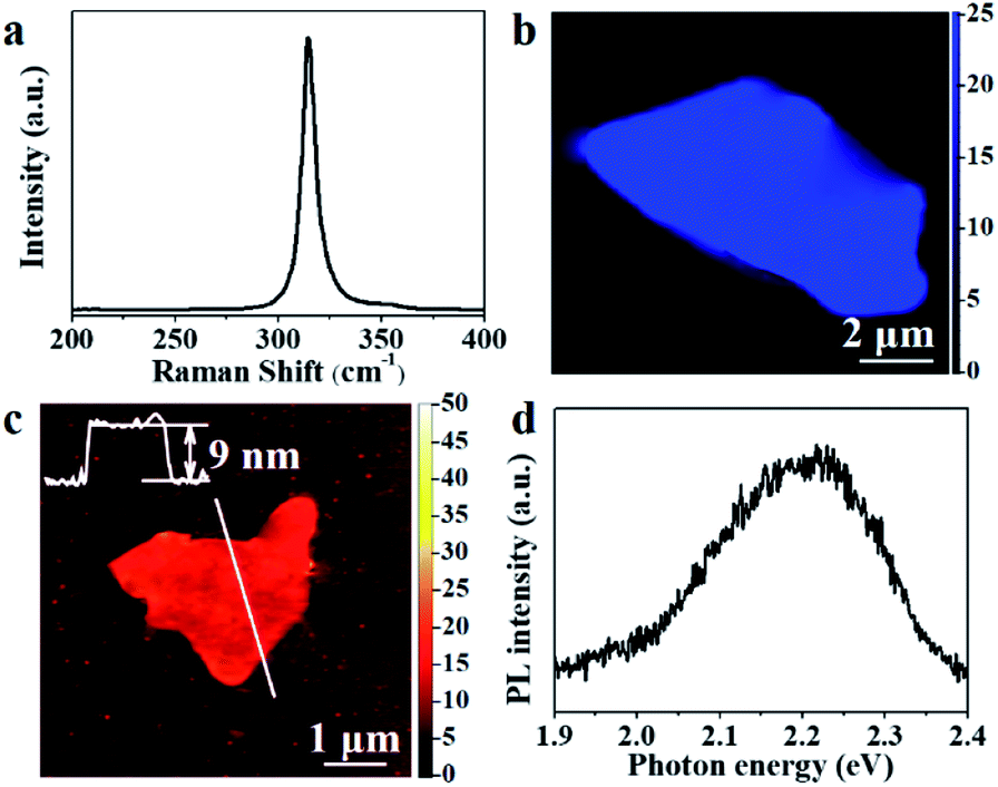 | ||
| Fig. 2 (a) Raman spectrum of SnS2 nanosheet. (b) Raman mapping data of SnS2 nanosheet. (c) Typical AFM image of SnS2 nanosheet. (d) PL spectra of SnS2 nanosheet. | ||
To further evaluate the quality of as-grown SnS2 nanosheets, we undertook a transmission electron microscope (TEM) to explore the lattice structure and the chemical composition information of the sample. Fig. 3a demonstrated a typical low-magnification TEM image of the SnS2 nanosheet. The corresponding high-resolution TEM image in Fig. 3b showed the hexagonal lattice fringes, indicated the SnS2 nanosheet had a perfect atomic structure with a lattice spacing of 0.316 nm, corresponding to the (01−10) and (10−10) planes. The selected area electron diffraction (SAED) and the sharp diffraction spots apparent in Fig. 3c also proved the high-quality crystalline hexagonal structure of the SnS2. Then, the elemental compositions of the SnS2 nanosheet were acquired by the EDX mapping and the EDX spectrum. The EDX mapping in Fig. 3d and e, indicated the uniform distribution of Sn and S elements. EDX spectrum in Fig. 3f demonstrated the atomic ratio between S and Sn was approximately 2![[thin space (1/6-em)]](https://www.rsc.org/images/entities/char_2009.gif) :1, which was consistent with the expected stoichiometry of SnS2. The TEM results further proved that the as-grown SnS2 nanosheets were high-quality crystalline SnS2.
:1, which was consistent with the expected stoichiometry of SnS2. The TEM results further proved that the as-grown SnS2 nanosheets were high-quality crystalline SnS2.
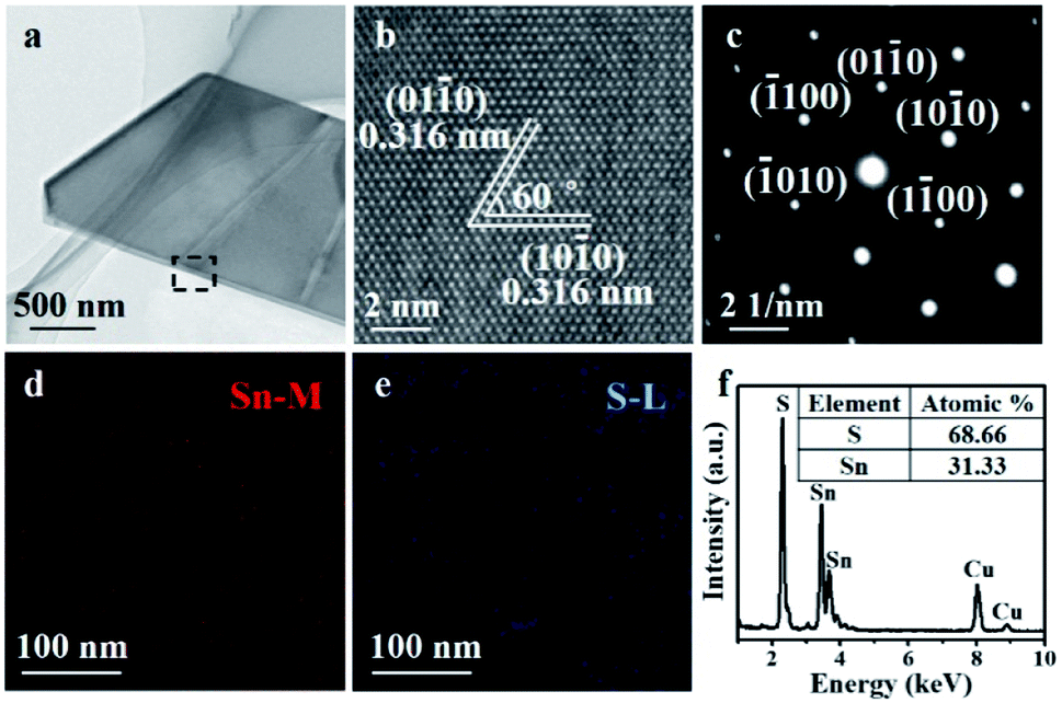 | ||
| Fig. 3 (a) Low-magnification TEM image of the SnS2 nanosheet. (b) High-resolution TEM image and (c) selected area electron diffraction (SAED) pattern image of the SnS2 nanosheet. (d) and (e) Sn and S elemental mapping of the black rectangle region of the SnS2 nanosheet in (a). (f) EDX spectrum of the SnS2 nanosheet, inset: the ratio of Sn and S atoms. | ||
To investigate the optoelectronic properties of the SnS2 nanosheet, photodetectors based on as-grown SnS2 nanosheets have been fabricated. Fig. 4a illustrated the spectral response curve of SnS2 nanosheets from 300 nm to 800 nm. The photoresponse decreased at the wavelength of ≈560 nm (bandgap of ≈2.2 eV), which was consistent with the result of PL in Fig. 2d. I–V characteristics under 680 nm light illumination of 2.1 mW cm−2 and the dark, in air and vacuum of 2.0 × 10⁻² Pa were showed in Fig. 4b. The symmetric behavior of the I–V curves indicated an ohmic contact between the 10 nm Cr/50 nm Au electrodes and the SnS2 channel.26 Regardless of under 680 nm wavelengths or the dark, the currents in vacuum were higher than those in air. It could be explained by an air adsorption/desorption mechanism. Because SnS2 is an n-type semiconductor, its dominant carriers are the electrons. In the dark, the free electrons within the n-type SnS2 channel will be trapped by the air adsorbates on the surface of SnS2 nanosheets. The loss in the area formed on the surface will lead to the decrease of carrier density in the channel.14,27 However, if we turn on the incident light, the combination of the photogenerated holes (separated from electron–hole pairs) and the trapped electrons will release the air adsorbates on the SnS2 surface. It is generally known that the air adsorbates such as oxygen could play an important role in the photoresponse process of other semiconductors especially for 2D semiconductors with a large specific surface area.28 The surface trap states could achieve a longer lifetime of photogenerated carriers and thus guarantee a high Rλ and EQE.29 As the results of the time-resolved photoresponse at a bias voltage of 1 V in air shown in Fig. 4c, the photodetector based on SnS2 sustained a long-time stability response under switching on/off incident light illuminated on it periodically (Fig. 4c). The photo-responsivity (Rλ) of the photodetector was calculated to be 1.4 × 10⁶ mA W−1 through the equation: Rλ = Iph/PS, where Iph = Ilight − Idark is the photoexcited current, P is the light power intensity (2.1 mW cm−2), and S is the effective area under incident light (Fig. 4b inset). Such high responsivity may come from the efficient absorption and optimized device fabrication.14 The external quantum efficiency (EQE) was also evaluated to be 2.6 × 10⁵%, based on the equation: EQE = hcRλ/eλ, where h is the Plank's constant, c is the light velocity, e is the elementary electronic charge, and λ is the excitation light wavelength. The specific detectivity (D*) is 3.1 × 10¹³ Jones according to the equation of D* = RλS1/2/(2e × Idark)1/2. The quality of the photodetector was further determined by fitting the relation of photocurrent and incident light power density with a power law, Iph ≈ Pθ. As shown in Fig. 4d, the exponent θ was fitted to be ≈0.93, suggesting the SnS2 had very few defects or traps to photo-induced electron/hole pairs in the test power density range.30 From response and recovery curves in air (Fig. 4e and f), the rise time of the photodetector was ≈7 ms, while the decay time was ≈6 ms. The performance of our photodetector was more inspiring than the most reported SnS2 based photodetectors shown in Table 1. Such superior responsivity and fast response rates were mainly due to the high-quality crystalline SnS2 structure, large specific surface area, and surface trap states. For example, (a) the high-quality crystalline structure without low density of defects confirmed by the PL spectra and TEM characterizations contributes to a rapid diffusion of charge carriers.31 (b) As well known, large specific surface area due to the ultrathin 2D structure could lead to higher sensitivity and prolong lifetime of photoexcited carriers because of a larger charge separation compared to their bulk counterparts.32,33 (c) Trap states at the surface may prolong the lifetime of photoexcited carriers. Finally, both high responsivity and fast response rates suggest that the surface trapping and recombination relative to the defects reach an equilibrium in the SnS2 photodetector.29
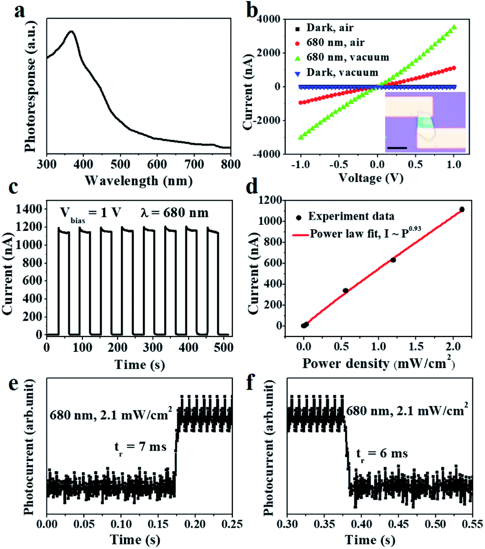 | ||
| Fig. 4 (a) Spectral response curve of the SnS2 nanosheet. (b) I–V characteristics under 680 nm wavelengths and the dark, in air and vacuum of 2.0 × 10⁻² Pa. Inset: the optical image of the photodetector, the scale bar is 10 μm. (c) Time-resolved photoresponse at a bias voltage of 1 V and an illumination power of 2.1 mW cm−2 in air. (d) Photocurrent as a function of illumination intensity at Vbias = 1 V in air. (e) and (f) Response and recovery curves of the photodetector in air. | ||
| Devices | Response range | Wavelength (nm) | Rλ (mA W−1) | EQE (%) | D* (Jones) | Rise time (ms) | Ref. |
|---|---|---|---|---|---|---|---|
| a Rλ – photo-responsivity, EQE – external quantum efficiency, D* – detectivity. | |||||||
| SnS2 | Vis | 532 | 1 × 10⁵ | — | — | 44 | 24 |
| SnS2 | UV-NIR | 830 | 2.1 × 10⁻⁴ | — | — | 460 | 21 |
| SnS2 | Vis | 473 | 1 × 10⁵ | 3.3 × 10⁴ | — | 330 | 34 |
| SnS2 | Vis | 457 | 8.8 | 2.4 | 2 × 10⁹ | 5 × 10³ | 19 |
| SnS2 | Vis | 450 | 2 × 10³ | — | — | 42 | 6 |
| SnS2 | UV-Vis | 405 | 1.5 × 10³ | — | — | 42 | 35 |
| SnS2 | UV-NIR | 532 | 0.65 | 0.15 | 1.13 × 10⁸ | 360 | 27 |
| SnS2 | UV | 350 | 2.6 × 10⁵ | 9.3 × 10⁴ | 1.9 × 10¹⁰ | 20 | 14 |
| SnS2 | Vis | 400 | 1.19 × 10³ | — | 2.4 × 10¹¹ | <1 | 36 |
| SnS2 | Vis | 490 | 1.85 × 10³ | 469 | 4.9 × 10⁹ | 43.4 | 23 |
| SnS2 | UV | 390 | — | 150 | — | — | 37 |
| SnS2 | UV | 365 | 1.1 × 10⁶ | 3.2 × 10⁵ | 9.6 × 10¹¹ | 40 | 38 |
| SnS2 | Vis | 405 | 3.54 × 10⁵ | 1.1 × 10⁵ | 2 × 10¹⁰ | 0.4 | 11 |
| SnS2 | Vis | 532 | 2.08 × 10³ | — | 6 × 10⁶ | 3.4 × 10³ | 39 |
| SnS2 | UV | 350 | 8.6 × 10⁵ | 3.1 × 10⁵ | 1.1 × 10¹⁰ | 700 | 40 |
| BP | UV | 365 | 3.6 × 10⁸ | 1.6 × 10⁶ | 2.3 × 10¹³ | 1 × 10³ | 41 |
| SnS | UV-NIR | 660 | 9.2 × 10⁵ | 1.7 × 10⁵ | 1.09 × 10⁹ | 0.12 | 42 |
| PtS2 | UV-NIR | 830 | 3 × 10² | — | — | 0.1 | 43 |
| PtSe2 | NIR | 632 | 4.5 × 10³ | — | 7 × 10⁸ | 1.1 | 44 |
| PdSe2 | IR | 1064 | 7.1 × 10⁵ | — | 1.3 × 10⁹ | — | 45 |
| SnS2 | Vis | 680 | 1.4 × 10⁶ | 2.6 × 10⁵ | 3.1 × 10¹³ | 7 | This work |
Conclusions
In summary, we have grown a large amount of high-quality SnS2 nanosheets using SnCl2 as the precursors via a CVD method. The as-grown SnS2 nanosheets have been verified by XRD, SEM, Raman/PL, AFM, TEM, and photodetectors, respectively. The SnS2 nanosheet has an indirect bandgap (≈2.2 eV), and its thickness is 9 nm (≈15 layers). The photodetector based on the SnS2 nanosheets exhibits excellent performance, such as a high responsivity (1.4 × 10⁶ mA W−1), a fast response rates (a response time of 7 ms and a recovery time of 6 ms), and a perfect external quantum efficiency (EQE) (2.6 × 10⁵%). This work may provide a new method to grow the SnS2 nanosheets, which could help the research and application of future 2D semiconductor materials.Conflicts of interest
There are no conflicts to declare.Acknowledgements
This study was funded by the Natural Science Foundation of China (grant no. 21701041); the Open Foundation of Hubei Collaborative Innovation Center for High-efficiency Utilization of Solar Energy (grant no. HBSKFQN2017001); and the Talents of High-level Scientific Research Foundation of the Hubei University of Technology (grant no. BSQD2017010).Notes and references
- S. Manzeli, D. Ovchinnikov, D. Pasquier, O. V. Yazyev and A. J. N. R. M. Kis, Nat. Rev. Mater., 2017, 2, 17033 CrossRef CAS.
- Y. Gong, H. Yuan, C. L. Wu, P. Tang, S. Z. Yang, A. Yang, G. Li, B. Liu, V. Jorik and M. L. Brongersma, Nat. Nanotechnol., 2018, 294 CrossRef CAS PubMed.
- X. Zhou, X. Hu, S. Zhou, H. Song, Q. Zhang, L. Pi, L. Li, H. Li, J. Lü and T. Zhai, Adv. Mater., 2018, 30, 1703286 CrossRef PubMed.
- H. Ying, X. Li, Y. Wu, Y. Yao, J. Xi, W. Su, C. Jin, M. Xu, Z. He and Q. Zhang, Nanoscale Adv., 2019, 1, 3973–3979 RSC.
- X. Fu, P. Ilanchezhiyan, G. Mohan Kumar, H. D. Cho, L. Zhang, A. S. Chan, D. J. Lee, G. N. Panin and T. W. Kang, Nanoscale, 2017, 9, 1820–1826 RSC.
- J. Xia, D. Zhu, L. Wang, B. Huang, X. Huang and X.-M. Meng, Adv. Funct. Mater., 2015, 25, 4255–4261 CrossRef CAS.
- T. Yang, B. Zheng, Z. Wang, T. Xu, C. Pan, J. Zou, X. Zhang, Z. Qi, H. Liu, Y. Feng, W. Hu, F. Miao, L. Sun, X. Duan and A. Pan, Nat. Commun., 2017, 8, 1906 CrossRef PubMed.
- B. Giri, M. Masroor, T. Yan, K. Kushnir, A. D. Carl, C. Doiron, H. Zhang, Y. Zhao, A. McClelland, G. A. Tompsett, D. Wang, R. L. Grimm, L. V. Titova and P. M. Rao, Adv. Energy Mater., 2019, 9, 1901236 CrossRef.
- Y. Zhang, P. Zhu, L. Huang, J. Xie, S. Zhang, G. Cao and X. Zhao, Adv. Funct. Mater., 2015, 25, 481–489 CrossRef CAS.
- Z. Zhang, J.-D. Huang, M. Zhang, Q. Yuan and B. Dong, Appl. Catal., B, 2015, 163, 298–305 CrossRef CAS.
- X. Jia, C. Tang, R. Pan, Y. Long, C. Gu and J. Li, ACS Appl. Mater. Interfaces, 2018, 10, 18073–18081 CrossRef CAS PubMed.
- Y. Hu, T. Chen, X. Wang, L. Ma, R. Chen, H. Zhu, X. Yuan, C. Yan, G. Zhu, H. Lv, J. Liang, Z. Jin and J. Liu, Nano Res., 2017, 10, 1434–1447 CrossRef CAS.
- Y. B. Yang, J. K. Dash, Y. Xiang, Y. Wang, J. Shi, P. H. Dinolfo, T. M. Lu and G. C. Wang, J. Phys. Chem. C, 2016, 120, 13199–13214 CrossRef CAS.
- X. Zhou, Q. Zhang, L. Gan, H. Li and T. Zhai, Adv. Funct. Mater., 2016, 26, 4405–4413 CrossRef CAS.
- Y. Sun, H. Cheng, S. Gao, Z. Sun, Q. Liu, Q. Liu, F. Lei, T. Yao, J. He and S. J. A. C. Wei, Angew. Chem., Int. Ed., 2012, 8727–8731, DOI:10.1002/anie.201204675.
- X. Chia, P. Lazar, Z. Sofer, J. Luxa and M. Pumera, J. Phys. Chem. C, 2016, 120, 24098–24111 CrossRef CAS.
- G. Ham, S. Shin, J. Park, J. Lee, H. Choi, S. Lee and H. Jeon, RSC Adv., 2016, 6, 54069–54075 RSC.
- Z. Mutlu, R. J. Wu, D. Wickramaratne, S. Shahrezaei, C. Liu, S. Temiz, A. Patalano, M. Ozkan, R. K. Lake, K. A. Mkhoyan and C. S. Ozkan, Small, 2016, 12, 2998–3004 CrossRef CAS PubMed.
- G. Su, V. G. Hadjiev, P. E. Loya, J. Zhang, S. Lei, S. Maharjan, P. Dong, P. M. Ajayan, J. Lou and H. Peng, Nano Lett., 2015, 15, 506–513 CrossRef CAS PubMed.
- G. Liu, Z. Li, T. Hasan, X. Chen, W. Zheng, W. Feng, D. Jia, Y. Zhou and P. Hu, J. Mater. Chem. AJ. Mater. Chem. A, 2017, 5, 1989–1995 RSC.
- Y. Tao, X. Wu, W. Wei and J. Wang, J. Mater. Chem. C, 2014, 3, 1347–1353 RSC.
- L. A. Burton, D. Colombara, R. D. Abellon, F. C. Grozema, L. M. Peter, T. J. Savenije, G. Dennler and A. Walsh, Chem. Mater., 2013, 25, 4908–4916 CrossRef CAS.
- G. Liu, Z. Li, X. Chen, W. Zheng, W. Feng, M. Dai, D. Jia, Y. Zhou and P. Hu, Nanoscale, 2017, 9, 9167–9174 RSC.
- Y. Huang, E. Sutter, J. T. Sadowski, M. Cotlet, O. L. A. Monti, D. A. Racke, M. R. Neupane, D. Wickramaratne, R. K. Lake, B. A. Parkinson and P. Sutter, ACS Nano, 2014, 8, 10743–10755 CrossRef CAS PubMed.
- J.-H. Ahn, M.-J. Lee, H. Heo, J. H. Sung, K. Kim, H. Hwang and M.-H. Jo, Nano Lett., 2015, 15, 3703–3708 CrossRef CAS PubMed.
- A. Di Bartolomeo, A. Grillo, F. Urban, L. Iemmo, F. Giubileo, G. Luongo, G. Amato, L. Croin, L. Sun, S.-J. Liang and L. K. Ang, Adv. Funct. Mater., 2018, 28, 1800657 CrossRef.
- J.-J. Wu, Y.-R. Tao, Y. Wu and X.-C. Wu, Sens. Actuators, B, 2016, 231, 211–217 CrossRef CAS.
- W. Zhang, J.-K. Huang, C.-H. Chen, Y.-H. Chang, Y.-J. Cheng and L.-J. Li, Adv. Mater., 2013, 25, 3456–3461 CrossRef CAS PubMed.
- X. Zhou, Q. Zhang, L. Gan, X. Li, H. Li, Y. Zhang, D. Golberg and T. Zhai, Adv. Funct. Mater., 2016, 26, 704–712 CrossRef CAS.
- H. Kind, H. Yan, B. Messer, M. Law and P. Yang, Adv. Mater., 2002, 14, 158–160 CrossRef CAS.
- T. Zhai, X. Fang, M. Liao, X. Xu, L. Li, B. Liu, Y. Koide, Y. Ma, J. Yao, Y. Bando and D. Golberg, ACS Nano, 2010, 4, 1596–1602 CrossRef CAS PubMed.
- S. Yang, Y. Li, X. Wang, N. Huo, J. B. Xia, S. S. Li and J. Li, Nanoscale, 2014, 6, 2582–2587 RSC.
- X. Zhou, L. Gan, W. Tian, Q. Zhang, S. Jin, H. Li, Y. Bando, D. Golberg and T. Zhai, Adv. Mater., 2015, 27, 8035–8041 CrossRef CAS PubMed.
- Y. Huang, H.-X. Deng, K. Xu, Z.-X. Wang, Q.-S. Wang, F.-M. Wang, F. Wang, X.-Y. Zhan, S.-S. Li, J.-W. Luo and J. He, Nanoscale, 2015, 7, 14093–14099 RSC.
- C. Fan, Y. Li, F. Lu, H.-X. Deng, Z. Wei and J. Li, RSC Adv., 2016, 6, 422–427 RSC.
- D. Yang, B. Li, C. Hu, H. Deng, D. Dong, X. Yang, K. Qiao, S. Yuan and H. Song, Adv. Opt. Mater., 2016, 4, 419–426 CrossRef CAS.
- G. Ye, Y. Gong, S. Lei, Y. He, B. Li, X. Zhang, Z. Jin, L. Dong, J. Lou, R. Vajtai, W. Zhou and P. M. Ajayan, Nano Res., 2017, 10, 2386–2394 CrossRef CAS.
- Y. Fu, G. Gou, X. Wang, Y. Chen, Q. Wan, J. Sun, S. Xiao, H. Huang, J. Yang and G. Dai, Appl. Phys. A, 2017, 123, 299 CrossRef.
- Y. Wang, L. Huang and Z. Wei, J. Semicond., 2017, 38, 034001 CrossRef.
- J. Yu, A. A. Suleiman, Z. Zheng, X. Zhou and T. Zhai, Adv. Funct. Mater., 2020, 30, 2001650 CrossRef CAS.
- T. Ahmed, S. Kuriakose, S. Abbas, M. J. S. Spencer, M. A. Rahman, M. Tahir, Y. Lu, P. Sonar, V. Bansal, M. Bhaskaran, S. Sriram and S. Walia, Adv. Funct. Mater., 2019, 29, 1901991 CrossRef.
- V. Krishnamurthi, H. Khan, T. Ahmed, A. Zavabeti, S. A. Tawfik, S. K. Jain, M. J. S. Spencer, S. Balendhran, K. B. Crozier, Z. Li, L. Fu, M. Mohiuddin, M. X. Low, B. Shabbir, A. Boes, A. Mitchell, C. F. McConville, Y. Li, K. Kalantar-Zadeh, N. Mahmood and S. Walia, Adv. Mater., 2020, 32, 2004247 CrossRef CAS PubMed.
- Z. Wang, P. Wang, F. Wang, J. Ye, T. He, F. Wu, M. Peng, P. Wu, Y. Chen, F. Zhong, R. Xie, Z. Cui, L. Shen, Q. Zhang, L. Gu, M. Luo, Y. Wang, H. Chen, P. Zhou, A. Pan, X. Zhou, L. Zhang and W. Hu, Adv. Funct. Mater., 2020, 30, 1907945 CrossRef CAS.
- X. Yu, P. Yu, D. Wu, B. Singh, Q. Zeng, H. Lin, W. Zhou, J. Lin, K. Suenaga, Z. Liu and Q. J. Wang, Nat. Commun., 2018, 9, 1545 CrossRef PubMed.
- Q. Liang, Q. Wang, Q. Zhang, J. Wei, S. X. Lim, R. Zhu, J. Hu, W. Wei, C. Lee, C. Sow, W. Zhang and A. T. S. Wee, Adv. Mater., 2019, 31, e1807609 CrossRef PubMed.
| This journal is © The Royal Society of Chemistry 2021 |