
 Open Access Article
 This Open Access Article is licensed under a Creative Commons Attribution-Non Commercial 3.0 Unported Licence
Investigation of oxidation mechanism of SiC single crystal for plasma electrochemical oxidation
Xincheng Yin ,
Shujuan Li*,
Gaoling Ma,
Zhen Jia and
Xu Liu
,
Shujuan Li*,
Gaoling Ma,
Zhen Jia and
Xu Liu
Xi'an University of Technology, Xi'an, Shaanxi 710048, China. E-mail: shujuanli@xaut.edu.cn; Tel: +86-29-82312806
First published on 10th August 2021
Abstract
Silicon carbide (SiC) is a hard-to-machine material due to its high hardness and chemical stability, and usually an essential step in chemical mechanical polishing (CMP) is to modify the SiC surface without introducing damage or other elements, then to polish the modified surface. For high quality and high efficiency surface modification of SiC, a green and promising oxidation approach named plasma electrochemical oxidation (PECO) is proposed. Experiments were conducted to investigate the oxidation mechanism of PECO to enable its application for CMP. The oxidized surface was detected by scanning electron microscope (SEM) and atomic force microscopy (AFM), many atomic-scale protuberances were confirmed to be introduced in the PECO process. Through the analysis of energy dispersive spectroscopy (EDS) and X-ray photoelectron spectroscopy (XPS), it is proved that the SiC surface has been oxidized into SiO2 and a transition layer (silicon oxycarbide) is formed between SiO2 and SiC. Based on the analysis of the cross section image of the oxidized layer, electrolyte–SiC interface chemical reaction and oxidation layer formation mechanism are illustrated to explain the oxidation mechanism. Silicon dioxide growth process model is proposed and illustrated that the phrase of protuberances growth change from charge transfer to diffusion. The present work offers an alternative approach to modify SiC surface, and provides a reference for chemical and mechanical synergetic effect applied in CMP.
1 Introduction
Silicon carbide (SiC) is a promising material as a third generation semiconductor owing to its excellent physical and chemical properties such as wide energy band gap, high thermal conductivity, low coefficient of thermal expansion, high electron mobility and high breakdown electric field, and it has wide application in the fields of electronics, communication, transport, information technology and so on.1–3 To realize a high performance and to meet requirements to fully utilize SiC for wide applications, productive polishing and obtaining a smooth surface without surface scratches or subsurface damage is indispensable. However, conventional mechanical polishing or chemical etching polishing to realize an atomically smooth surface of suitable quality is rather difficult due to its extremely high hardness, high brittleness and remarkable chemical stability. What's worse, surface scratches, pits and pollutant residues can also be introduced. Other polishing attempts like plasma-assisted polishing (PAP),4,5 magnetorheological polishing6 are investigated but only applied in laboratory settings. Chemical mechanical polishing (CMP)7,8 is the most widely used semiconductor wafer polishing technology. It is based on the alternating effect of chemical reaction and mechanical removal to obtain ultra-precision polished SiC surfaces. Many approaches based on CMP have been made to polishing SiC wafers for smooth surfaces, notable among them electrochemical mechanical polishing (ECMP),9,10 electrical enhanced photocatalysis polishing,11 ultraviolet photocatalysis-assisted polishing,12 and UV-photocatalysis assisted chemical mechanical polishing.13 However, all the above polishing brings enormous difficulties obtaining atomically flat smooth surface without subsurface damages. To smooth SiC surface, all the methods, essentially include two steps, oxidize (modify) the SiC surface to produce a softer oxide layer firstly, then mechanically remove the oxide layer by soft abrasive particles. Therefore, the influence of chemical reaction is key to the CMP process.The surface hardness of the modified SiC surface is less than that of the polishing abrasive particles, so that only the oxide layer is removed without damaging the matrix material during the CMP process. To further improve the polishing efficiency and surface quality in the CMP process, it is necessary to form a synergetic effect between the chemical effect of oxidation of SiC surface to form an oxide layer and the removal of the oxide layer by mechanical approach. Thus, a suitable surface oxidation method is vitally important, and different approaches have been proposed for surface modification. Yan et al.12 conducted ultraviolet photocatalysis-assisted polishing for SiC, finding that the material removal rate (MRR) was mainly affected by photocatalytic reaction rate, and the surface roughness was affected by both the reaction rate and abrasive stability. Yuan et al.13 proposed UV-TiO2 photocatalysis assisted chemical mechanical polishing of SiC wafers, under the irradiation of ultraviolet light, holes and electrons are generated on the surface of TiO2 particles since the holes have strong oxidizability, H2O contacting with nano-TiO2 particles is easily oxidized to hydroxyl radicals (˙OH), by which the SiC surface is oxidized into SiO2 oxide layer. However, the photocatalytic activity of TiO2 is greatly affected by UV irradiation. Lu et al.14 proposed that by depositing a thin layer of photocatalytic TiO2 on nanodiamond abrasives to assist polish SiC, in which via ˙OH to oxidize SiC surface and form a relatively soft SiO2 layer. However, the hydrolysis reaction in this process is slow, and surface scratches can be easily introduced by insufficient reaction time. In the process of PAP, the surface of hard to polish materials can be oxidized by plasma radiation, and then the oxidized products can be removed by soft abrasive polishing,15 but the plasma radiation device is complicated. Zhu et al.16 used molecular solid artemisinin (Qinghaosu) crystals to effectively polish SiC wafers in pure water, it was considered that the surface of SiC was activated and oxidized by releasing ˙OH from the internal peroxide bridge by mechanical action. Akihisa Kubota17 utilized a magnetic polishing tool that adsorbs iron particles in the H2O2 solution to polish SiC, in which the ˙OH generated by the iron catalyst particles in hydrogen peroxide solution was used to reduce the micro-roughness of SiC wafer surface. Lu et al.18 carried out SiC CMP experiments based on the Fenton reaction, confirmed that ˙OH chemically react with the SiC surface can form a low-hardness SiO2 oxide layer. The concentration of Fe2+, H2O2 and pH value in Fenton reagent will affect the concentration of ˙OH generated in Fenton reaction, thereby affecting the quality of the polished surface. Deng et al.19 combined the Fe3O4 catalyst and H2O2 oxidant to produce the Fenton reaction, in which ˙OH with strong oxidizability was generated. However, the randomness of the Fenton reaction process makes the concentration of ˙OH uncontrollable. Kentaro Imamura et al.20 developed a method to flatten the Si surface of SiC by electrochemical reaction, but carbon rich layer was easily left on the surface. All those methods have their limitations or drawbacks for SiC surface oxidation in CMP processing, herein, it is necessary to develop a feasible surface modification method for CMP.
Since the effect of SiC surface chemical reaction is crucial to CMP, the research presented in this paper attempts to modify SiC surface without introducing subsurface damage or other elements. To obtain a flat and smooth surface for further processing, a green and promising surface modification method named plasma electrochemical oxidation (PECO) is proposed. This method modifies the SiC surface into a SiO2 oxide layer through oxidation, and the binding force between SiO2 and SiC matrix is reduced, which is easy for the soft abrasive mechanical remove in the CMP process. For a deep understanding of the surface modification characteristic and the balance between oxide formation and mechanical removal in CMP process, it is necessary to investigate SiC oxidation mechanism in PECO. In this study, PECO experiments were conducted and the oxidized surfaces were observed. The oxidation performances such as surface quality, oxide composition and chemical structure were analyzed. Through the analysis of the SiC oxidation layer formation process, a probable SiC oxidation layer formation mechanism in PECO is proposed. This work offers an alternative approach to modify SiC wafers for efficiency promotion in CMP.
2 Principle and experiment of PECO
2.1 Principle of PECO
Fig. 1 shows the SiC-solution interface and oxygen plasma formation process. When the electrodes are conducted, several layers between the SiC-solution interface are formed (Fig. 1(a)). H+ and OH− are produced by the dissociation of H2O molecules. Because OH− discharges preferentially than other negatively charged ions, when the regulated dI/dt is greater, the proportion of precipitated O2 escaping from the solution is smaller, and a dense oxygen film quickly forms on the SiC surface21 (Fig. 1(b)), forming an oxygen bubble layer that much thicker than one atomic layer. Under the effect of the strong electric field on both electrodes, the OH− near the anode lose electrons, the generated Σ4e− electrons move directionally in the electrolyte under the effect of the electric field, and pass through the gas film with high kinetic energy along the gas core wall in the oxygen film in the form of a filamentary current, and randomly collide with O2, in which O2 that obtained electrons is ionized into O2− in a certain proportion in sheath layer (Fig. 1(c)):| H2O → OH− + H+ | (1) |
| 4OH− − 4e− → 2H2O + O2↑ | (2) |
| O2 + 4e− → 2O2− | (3) |
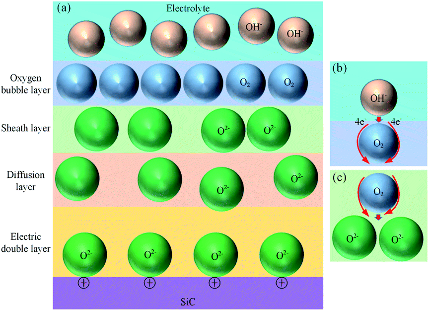 | ||
| Fig. 1 SiC-solution interface and formation process of O2−: (a) SiC-solution interface, (b) oxygen film accumulates on SiC surface, (c) O2− formation. | ||
When sufficient energy is supplied, electrons will move from the cathode to chemical species in solution, and the electron transfer reaction makes the composition of the solution near the SiC surface different from the nearby. Due to concentration gradient, negatively charged ions transport to SiC surface in diffusion layer. The thickness of the diffuse layer region depends on the potential applied to the SiC and on the concentration of ions in the electrolyte. Since the SiC surface is positively charged, it attracts oppositely charged ions (O2−) to the surface, thus the double layer forms, in which the O2− react with SiC.
After the oxygen plasma (O2−) is produced along the convex surface of the oxide film, under the effect of activation energy and electric field, those O2− with high activity react with the Si atoms in the SiC surface layer, thus the Si atoms are oxidized by O2− in atomic thickness:22
| Si + O2− → SiO2 + 2e− | (4) |
On the other hand, the OH− in the electrolyte acts on the surface of SiC, leading to an oxidation reaction:23
| SiC + 6OH− + 6h+ → SiO2 + 3H2O + CO↑ | (5) |
| SiC + 8OH− + 8h+ → SiO2 + 4H2O + CO2↑ | (6) |
The NaCl in the electrolyte enhances the electrical conductivity, and a discharge reaction occurs at the anode, which causes the decomposition of H2O to produce hydroxyl radical (˙OH),24 additionally, the electric field generated by the potential applied to SiC drives the holes (h+) in the SiC bulk to the interface between SiC and the electrolyte, and h+ attracts (OH−) and reacts with it to produce (˙OH):25
| H2O →·OH + H+ + e− | (7) |
| OH− + h+ → ˙OH | (8) |
Since the oxidation potential of ˙OH (2.80 V) is higher than that of oxygen (2.42 V),26 the modification reaction between the surface of SiC wafer and ˙OH27 is:
| SiC + 4h+ + 4˙OH → SiO + 2H2O + CO↑ | (9) |
| SiC + 4˙OH + O2 → SiO2 + 2H2O + CO2↑ | (10) |
In the whole oxidation process, theoretically, O2−, OH−, and ˙OH react with SiC surface and the SiO2 modified layer is generated.
2.2 PECO experiment
Fig. 2 shows a schematic diagram of the experimental setup utilized in this study for SiC PECO processing. The PECO system consists of an AC power supply, electrolytic cell and personal computer (PC). The power supply adopted is a self-made power source developed by Xi'an University of Technology, which controls the oxidation parameters in experiments under the voltage controlled mode. The Al electrode is set as the cathode, the SiC wafer as the anode, which is held by an insulation holder, both the electrodes are immersed in the interior of the glass container. The PECO system's operation is under PC control and experimental data is collected and processed by the PC program. The PECO experimental conditions are listed in Table 1.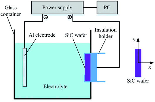 | ||
| Fig. 2 Schematic of PECO setup. | ||
| Parameters | Conditions |
|---|---|
| Voltage | 300 V |
| Current | 2 A |
| Frequency | 20 KHz |
| Duty cycle | 50% |
| Electrolyte | DI water and NaCl |
| Concentration | 0.5 wt% |
| Oxidation time | 5 min |
| Temperature | 25 °C |
Commercial available n-type 4H–SiC (on-axis, off-angle ±0.5°) was provided by Hefei Crystal Technical Material Co. Ltd, its resistivity is 0.015–0.028 Ω m, both faces were prepared by CMP. The Si-face (0001) of the wafer, which is the most commonly used face, subjected to anodize was used in the experiment. The thickness and to-be-oxidized area of the wafer were taken 0.4 mm and 10 mm2, respectively. The electrolyte is deionized water and sodium chloride (NaCl) with a concentration of 0.5 wt%. Before experiments, the SiC wafer was cut into samples with a size of 13 mm × 13 mm×0.4 mm, and then the sample surfaces were polished by conventional approach. The surface contaminants were removed by immersing in H2SO4 (97 wt%) for 30 minutes, and then dipped into concentrated HF solution (40 wt%) for 30 minutes to remove natural oxides on the surface, after that, ultrasonically cleaned with deionized water for 10 minutes and dried in pure N2 gas finally.
To study the SiC surface characteristics after plasma electrochemical oxidation and the oxide layer formation mechanism, the surface and cross-section of the oxide layer were measured and analyzed by various instruments. The surface morphologies of the as-received surface and oxidized surface were measured by scanning electron microscope (SEM, VEGA3 TESCAN). The surface morphology before and after oxidizing was observed by atomic force microscopy (AFM, Bruker AXS Innova). Energy dispersive spectroscopy (EDS, VEGA3 TESCAN) was used to confirm the oxide layer elementary composition. To estimate the oxide layer structure, the cross section was observed by a focused ion beam system (FIB, JEOL JIB-4000), the oxidized surface with local dislodged area was observed by Ultra-Depth Three-Dimensional Microscope (KEYENCE, VHX-2000). All the measurements were conducted at room temperature.
3 Results and discussion
3.1 Surface characteristics after PECO
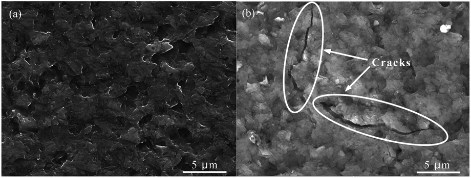 | ||
| Fig. 3 Surface morphology of SiC surface before and after oxidation: (a) as-received surface, (b) PECO processed surface. | ||
Since the morphology is based on the surface roughness measurement to explain the mechanism of plasma electrochemical oxidation. Fig. 4(a) and (b) show the surface morphology of the as-received surface and oxidized surface measured by AFM with the measured area of (5 μm × 5 μm). In Fig. 4(b), it observes that the surface roughness after oxidation treatment is significantly rougher by the random and uneven oxidation. Due to the uneven oxidation of the surface, larger oxide protuberances are generated and distributed on the oxidized surface. With the oxidation reaction going on, the number of oxide protuberances increases, and the surface roughness is greatly affected by the oxidation rate of different parts.28 From the cross-sectional view of Fig. 4(c) and (d), the oxide's maximum height is 286.23 nm, this is because the oxide protuberances are related to the oxidation sites on the surface, and the roughness increases significantly at the locations of the oxide protrusions and corresponding to the subsurface damage.
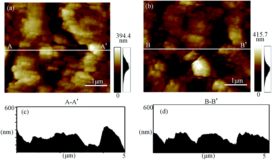 | ||
| Fig. 4 AFM images of (a) as-received surface and (b) oxidized surfaces. Cross-sectional views along (c) A-A′ and (d) B-B′, respectively. | ||
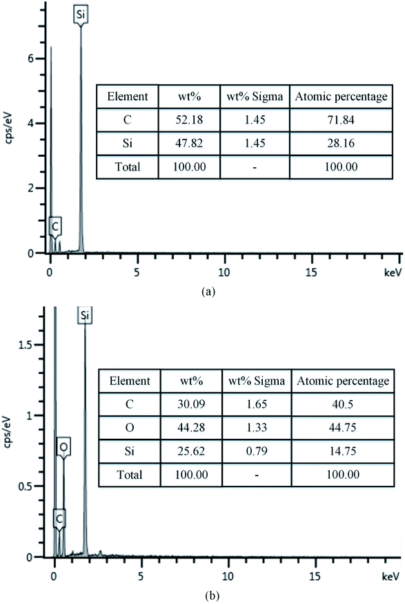 | ||
| Fig. 5 SiC surface composition of (a) as-received surface and (b) oxidized surface. | ||
To confirm that whether there exists intermediate oxide, Fig. 6 shows the Si 2p spectra of the SiC Si-face processed before and after PECO and oxidized surface etched by hydrofluoric acid (HF), which were measured by XPS. In Fig. 6(a), only the characteristic peak of Si–C bond is observed on the as-received surface. After oxidation, the content of Si–C bond decreases, while the O element increases sharply due to a large amount of oxide produced on SiC surface and the appearance of the characteristic peak of the Si–O bond, as shown in Fig. 6(b). The results indicate that the SiC surface was oxidized to SiO2 layer. Meanwhile, the Si–O and Si–C–O bonds with strong peaks can be observed, which indicates that besides the SiO2 layer, there exists certain intermediate oxide with Si–O–C elements. Since SiO2 can be etched by HF, the oxidized samples were dipped in HF solution to remove the oxide. From the Fig. 6(c) it can be found that the characteristic peak of Si–C–O bond still exists except the characteristic peak of Si–C bond, this indicates that there is a Si–O–C element transition oxide layer at the interface between SiO2 and SiC, called transition layer (silicon oxycarbide). That is, during the oxidation process, SiOxCy and SiO2 are formed successively on the surface of SiC.
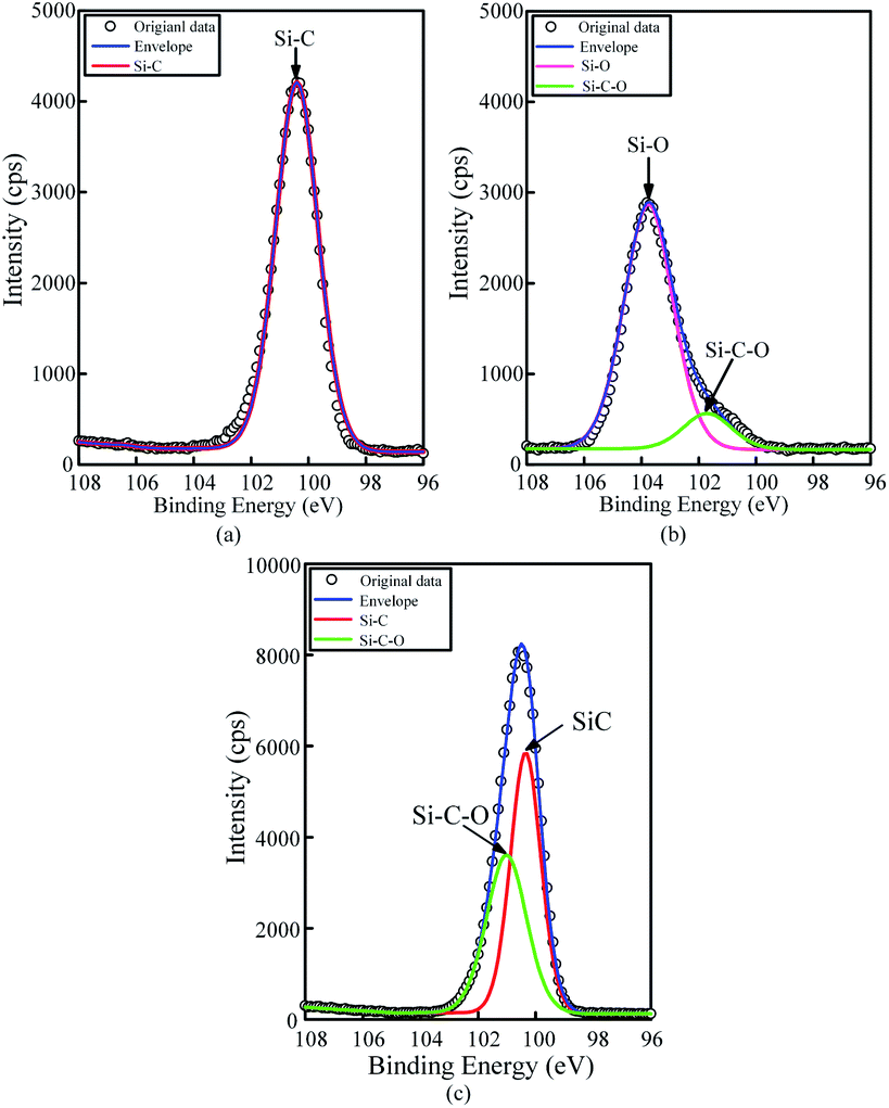 | ||
| Fig. 6 XPS spectra of (a) as-received surface, (b) oxidized surface, and (c) oxidized surface etched by HF. | ||
3.2 Analysis of the oxidation layer formation process
After rough polishing of the SiC surface, a large amount of C–Si bonds and C–C bonds are exposed, thus, the formed dangling bonds can be easily removed or reconstructed through reacting with other external atoms. When the oxidation starts, the oxidant ions quickly approach the surface of SiC. Due to the intervention of the oxidant, the C–Si bonds and C–C bonds are broken, resulting in the fracture of the bonds between Si and C atoms. Thus Si and C atoms are combined with O atoms to form new bonds such as Si–O and C–O and Si–C–O.Fig. 7 shows a cross-sectional micrograph of the oxide layer. The top layer is a carbon layer, which serves as a protective layer during the manufacture of FIB samples. The middle layer covered by the carbon layer is an oxide layer with a thickness of about 4 μm, and the bottom layer is a matrix SiC. The oxide layer structure is well-ordered due to the chemical effect. Since the bond dissociation energy of Si–Si (310 kJ mol−1) is lower than that of Si–C (447 kJ mol−1),29 during the oxidation process, O atoms preferentially interact with Si atoms and accept electrons from Si,30 Si–Si bond is preferentially dissociated. As the reaction continues, a thick SiO2 oxidation modified layer is formed on the top of SiC. Combined with the XPS results, it can be confirmed that there is a silicon oxycarbide transition layer between the SiO2 oxide layer and SiC bulk. Since most of the C atoms in the early oxidation stage stay near the SiC–oxide interface, the resulting oxide contains SiOxCy instead of just only SiO2.
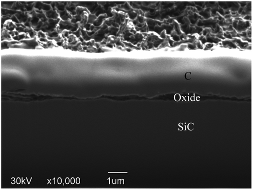 | ||
| Fig. 7 Cross section image of oxidized sample. | ||
The anodic oxidation rate of SiC is very high, due to the loose and porous characteristics of its oxide layer, the depth of the oxide layer can reach micron level after continuous oxidation.31 Fig. 7 shows the cross section of SiC oxide layer, an obvious layered structure can be observed. Because oxidation is produced by surface reaction rather than controlled by O diffusion,32 after a period of continuous oxidation, the diffusion of O into SiC is inhibited by the modified layer and transition layer to a certain extent, which slows down the further oxidation. Meanwhile, the generated gaseous CO2 escapes from the SiC surface, which reduces the bonding force between the SiO2 oxide layer and the SiC matrix. With the continuous formation of the SiO2 layer, the number of surface defects is reduced, and the boundary between oxide layers becomes more and more obvious. Combined with the above analysis, it can be confirmed that gaseous CO2 is generated and SiO2 oxide layer is formed on the SiC surface after PECO treatment.
Fig. 8 shows the sample surface oxidized in different PECO times, which were observed by KEYENCE Microscope. It can be seen that there are obvious changes on the surface with the increase in PECO processing time. Fig. 8(a) shows some small oxidized protuberances have been generated on the SiC surface, indicating that the growth of protuberances occurs in the initial oxidation stage. It can be seen from Fig. 8(b) that with the increase of processing time, the oxidized protuberances grow larger and some oxide layer has formed, indicating that the oxide is quickly formed on the SiC surface. In Fig. 8(c), some part region is not fully oxidized due to the uneven oxidation, while the central part region is over-oxidized that some local dislodged areas have appeared on the oxidized surface, this is because the formation of oxidized particles is also a process of volume expansion, as the oxidation time increases, when the SiO2 oxide layer increases to a certain thickness, the adhesion force between the oxide layer and the SiC substrate decreases. As the oxide film thickens, both the oxides expanding and the oxides' inherent slight tension promote the generation and continued expansion of surface microcracks, resulting in part of the oxide layer breaking due to volume expansion.
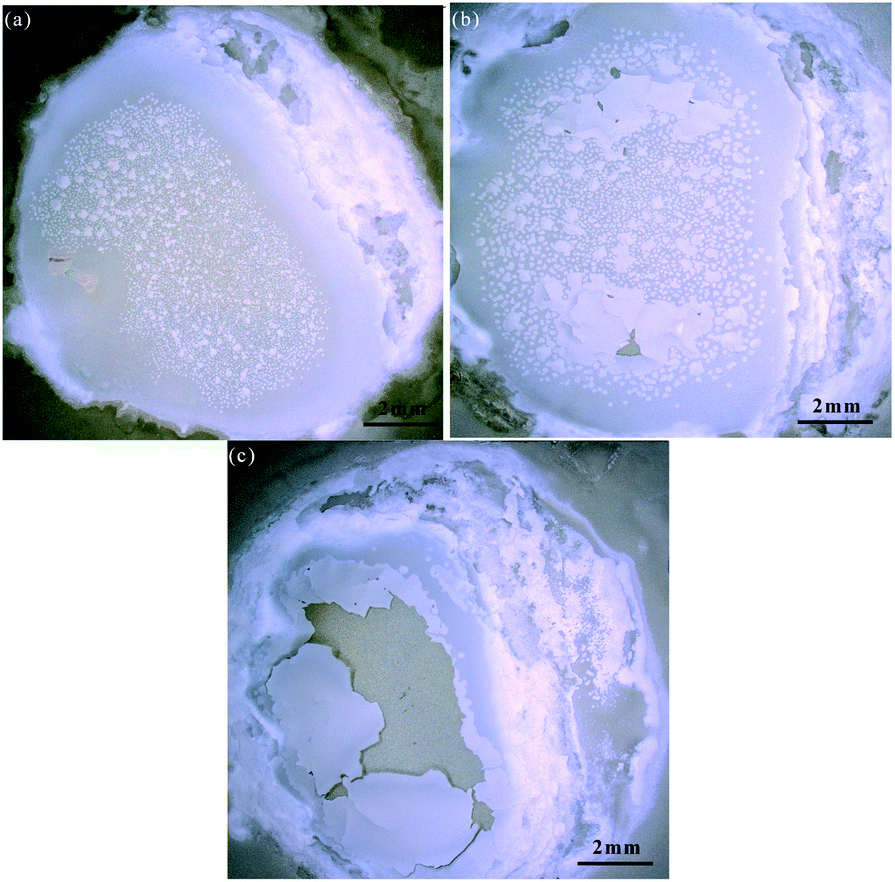 | ||
| Fig. 8 Oxidized surface in different PECO time: (a) 5 s, (b) 10 s and (c) 30 s. | ||
3.3 SiC oxidation mechanism by PECO
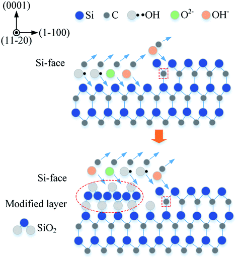 | ||
| Fig. 9 Schematic diagram of interface chemical reaction on Si-face. | ||
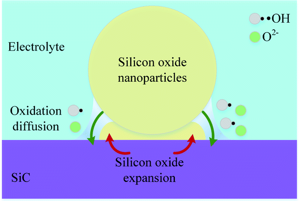
In consideration of the fact that the thin SiO2 film is formed inhomogeneously, Fig. 10 shows the schematic illustration of SiO2 nanoparticle formation process. The oxidant diffuses through the oxide layer to SiC bulk, SiC grains are oxidized into oxide nanoparticles with grain sizes of 20 nm.34 In the growing process of oxide nanoparticles, SiO and SiO2 nanoparticles will be formed at the same time, the generated large tension by silicon oxide expansion leads to the accumulation of amorphous silicon oxide layer, and raise the surface around the silicon dioxide particles, resulting in the formation of oxide bulge. As the oxidation reaction progresses, oxide layers are gradually formed around and below the nano-oxide particles, which are gradually connected together to form a dense oxide surface layer.
 | ||
| Fig. 10 Schematic illustration of SiO2 nanoparticle formation. | ||
The strain caused by the expansion of SiC lattice promotes the oxidation of SiC, and amorphous SiO2 is formed. Since the atomic density of SiO2 is lower than that of SiC, the oxide film ruptures and falls off under the action of the volume expansion force of the oxide layer, the fresh surface of the matrix SiC is exposed to the electrolyte, and the oxidation reaction continues. Thus, the oxide film is continuously generated and accumulating on the fresh surface. As the oxide film thickens, the accumulation of oxide in the transition layer reduces the oxidation rate. The uneven growth of oxide is the main factor that leads to a significant increase in surface roughness.
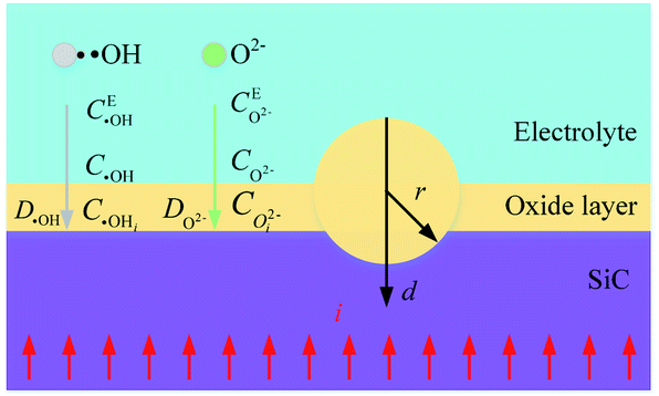
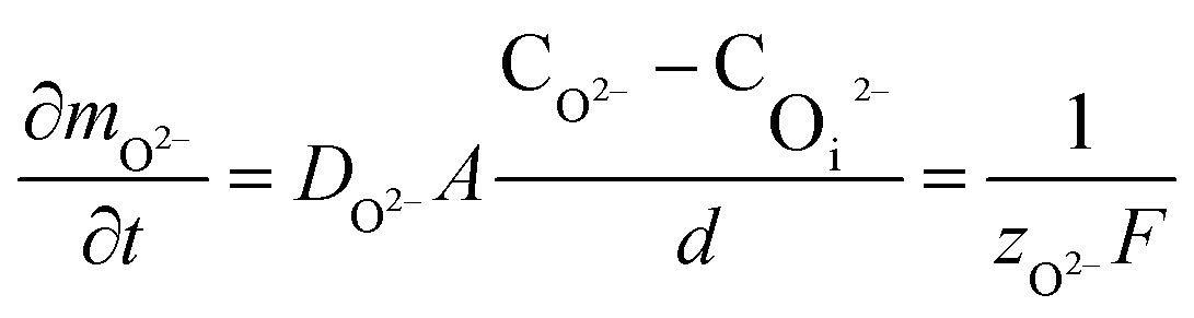
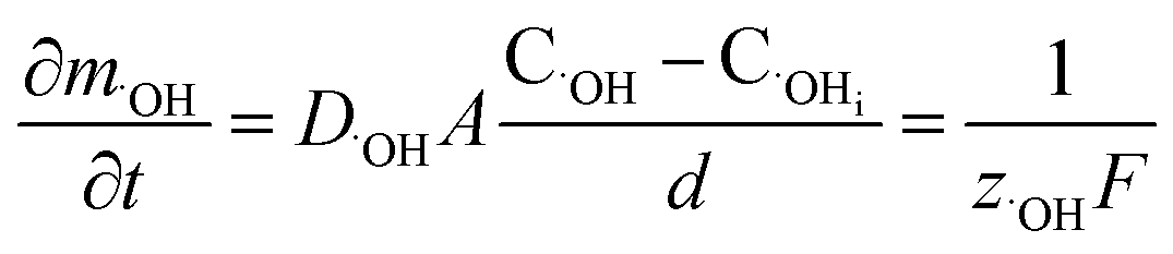
Fig. 11 shows the oxide growth process, the depth of the oxide layer is d, the current density at where oxide protrusions are produced is i. The ions involving in the oxidation reaction are O2− and ˙OH, whose concentrations in the electrolyte are  and CE˙OH, and the concentrations on the surface of the oxide layer are CO2− and C˙OH, and the concentrations in the oxide–SiC interface are COi2− and C˙OHi, and the diffusion coefficients are DO2− and D˙OH in the oxide layer, respectively.
 | ||
| Fig. 11 Schematic of oxide growth process. | ||
Considering that not all charges are involved in the oxidation process, it is assumed that in the oxidation reaction, the number of electrons consumed by O2− and ˙OH are n1 and n2, respectively. The current density i for generating oxide protrusions is:
| i = i1 + i2 = kF(n1COi2− + n2C˙OHi) | (11) |
In the thin oxide state, the interface reaction plays a leading role, that the initial charge transfer process controls the growth of oxide protrusions. When the oxide protrusion grows to a size of 100 nm, it turns into a diffusion process.9 According to Fick's law, in a steady-state condition, the diffusion flux of O2− and ˙OH are:
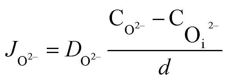 | (12) |
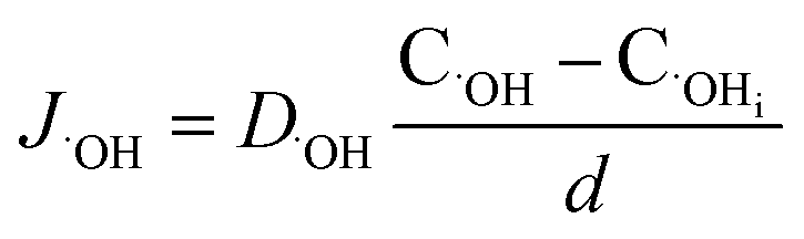 | (13) |
In oxide thickness direction d, the mass transfer rate of O2− and ˙OH are:
 | (14) |
 | (15) |
The concentration of O2− and ˙OH in the oxide–SiC interface are:
 | (16) |
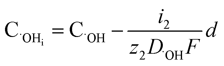 | (17) |
It can be seen from eqn (16) and (17) that both COi2− and C˙OHi decrease with the increase of oxide thickness d. That is, as the thickness of the oxide protrusion increases, the oxidant diffuse through the oxide layer becomes difficult. The diffusion rate of oxidant is limited in the thick oxide layer state, reducing the growth rate of oxide conversely, which is consistent with the results reported in ref. 35.
4 Conclusions
This paper proposed a new SiC surface oxidation method PECO, to promote the oxide formation efficiency in the CMP process. Based on the experimental results, the oxidation mechanism of PECO was clarified from the prospect of electrolyte–SiC interface chemical reaction, SiC oxidation layer formation process and the growth process of silicon dioxide. The following conclusions are obtained.(1) PECO experiment results elucidated that the proposed method is feasible and effective to oxide SiC surface. PECO is a promising approach for semiconductor surface oxidation.
(2) The oxide surface composition and Si 2p spectra of the Si-face of the SiC surface were analyzed, it is confirmed that during the oxidation process, SiOxCy and SiO2 are formed successively on the surface of SiC.
(3) Through the analysis of the SiC oxidation layer formation process, the electrolyte–SiC interface chemical reaction was clarified and a probable SiC oxidation layer formation mechanism in PECO was proposed.
(4) The model of silicon dioxide growth process was proposed based on diffusion theory, it illustrates that the phrase of protuberances growth change from charge transfer to diffusion.
Conflicts of interest
There are no conflicts to declare.Acknowledgements
The research is financially supported by the National Natural Science Foundation of China (Grant No. 51575442), the Natural Science Foundation of Shaanxi Province (Grant No. 2016JZ011, 2019CGXNG-022), and the Shaanxi Province Key Research and Development Plan Project of China (Grant No. 2021GY-275).Notes and references
- A. Oliveros, A. Guiseppi-Elie and S. E. Saddow, Biomed. Microdevices, 2013, 15, 353–368 CrossRef.
- F. Reis, G. Li, L. Dudy, M. Bauernfeind, S. Glass, W. Hanke, R. Thomale, J. Schäfer and R. Claessen, Science, 2017, 357, 287–290 CrossRef CAS.
- F. Roccaforte, P. Fiorenza, G. Greco, R. Lo Nigro, F. Giannazzo, F. Iucolano and M. Saggio, Microelectron. Eng., 2018, 187–188, 66–77 CrossRef CAS.
- K. Yamamura, T. Takiguchi, M. Ueda, H. Deng, A. N. Hattori and N. Zettsu, CIRP J. Manuf. Sci. Technol., 2011, 60, 571–574 CrossRef.
- H. Deng, K. Endo and K. Yamamura, Int. J. Mach. Tools Manuf., 2017, 115, 38–46 CrossRef.
- Y. Bai, F. Zhang, L. Li, L. Zheng and X. Zhang, Acta Opt. Sin., 2015, 35, 0322007 CrossRef.
- V.-T. Nguyen and T.-H. Fang, J. Alloys Compd., 2020, 845, 156100 CrossRef CAS.
- M. Uneda and K. Fujii, Precis. Eng., 2020, 64, 91–97 CrossRef.
- X. Yang, R. Y. Sun, Y. Ohkubo, K. Kawai, K. Arima, K. Endo and K. Yamamura, Electrochim. Acta, 2018, 271, 666–676 CrossRef CAS.
- X. Yang, X. Z. Yang, K. Kawai, K. Arima and K. Yamamura, Int. J. Mach. Tools Manuf., 2019, 144, 103431 CrossRef.
- Y. He, Z. W. Yuan, K. Cheng, Z. Y. Duan and W. Z. Zhao, Proc. Inst. Mech. Eng., Part J, 2020, 234, 401–413 CrossRef CAS.
- Q. S. Yan, X. Wang, Q. Xiong, J. B. Lu and B. T. Liao, J. Cryst. Growth, 2020, 531, 125379 CrossRef CAS.
- Z. Yuan, Y. He, X. Sun and Q. Wen, Mater. Manuf. Processes, 2017, 33, 1214–1222 CrossRef.
- J. Lu, Y. Wang, Q. Luo and X. Xu, Precis. Eng., 2017, 49, 235–242 CrossRef.
- H. Deng and K. Yamamura, Curr. Appl. Phys., 2012, 12, S24–S28 CrossRef CAS.
- D. Zhang, Y. Gan, Y.-r. Zhu and F.-h. Zhang, ScienceOpen Research, 2016 DOI:10.14293/S2199-1006.1.SOR-MATSCI.AMNMZS.v1.
- A. Kubota, Int. J. Autom. Technol., 2019, 13, 230–236 CrossRef.
- J. B. Lu, R. Chen, H. Z. Liang and Q. S. Yan, Precis. Eng., 2018, 52, 221–226 CrossRef.
- J. Deng, J. Pan, Q. Zhang, Q. Yan and J. Lu, Surf. Interfaces, 2020, 21, 100730 CrossRef CAS.
- K. Imamura, T. Akai and H. Kobayashi, Mater. Res. Express, 2019, 6, 055906 CrossRef CAS.
- R. R. Nevyantseva, S. A. Gorbatkov, E. V. Parfenov and A. A. Bybin, Surf. Coat. Technol., 2001, 148, 30–37 CrossRef CAS.
- A. L. Yerokhin, X. Nie, A. Leyland, A. Matthews and S. J. Dowey, Surf. Coat. Technol., 1999, 122, 73–93 CrossRef CAS.
- Y. Ke, R. P. Devaty and W. J. Choyke, Phys. Status Solidi B, 2008, 245, 1396–1403 CrossRef CAS.
- B. Sun, S. Kunitomo and C. Igarashi, J. Phys. D: Appl. Phys., 2006, 39, 3814–3820 CrossRef CAS.
- D. Zigah, J. Rodríguez-López and A. J. Bard, Phys. Chem. Chem. Phys., 2012, 14, 12764–12772 RSC.
- B. Sun, M. Sato and J. Sid Clements, J. Electrost., 1997, 39, 189–202 CrossRef CAS.
- Y. Zhou, G. S. Pan, X. L. Shi, L. Xu, C. L. Zou, H. Gong and G. H. Luo, Appl. Surf. Sci., 2014, 316, 643–648 CrossRef CAS.
- X. Yang, R. Y. Sun, K. Kawai, K. Arima and K. Yamamura, ACS Appl. Mater. Interfaces, 2019, 11, 2535–2542 CrossRef CAS PubMed.
- R. Y. Sun, X. Yang, Y. Ohkubo, K. Endo and K. Yamamura, Sci. Rep., 2018, 8, 2376 CrossRef.
- H. Li, Y.-i. Matsushita, M. Boero and A. Oshiyama, J. Phys. Chem. C, 2017, 121, 3920–3928 CrossRef CAS.
- D. H. van Dorp, E. S. Kooij, W. M. Arnoldbik and J. J. Kelly, Chem. Mater., 2009, 21, 3297–3305 CrossRef CAS.
- C. Liu, J. Q. Xi and I. Szlufarska, J. Phys. Chem. C, 2019, 123, 11546–11554 CrossRef CAS.
- X. C. Yin, S. J. Li and P. Chai, Int. J. Electrochem. Sci., 2020, 15, 4388–4405 CrossRef CAS.
- R. Wang, T. Liu, F. Ning, W. Ou, L. Zhang, Z. Wang, L. Peng, J. Sun, Z. Liu, T. Li, H. Sun and G. Jiang, J. Energy Chem., 2019, 30, 90–100 CrossRef.
- Y. Hijikata, Diamond Relat. Mater., 2019, 92, 253–258 CrossRef CAS.
| This journal is © The Royal Society of Chemistry 2021 |