
 Open Access Article
 This Open Access Article is licensed under a Creative Commons Attribution-Non Commercial 3.0 Unported Licence
A significant enhancement of bulk charge separation in photoelectrocatalysis by ferroelectric polarization induced in CdS/BaTiO3 nanowires†
Zhiqi Jiangab,
Zhaohui Xiaoab,
Zui Taoab,
Xu Zhangab and
Shiwei Lin *ab
*ab
aState Key Laboratory of Marine Resource Utilization in South China Sea, Hainan University, Haikou 570228, Hainan, China. E-mail: linsw@hainu.edu.cn
bSchool of Materials Science and Engineering, Hainan University, Haikou 570228, Hainan, China
First published on 3rd August 2021
Abstract
Efficient charge separation, in particular bulk charge separation (BCS), is one of the most critical factors in determining the performance of photoelectrochemical (PEC) water-splitting. The BCS enhancement of CdS/BaTiO3 (CdS/BTO) nanowires (NWs) in photoelectrocatalysis has rarely been reported. This paper describes a remarkable PEC properties promotion of the CdS/BTO NWs, which is confirmed to be a result of the enhanced BCS efficiency induced by the ferroelectric polarization. The vertical arrays of BTO NWs endow fast transfer of carriers. Meanwhile, CdS is decorated uniformly on the surface of BTO NWs, which ensures a wide range of light absorption. After two negative polarizations, the CdS/BTO NWs have successfully obtained a remarkable photocurrent density, achieving 459.53 μA cm−2 at 1.2 V(vs.RHE), which is 2.86 times that of the unpolarized sample. However, after two positive polarizations, the photocurrent density dramatically decreases to 40.18 μA cm−2 at 1.2 V(vs.RHE), which is merely 0.25 times the original value. More importantly, the photocurrent density reaches up to a prominent value of −71.09 mA cm−2 at −0.8 V(vs.RHE) after two successive negative polarizations, which is a 40.87 mA cm−2 enhancement with respect to the sample without poling. Significantly, at −0.8 V(vs.RHE), the BCS efficiency of the CdS/BTO NWs is as high as 91.87% after two negative polarizations. The effects of ferroelectric polarization on the PEC performance of CdS/BTO NWs have been systematically studied. The results demonstrate that ferroelectric polarization, especially negative polarization, results in an internal electric field to tune band bending of CdS/BTO NWs, thus prominently enhancing the PEC performance.
1 Introduction
With the seriousness of environmental pollution and energy shortage, the role of photoelectrochemical (PEC) water splitting has been increasingly explored in recent years,1,2 which could take advantage of solar power to generate electron–hole pairs. Then the electron–hole pairs separate and migrate to the active sites for redox reactions.3 In this process, it takes hundreds of picoseconds for electron–hole pairs to transfer from the bulk to the surface reaction sites after their formation in only a few femtoseconds. By contrast, the recombination of most electrons and holes in the bulk exclusively covers a few picoseconds,4,5 which shows that electron–hole pairs in the bulk prefer to recombine rather than transfer to surface reaction sites. This sluggish bulk charge separation (BCS) is a considerable reason that restricts photocatalytic efficiency.6 The most common strategies to increase the electron–hole pair separation rates are to construct a heterojunction and use co-catalysts.7–9 Nevertheless, these strategies can merely enhance the charge separation on the surface, but barely affect the separation in the bulk.10 Therefore, the BCS process leads inevitably to the excellent charge separation and PEC efficiency.11As early as the mid-1980s, Inoue et al. deposited NiO, TiO2, Pt, Pd, Cu and phthalocyanine on LiNbO3 substrates, and confirmed that the direction of polarization had significant effects on the adsorption performance, hydrogen production capacity, catalytic performance and electrical conductivity of the composites.12–17 And The effect of polarized surface was accounted for a band-bending model. Ferroelectric semiconductors, such as BaTiO3 (BTO),18,19 were taken seriously due to their ability to generate an internal electric field to enhance charge separation in the bulk.20 When an external electric field is applied to the material in a certain direction, the original chaotic ferroelectric domains in the bulk will be oriented to a certain degree, which causes the two surfaces of the bulk along the direction of the external electric field to be enriched with opposite bound charges. The opposite bound charges produce a depolarization field, which can accelerate the charge separation efficiency in the bulk.21 In 2001, Rohrer et al. observed the spatial separation phenomenon that Ag or PbO2 would be photo-deposited on different crystal planes of BTO,22 which indicated that the internal electric field in the ferroelectric crystal was able to separate the photogenerated carriers at a macroscopic distance, and the half-reactions of electrons and holes could arise on different spatial regions on the catalyst planes.23 Recently, Dunn et al. investigated the effect of the ferroelectric dipole on the photocatalytic activity of BaTiO3/α-Fe2O3 and proposed that the enhanced decolourisation rate of BTO-A/α-Fe2O3 was due to the improved charge carrier separation and extended charge carrier lifetime induced by the internal electrical field.24
BTO can apply the internal electric field to enhance the electron–hole pairs separation. However, the wide band gap makes it only absorb ultraviolet light, which still limits the photocatalytic efficiency.25 Thus, combination of such ferroelectric material with small-bandgap semiconductors like CdS is imperative. The nanowire (NW) structure has been shown to be promising structures for photoelectrocatalysis since it enables the electrolyte to permeate the entire electrode structure and provides facile pathways for electron transport along the length of the wires.26–29 Wang et al. successively coated BaTiO3 and SrTiO3 on the TiO2 nanoarrays photoanodes and it could carry out ferroelectric polarization by applying electrochemical bias and utilized morphological superiority of TiO2 nanoarrays to enhance the separation and transfer of charges.30,31 Wang's team introduced piezoelectricity in TiO2 nanoarrays by coating BaTiO3, and then deposited Ag2O to improve the light absorption efficiency.32
Expect to exploit the unique ferroelectric polarization of ferroelectric semiconductors like BTO to improve charge separation is bound to be a crucial development trend of PEC water splitting in the future.33,34 The researchers eagerly hope for the ferroelectric polarization properties of BTO for high-performance photoelectrocatalysis, but most current systems are about TiO2 nanoarrays,30–32 and there is little systematic study on ferroelectric polarization of pure BTO photoanodes. A recent report by Zhu et al. presented an improved PEC property of the BaTiO3/BaTiO3−x/CdS composite nanocubes due to the extended visible-light absorbance and polarization modulation.18 However, it has not quantitatively verified the effect of ferroelectric polarization on the bulk charge separation. This information is not only instructive for understanding the role of ferroelectric polarization in BTO, but also important for the reasonable design and optimization of BTO-based electrode system to obtain efficient PEC performance.
In this work, BTO NWs were directly used as the substrate, and the ferroelectric polarization was performed by the electrochemical bias method in order to achieve the purpose of efficient charge separation in the bulk. In addition, a layer of CdS sensitizer was deposited onto BTO NWs to serve as a light-absorbing motor and form a visible-light active heterostructure. The effects of ferroelectric polarization on the BTO NWs-based electrodes have been deeply and systematically studied, which provides significant guidance for future research on high-performance PEC electrodes based on ferroelectric materials. Such information is also of significance for development and optimization of electronic systems related to ferroelectric polarization.35–43
2 Experimental
2.1 Fabrication of CdS/BTO NWs
BTO NWs were prepared by two-step hydrothermal method.44 Ti foil substrates (99.9%, 0.01 mm thick) were firstly cleaned in a bath sonicator with acetone, ethanol and deionized water solution, respectively. Sequentially, they were calcined in a furnace at 750 °C for 8 h to form a layer of TiO2 on the surface. Then the Ti foil with TiO2 layer was transferred into the Teflon lined autoclave with 11 M NaOH (fill factor was 65%). After that, the autoclave was placed in a constant temperature oven at 210 °C for 8 h to generate Na2TiO3 (NTO) NWs. The resulting samples were flushed with ethanol and deionized water and dried at room temperature. Finally, Ti foil with a layer of NTO NWs were transferred to Teflon lined autoclave filled with 0.05 M Ba(OH)2 (fill factor was 33%) to keep 210 °C for 12 h in an oven. Then the resulting sample was rinsed with 0.02 M HCl, deionized water and ethanol gently. After drying the BTO NWs samples were finally obtained.CdS layer was decorated on the surface of BTO NWs by the successive ionic layer adsorption and reaction (SILAR) method (referred to as CdS/BTO NWs).45 First of all, the Ti foil with the BTO NWs layer was soaked in 0.2 M Cd(NO3)2 ethanol solution for 30 s, and then rinsed with ethanol several times. The resulting sample was then immersed again in 0.2 M Na2S solution of methanol and water (methanol![[thin space (1/6-em)]](https://www.rsc.org/images/entities/char_2009.gif) :water = 1:1). Then the samples were rinsed with methanol and water solution (methanol:water = 1:1) several times. Above courses were considered as a cycle of CdS deposition. In the experiment, 10, 15 and 20 cycles (C) were conducted respectively to explore the effect of the CdS layers on photocurrent. To avoid the severe photocorrosion and high electron–hole recombination rates of CdS, a ZnS layer was deposited on the outer layer of CdS to restrain the recombination of electrons and holes.46 ZnS was deposited in a similar way to CdS. The samples was soaked in 0.1 M Zn(NO3)2 solution for 1 min, and then rinsed with deionized water several times. Then, the resulting sample was again immersed in 0.1 M Na2S solution of deionized water and methanol (methanol:deionized water = 1:1) and remained 1 min, and then rinsed with deionized water and methanol solution (deionized water:methanol = 1:1) for several times. The preceding processes complete a cycle of ZnS deposition, and a total of two cycles were performed. The as-prepared samples were dried at room temperature. Finally, the samples were annealed on the heating plate at 150 °C followed by 250 °C each for 10 min, respectively.46
:water = 1:1). Then the samples were rinsed with methanol and water solution (methanol:water = 1:1) several times. Above courses were considered as a cycle of CdS deposition. In the experiment, 10, 15 and 20 cycles (C) were conducted respectively to explore the effect of the CdS layers on photocurrent. To avoid the severe photocorrosion and high electron–hole recombination rates of CdS, a ZnS layer was deposited on the outer layer of CdS to restrain the recombination of electrons and holes.46 ZnS was deposited in a similar way to CdS. The samples was soaked in 0.1 M Zn(NO3)2 solution for 1 min, and then rinsed with deionized water several times. Then, the resulting sample was again immersed in 0.1 M Na2S solution of deionized water and methanol (methanol:deionized water = 1:1) and remained 1 min, and then rinsed with deionized water and methanol solution (deionized water:methanol = 1:1) for several times. The preceding processes complete a cycle of ZnS deposition, and a total of two cycles were performed. The as-prepared samples were dried at room temperature. Finally, the samples were annealed on the heating plate at 150 °C followed by 250 °C each for 10 min, respectively.46
2.2 Characterization
The surface morphology of CdS/BTO NWs were examined by scanning electron microscopy (FESEM, Hitachi S4800), and the lattice fringes and energy dispersive X-ray (EDX) element mapping were measured by transmission electron microscopy (JEM-1200EX). Piezoresponse force microscope (Bruker DimensionICON) was used to characterize the ferroelectric and piezoelectric properties of CdS/BTO NWS. X-ray diffraction (XRD) patterns were tested by using Bruker D8 with Cu Kα radiation source. X-ray photoelectron spectrum (XPS, Thermo escalab 250Xi), applying a monochromatic Al Kα source, was used to analyze the chemical composition of the CdS/BTO NWs. The optical properties were measured by UV-Vis spectroscopy (Persee, TU-1901). Photoluminescence spectra were recorded on a JY HORIBA FluoroLog-3 spectrophotometer with the excitation wavelength at 350 nm. Electron paramagnetic resonance (Bruker A300-10/12) was used to detect the free radical species in PEC reactions by CdS/BTO NWs. The incident phonon-current efficiency (IPCE) was tested by employing a 500 W xenon lamp fitted with different monochromatic filters.2.3 Poling process of the electrodes
Ferroelectric polarization was applied using an electrochemical workstation in a three-electrodes configuration. The CdS/BTO NWs electrode was used as the working electrode, while the graphite rod and Hg/HgO electrodes were employed as the counter and reference electrodes, respectively. The electrolyte was a mixed solution of 0.2 M Na2SO3 and 0.1 M Na2S. To endow the nanowires with positive (negative) polarization, the CdS/BTO NWs electrode was polarized with a +3 V (−3 V) voltage for 10 min in the electrolyte.2.4 Photoelectrochemical measurements
The PEC performance of the CdS/BTO NWs were characterized by an electrochemical workstation (Zahner Zennium) equipped with a 500 W xenon lamp (AM 1.5 G, 100 mW cm−2). Three-electrodes system was applied during the experiment: the sample to be tested was used as the working electrode, while the Pt and Hg/HgO electrodes were employed as the counter and reference electrodes, respectively. The electrolyte was a mixed solution of 0.2 M Na2SO3 and 0.1 M Na2S. All the linear sweep voltammetry (LSV) curves were tested with a scan rate of 10 mV s−1. Electrochemical impedance spectroscopy (EIS) tests were performed under the above light source condition, with an amplitude of 10 mV and a frequency from 0.1 Hz to 100 kHz. The degradation experiments were carried out under the radiation of 500 W xenon lamp equipped with a 420 nm filter using an exposed area of 1.5 cm2 in a solution which was composed of 10 mL 0.02 g L−1 methyl orange (MO) and 30 mL preceding electrolyte. The variation of MO concentration was measured by UV-vis spectrophotometer. Polarization experiment was conducted on the CdS/BTO NWs electrode under light illumination, while the polarization voltage was ±3 V and the light source was 500 W xenon lamp (AM 1.5 G, 100 mW cm−2).3 Results and discussion
3.1 The preparation process and morphology
Fig. 1a illustrates the preparation process of the CdS/BTO NWs photoelectrodes. The key preparation steps in this study are the synthesis of precursor NTO NWs and subsequently converting them into BTO NWs. The morphology of BTO NWs generated by hydrothermal reaction highly relies on the morphology of the precursor NTO NWs and the reaction parameters selected to maintain the shape.44 Experiments results suggest that the NTO NWs generated at 210 °C for 8 h are extraordinary uniform (Fig. 1b). The prepared NTO NWs have strong ion exchange performance owing to its open layered structure. Therefore, it could function as a precursor for the synthesis of BTO NWs which could preserve the array appearance.47–49 Accordingly, the NTO NWs were used as the precursor to react with mild Ba(OH)2·8H2O solution. As a result, Na+ was substituted by Ba2+ to form BTO NWs array structure.44 Nevertheless, the prolongation of reaction time caused the occurrence of redissolution and growth reactions, which changed the morphology of the BTO NWs and eventually formed aggregates containing surface (Fig. 1c).49,50 To ensure broad light absorption, we deposited a layer of CdS on BTO NWs (Fig. 1d). The TEM and EDS images were measured and demonstrated in Fig. 1e and f. The high-resolution TEM image displays that the tetragonal BTO (Fig. 1e) has a distinct (111) crystal plane with a lattice spacing of 0.231 nm, and CdS has an obvious (101) crystal plane with a lattice spacing of 0.317 nm. Besides, EDX element mapping results in Fig. 1f suggest Cd and S elements uniformly distribute on BTO NWs. | ||
| Fig. 1 (a) Schematic process for fabricating CdS/BTO NWs. SEM images of (b) NTO, (c) BTO and (d) CdS/BTO NWs samples. (e) TEM image of the CdS/BTO NWs sample. (f) EDX element mapping images of CdS/BTO NWs. | ||
3.2 Crystal structure, chemical status and optical property
XRD analysis was performed to obtain information about the crystal structures of the samples, as shown in Fig. 2a. The TiO2 sample reveals a pure rutile TiO2 crystalline phase (JCPDS no. 76-0318). The XRD pattern from the as-synthesized precursor sample shows the majority peaks matching with NTO (JCPDS no. 84-1881). The peaks arise at 2θ = 22.038, 31.497, 38.887, 44.855, 50.613, 55.953, 65.753, 70.357, 74.334, 78.765 degrees, in accord with tetragonal BTO (001), (101), (111), (002), (102), (112), (202), (212), (103) and (113) planes (JCPDS no. 05-0626).44 After CdS deposition, the XRD pattern of BTO remains unchanged except that there is a (002) (JCPDS no. 75-1545) crystal plane of CdS corresponding to a very weak peak at 26.438 degree, owing to the relatively small amount of deposition. In order to explore the phase of samples, XRD analysis of the region around 2θ = 45° was performed. As shown in Fig. S1,† the peaks of BTO and CdS/BTO NWs samples at about 45° show a significant splitting, confirming the formation of tetragonal BTO.51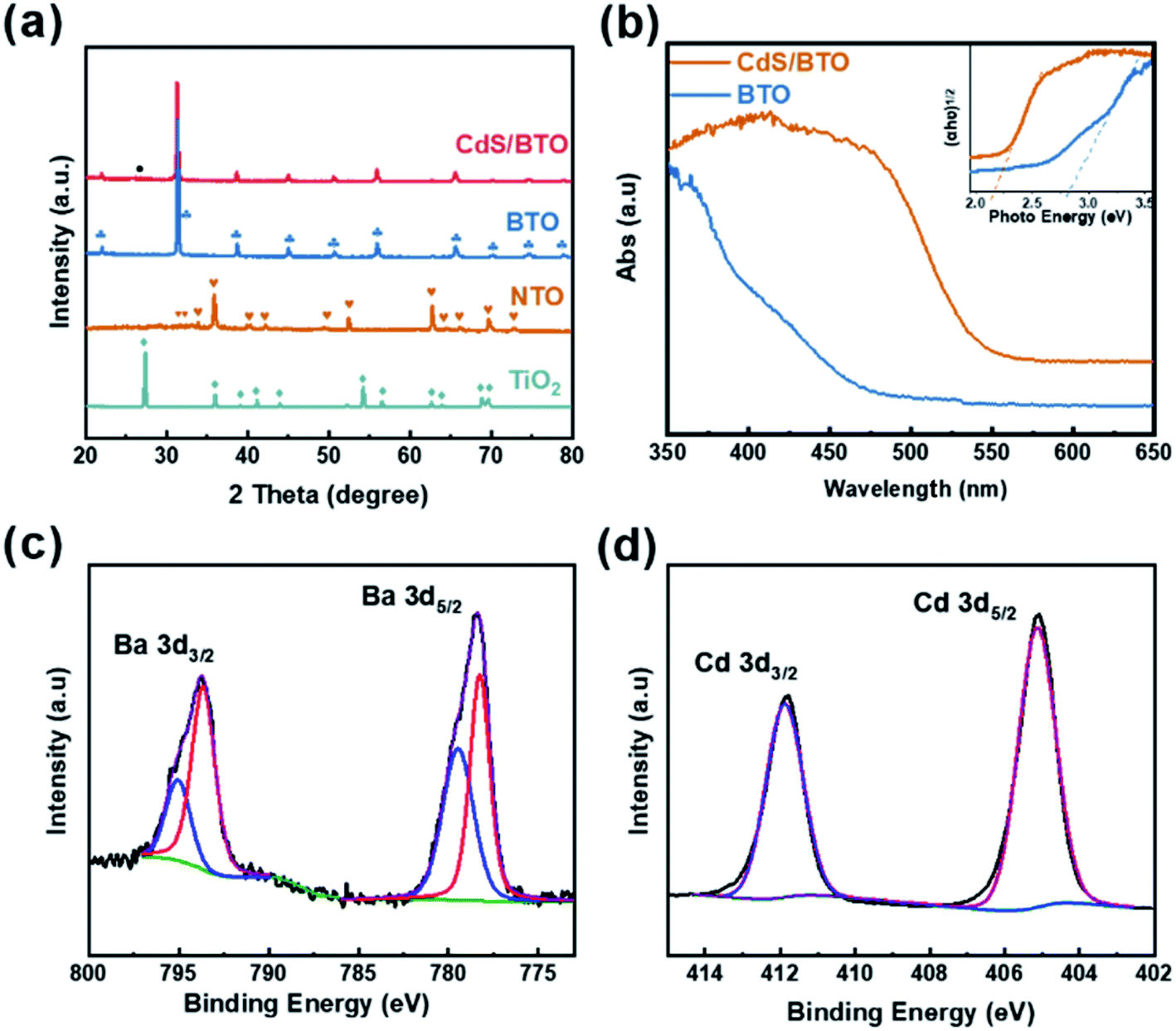 | ||
| Fig. 2 (a) XRD patterns of the TiO2, NTO, BTO and CdS/BTO NWs samples. (b) UV-vis absorption spectra and the inset in (b) presents the corresponding plots of (αhν)2 vs. photon energy. XPS spectra of the CdS/BTO NWs samples: (c) Ba 3d and (d) Cd 3d peaks. | ||
In order to ascertain the variation of surface composition of CdS/BTO NWs, XPS spectra were examined as shown in Fig. S2,† 2c and d. The XPS spectra of the CdS/BTO NWs indicate the existence of the Ba, Ti, O, Cd and S elements (Fig. S2a†). The binding energies of 793.6 and 778.3 eV are Ba 3d3/2 and Ba 3d5/2, respectively, which correspond to Ba atoms in the perovskite structure, while the binding energies of 779.5 and 795.1 eV correspond to Ba atoms in the non-perovskite structure (Fig. 2c).52 And the peaks of Ti 2p1/2 and Ti 2p3/2 at 463.96 and 458.11 eV correspond to Ti4+ band (Fig. S2b†). The O 1 s peaks of BTO at 529.18 and 531.52 eV (Fig. S2c†) represent the Ba–O or Ti–O bonds, and O–H bonds, respectively. The peak at about 533.5 eV is attributed to unavoidable surface physically adsorbed/residual water molecules and/or carbon–oxygen bond in contaminated organic carbon.53 The peaks at 404.9 and 411.7 eV fit to the Cd 3d5/2 and Cd 3d3/2 states, respectively (Fig. 2d), while the peaks at 161.42 and 162.65 eV belong to S 2p3/2 and S 2p1/2 (Fig. S2d†).25
The UV-vis spectra of the BTO NWs without and with CdS overlayer are shown in Fig. 2b. The band gap of CdS/BTO NWs was determined as 2.16 eV from the corresponding Tauc plot (inset in Fig. 2b), which is 0.66 eV less than that of pure BTO NWs (2.82 eV). Compared with pure BTO NWs, the absorption band edge of the CdS/BTO NWs manifests evident red shift.
3.3 Ferroelectric property
Piezoelectric force microscope (PFM) was applied to characterize the domain structures and microdomain properties of the CdS/BTO NWs. It works by capturing the deformation response of the sample under a specific voltage applied by the probe, and then amplifying and outputting the domain structure changes for further analysis. A voltage ramp loop from −6 V to +6 V was applied to the CdS/BTO NWs to test the amplitude change and phase reversals. When an external bias was applied on the ferroelectric sample, the sample produced mechanical vibration due to the inverse piezoelectric effect, and a typical butterfly amplitude curve was obtained (Fig. 3a), demonstrating that the sample has ferroelectric properties. The domain phase reversal induced by an external field is about 180° and thus confirms the ferroelectric feature of the CdS/BTO NWs (Fig. 3b).32 Fig. S3† shows the photocurrent response of the BTO NWs deposited with 10, 15 and 20C layers of CdS. The results show that the photocurrent reaches the optimal value with the 15C CdS layer. Thus, the CdS/BTO NWs samples in the following studies are all the samples deposited with 15C CdS.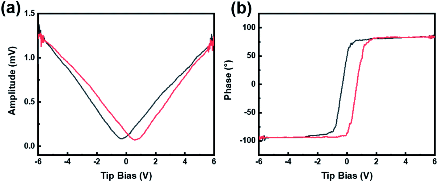 | ||
| Fig. 3 (a) The standard ferroelectric amplitude curves. (b) The phase curves obtained by applying a ramp voltage from −6 to +6 V. | ||
3.4 Photoelectrochemical performance after various polarizations
Fig. 4 shows the LSV curves after two various polarization conditions. In order to investigate the effect of polarization direction on the photocurrent, the CdS/BTO NWs were polarized with twice +3 V (or −3 V) for 10 min, and then followed by one reverse polarization prior to PEC test. We defined the name the sample by using the number of times of polarization and polarization voltage. According to Fig. 4a, after applying −3 V polarizations twice, the photocurrent reaches 390.01 and 459.53 μA cm−2 at 1.2 V(vs.RHE), which are 2.43 and 2.86 times of the unpolarized current (160.46 μA cm−2). However, the photocurrent decreases to 97.56 μA cm−2 at 1.2 V(vs.RHE) after applying the opposite voltage +3 V for the third time. Correspondingly, the photocurrents after twice +3 V polarizations and once −3 V polarization for 10 min achieve 71.08, 40.18 and 487.49 μA cm−2 at 1.2 V(vs.RHE), respectively, which are 0.44, 0.25 but 3.04 times of the unpolarized currents, respectively (Fig. 4b). The results manifest that the negative polarization leads to apparent enhancement of photocurrent while positive polarization causes the opposite results. This effect can be switched with the reversal of the ferroelectric polarization direction. It is worth noting that the dark currents of the samples will also increase or decrease after polarization (Fig. S4†). These results indicate that ferroelectric polarization will also separate some intrinsic electrons and holes in the bulk, and consequently the dark current after polarization will also change accordingly.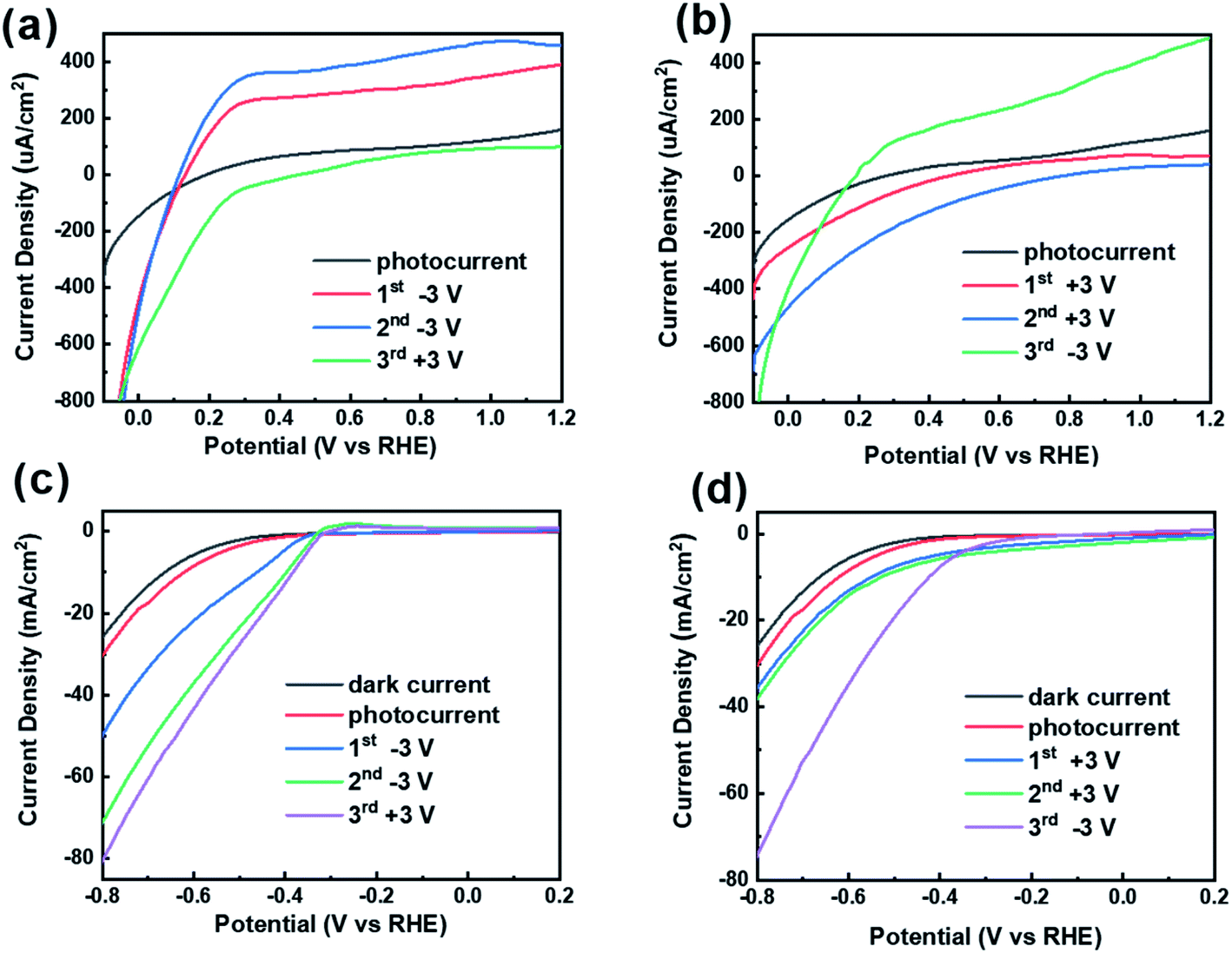 | ||
| Fig. 4 LSV curves of CdS/BTO NWs samples under light irradiation with twice −3 V followed by once +3 V polarizations in (a) positive voltage section (−0.1 V to +1.2 V) and (c) negative voltage section (0.2 V to −0.8 V). And the LSV curves with twice +3 V followed by once −3 V polarizations in (b) positive voltage section and (d) negative voltage section. | ||
Inspired by the consequence that negative polarization promotes the PEC performance, we attempt to explore whether there will be a further PEC improvement in the negative voltage section (−0.8 V to 0.2 V) compared to the positive voltage section (−0.1 V to +1.2 V). Unexpectedly, the results present a remarkable increase in photocurrent in the negative voltage section. To be specific, the photocurrent at −0.8 V(vs.RHE) is −30.22 mA cm−2, which is 188 times that of the photocurrent (160.46 μA cm−2) at the +1.2 V(vs.RHE) (Fig. 4c). The polarization process is the same as before and the polarization duration is also 10 min. At −0.8 V(vs.RHE), the first −3 V, second −3 V and third +3 V polarizations were applied continuously, and the photocurrent were 49.72, 71.09 and 80.44 mA cm−2, respectively (Fig. 4c). On the other hand, after successive application of +3 V, +3 V and −3 V polarizations, the photocurrents reach 35.31, 37.88, 73.98 mA cm−2 at −0.8V(vs.RHE), respectively (Fig. 4d). After once polarization with −3 V or +3 V, the photocurrent increases by 19.36 or 5.08 mA cm−2, respectively. Different from the results in the positive voltage section, in the negative voltage section, either positive or negative polarization can enhance the photocurrent, but the effect of negative polarization is more significant.
In order to reveal the more detailed relationship between the polarization and current response, further LSV experiments were carried out by varying the polarization intensity. We applied a poling voltage varying from −1 V to +1 V and changed the polarization duration from 1 to 10 min (Fig. S5†) to find out why the current in the negative voltage section enhanced so dramatically. All the current was measured in the dark to eliminate the influence of light. On the one side, to explore the influence of polarization intensity on the CdS/BTO NWs, the polarization time was maintained at 1 min and the polarization voltages varied from −0.2 V (0.2 V), −0.4 V (0.4 V), −0.6 V (0.6 V), −0.8 V (0.8 V) to −1 V (1 V), respectively. The results show that the current of the CdS/BTO NWs polarized as photoanode in different intensities reaches the highest 185 μA cm−2 (lowest 48 μA cm−2) at the bias of 1.2 V(vs.RHE), which is 1.31 times more than (0.29 times less than) the sample without poling (Fig. S5a and c†). On the other side, to explore the influence of polarization duration on the CdS/BTO NWs, we set the polarization intensity as −0.5 V or +0.5 V, and changed the polarization duration from 2, 4, 6, 8 to 10 min. The results display that, with the poling voltage of −0.5 V (+0.5 V), as the polarization time increases, the current increases to the maximum value of 124 μA cm−2 (decreases to the minimum value of 35 μA cm−2) for 10 min, which increases by 0.72 times (decreases by 0.59 times) compared with the unpolarized sample (Fig. S5b and d†). The above results show that the current increases by 8.63 μA cm−2 (decreases by 0.21 μA cm−2) even if the poling voltage of −0.2 V (+0.2 V) was applied for 1 min. Such indicates that the CdS/BTO NWs are very sensitive to polarization voltage, and the negative polarization with the same voltage may produce stronger internal electric field than the positive polarization to achieve more charge separation effect. Thus, we consider measuring photocurrent in the negative voltage section as a process of negative polarization, so that the photocurrent in the negative voltage section will be much higher than those in the positive voltage section.
In order to explore the reason why the photocurrent at −0.8 V(vs.RHE) still increases after +3 V polarization as shown in Fig. 4c and d, we applied polarization in the dark for comparison (Fig. S6†). The results show that the dark currents at −0.8 V(vs.RHE) decreases after +3 V polarization without light but increase under the illumination. This suggests that the application of positive polarization alone suppresses the dark current. But the dark current will increase by applying ferroelectric polarization in the presence of light. This is because the CdS overlayer responds well to visible light and measurement process in the negative voltage section itself is a process of applying negative polarization. Although the photocurrents increase greatly after polarization, the dark currents also increase heavily (Fig. S4†). The LSV curves of pure BTO NWs polarized twice at ±3 V for 10 min in Fig. S7† also confirm the speculation above.
To further explore the response ability of CdS/BTO NWs to visible light, the transient photocurrent curves are present in Fig. S8.† When 0 V(vs.RHE) or 0.5 V(vs.RHE) bias was applied to the CdS/BTO NWs, the photocurrents response reached an average of about 12 or 35 μA cm−2, respectively (Fig. S8a and b†). However, when −0.5 V bias was applied, instead of pulse signal, the photocurrent continued to rise from −1.42 to −4.15 mA cm−2 during the 5.5 hours illumination, and then the photocurrent dropped to −3.08 mA cm−2 and remained stable when the light radiation was removed (Fig. S8c†). The transient curves obtained with 0 V and +0.5 V are quite different from that with −0.5 V. The possible reason for these results is listed as follows. Applying a constant voltage of −0.5 V corresponds to applying a ferroelectric polarization at −0.5 V with an ever-increasing polarization time. On the one hand, the BTO NWs deposited with CdS have an active visible-light response and therefore can obtain enhanced photocurrent under light conditions (Fig. S3†). As can be seen from Fig. S5b,† for negative polarization, prolonging the polarization time would increase the current density in response. In addition, the application of negative ferroelectric polarization under light conditions also significantly increases the current compared to that in dark (Fig. S6†). These aspects above work together to increase the photocurrent of the CdS/BTO NWs under the continuous polarization with −0.5 V. When the light radiation was removed, the photocurrent density decreased, but not to the current density before the light was applied. This may be due to the residual ferroelectric polarization, corresponding to the increase of dark current.
In order to explore the stability of samples, LSV, XRD and SEM tests were performed on polarized samples (Fig. S9–S11†). The samples which had been polarized for two months after −3 V/−3 V/+3 V polarization and +3 V/+3 V/−3 V polarization were tested again by LSV in the negative voltage part (−0.8 V to 0.2 V). The results in Fig. S9† show that the samples after −3 V/−3 V/+3 V polarization and +3 V/+3 V/−3 V polarization can still reach 80.29 mA cm−2 and 73.12 mA cm−2 under the same measurement conditions as Fig. 4 after two months, which only reduced by 0.15 mA cm−2 and 0.86 mA cm−2 compared with the previous samples (80.44 mA cm−2, 73.98 mA cm−2). The results show that the polarized CdS/BTO NWs samples are stable after a long time of placement. In addition, we performed XRD tests on the samples after polarization and placed for two months. The XRD results as shown in Fig. S10† indicated that there was almost no change in the phase structure, which once again demonstrated the stability of the samples. In order to observe the changes before and after polarization more intuitively, we presented the SEM image after polarization, which shows no obvious corrosion on the surface after polarization (Fig. S11†).
3.5 Interfacial charge transfer performance
EIS experiments were performed to investigate the charge transfer characteristics of the CdS/BTO NWs under different polarizations (Fig. 5). The equivalent circuit used for modeling the measured electrochemical response is shown in Fig. S12,† while the fitting data are summarized in Table S1.† The working electrode was irradiated by a 500 W xenon lamp (AM 1.5 G, 100 mW cm−2), and the electrolyte was a mixed solution of 0.2 M Na2SO3 and 0.1 M Na2S, and the measurement was conducted with an amplitude of 10 mV. The duration of applying ±0.5 V and ±1 V polarizations was 3 min, and the time of applying ±3 V polarizations was 10 min. The interface charge transfer resistance can be represented by the semicircle diameter of the arc in the Nyquist diagram. Fig. 5a presents that as the intensity of negative polarization increases, the diameter of the arc decreases, indicating that the negative polarization promotes the charge transfer at the interface between the electrode and electrolyte. On the contrary, positive polarization gradually increases the diameter, which is against to charge transfer at the interface. Among them, the diameters of the −3 V polarized samples are much smaller than that of the unpolarized sample, suggesting that the negative polarization to a great extent improves the charge separation efficiency of the CdS/BTO NWs samples. Fig. 5b shows that with the increase of negative polarization, the impedance gradually decreases, but with the increase of positive polarization, the impedance increases significantly. This proves again that negative polarization promotes the PEC reaction, while positive polarization is the opposite. | ||
| Fig. 5 (a) EIS Nyquist plots of the CdS/BTO NWs samples after different polarizations and the inset shows the results for −3 V (1st) and −3 V (2nd). Open circles were test data points and solid lines were corresponding fitting. (b) Impedance change value compared to unpolarized sample of the CdS/BTO NWs samples. | ||
3.6 Bulk charge separation property
The bulk charge separation efficiency (ηbulk) of CdS/BTO NWs was measured according to the recently reported methods (Fig. 6a).15,54 In short, the photocurrent density we measured conforms to the following formula:5| J = Jabs × ηbulk × ηsurface | (1) |
| ηbulk = Jsulfite/Jabs | (2) |
Fig. 2b shows that CdS/BTO NWs begin to absorb light at 580 nm. Thus, by integrating the electron flux of AM 1.5 global filter solar spectrum between 300 and 580 nm,31 the Jabs can be calculated to be 12.05 mA cm−2.5,15,30–32 PEC sulfite oxidation is a powerful means to evaluate the charge separation efficiency, because it could facilitate the thermodynamics and kinetics of the reaction. We assume that the electrons and holes can be completely separated without affecting the charge separation efficiency in the bulk when they reach the surface to react with 1 M Na2SO3. The Jsulfite of CdS/BTO NWs with different polarizations could be obtained by the LSV curves, and the experiments were conducted in 1 M Na2SO3 electrolyte which acted as the hole sacrificial agent under the irradiation of 500 W xenon lamp (AM 1.5 G, 100 mW cm−2).5 According to Jsulfite in Fig. S13,† we can calculate the ηbulk of the no poling, 1st −3 V and 2nd −3 V samples to be 54.36%, 65.56% and 91.87% at −0.8 V(vs.RHE), and 0.36%, 1.35% and 4.96% at +0.8 V(vs.RHE), respectively (Fig. 6a). It is worth noting that after two negative polarizations, in comparison to the no poling sample, the ηbulk rises to 4.96% (13.8 times enhancement) at +0.8 V(vs.RHE) and even rises to 91.87% (1.7 times enhancement) at −0.8 V(vs.RHE). The result confirms the promoting effect of the negative polarization. Li et al. recently reported 80% improvement of the ηbulk in Bi3O4Cl by carbon doping.5 However, in our work, the ηbulk can be increased to about 92% by an even simpler method (applying electrochemical bias), which indicates that ferroelectric polarization can be an effective approach to optimize the PEC performance.
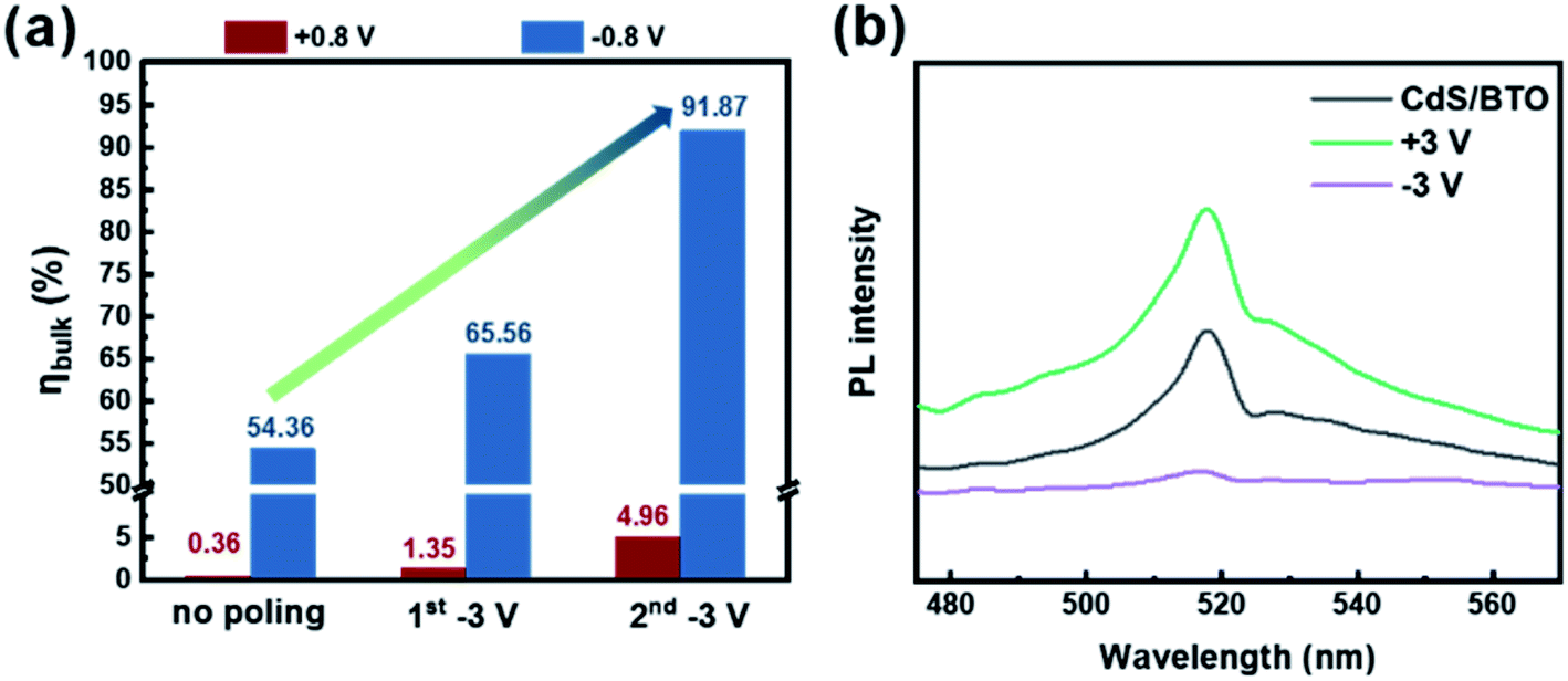 | ||
| Fig. 6 (a) ηbulk of the CdS/BTO NWs samples after different polarizations, (b) PL spectra of CdS/BTO NWs after different polarizations. | ||
The steady-state photoluminescence (PL) spectra (excitation wavelength was 350 nm) were also used to explore the effect of ferroelectric polarization on the charge separation efficiency (Fig. 6b). As the negative polarization intensity increases, the PL strength decreases, while the trend of positive polarization is opposite. This indicates that negative polarization can effectively reduce the recombination rate of photogenerated electrons and holes, while positive polarization promoting the recombination. It is worth noting that the PL intensity not only varies near the excitation peak, but also rises (positive polarization) or drops (negative polarization) throughout the entire waveband. The results imply that the internal electric field generated by ferroelectric polarization might also promote the electron–hole pairs separation of some intrinsic shallow levels inside the semiconductor. This result also explains the increase of dark current after polarization.
The above studies confirm that negative polarization would promote the charge separation efficiency and thus improve the photocurrent density. In order to determine the influence of negative polarization on the PEC performance at a fixed wavelength, the incident photon-to-current efficiency (IPCE) was evaluated at the constant bias of 0 V(vs.RHE) on the CdS/BTO NWs with no poling and negative polarization with −3 V for 10 min. As shown in Fig. S14,† the IPCE rises to the maximum of about 77.5% at 420 nm, which is a 40.6% enhancement in comparison to the unpolarized sample (36.9% at 420 nm).
3.7 Photocatalytic activity
In order to characterize the effect of polarization voltage on the photocatalytic efficiency of CdS/BTO NWs, we examined the MO degradation under the irradiation of 500 W xenon lamp equipped with 420 nm filter (Fig. 7).19,55,56 We carried out the experiment with a constant voltage of ±0.5 V and ±1 V for the degradation of MO, which was equivalent to applying an uninterrupted polarization of ±0.5 V or ±1 V. The blank curve without poling barely degrades MO under light radiation, which indicates that no adsorption occurs during the MO degradation. As presented in Fig. 7a, it's obvious that the value of C/C0 with negative polarization is much greater than that with positive polarization (where C and C0 are MO concentrations under illumination for time t and 0, respectively). The degradation rates after 150 min light exposure are 22.7%, 27.4%, 48.1% and 100% for the CdS/BTO NWs samples with applied biases at 0.5, 1, −0.5 and −1 V, respectively (Fig. 7b).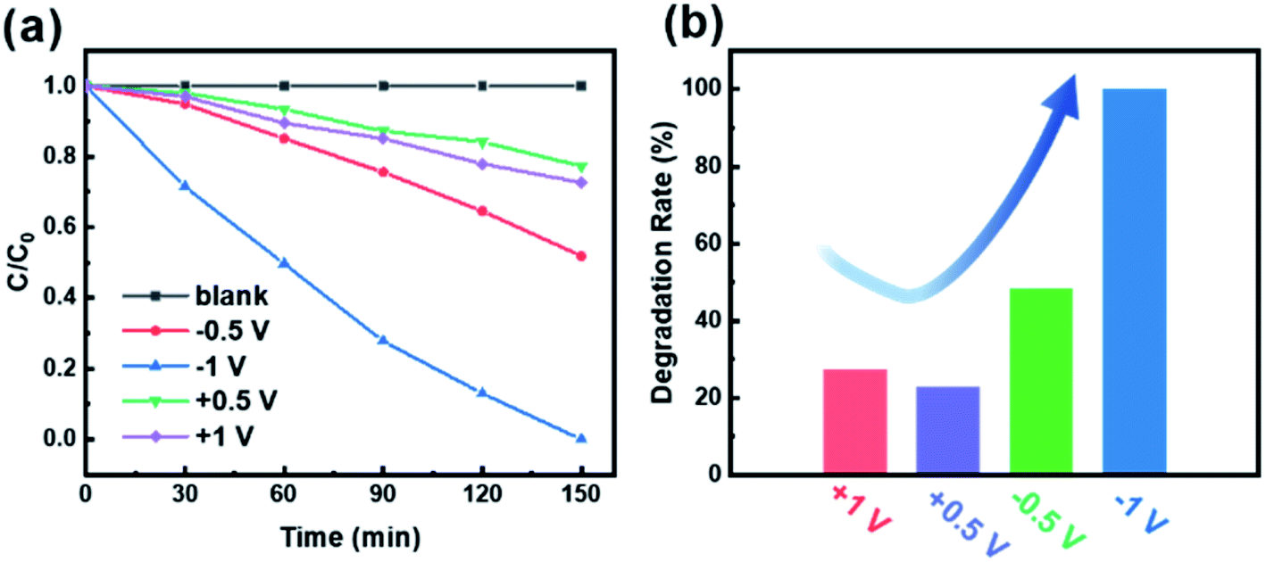 | ||
| Fig. 7 (a) The photoelectrochemical catalytic degradation curves of MO with different applied biases and (b) corresponding degradation rates of the CdS/BTO NWs samples after 150 min. | ||
Trapping technique is an efficient method to identify transient active substances participated in photochemical reactions. Under the irradiation of a 300 W xenon lamp equipped with a 420 nm filter, electron paramagnetic resonance (ESR) was implemented to verify the presence of superoxide (˙−O2) and hydroxyl radical (˙OH) by using general spin probes such as DMPO.32,57 As illustrate in Fig. S15a and b,† pure BTO can produce ˙−O2 and ˙OH, whereas pure CdS can only produce ˙−O2 and cannot produce ˙OH. Fig. S15c and d† present that both ˙−O2 and ˙OH emerge for the CdS/BTO NWs samples with no poling, after −3 V polarization for 10 min and +3 V polarization for 10 min, revealing that both ˙−O2 and ˙OH are the active radical species to degrade MO.58 In comparison to the absence of ˙OH for pure CdS, ˙OH production by the CdS/BTO NWs indicates the key role of BTO NWs under light irradiation.
3.8 Band structure
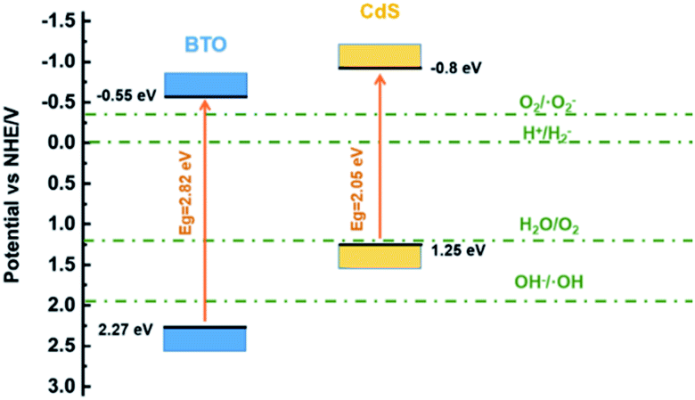
The position of valence band could be ascertained by the valence band XPS spectroscopy. According to the intercept of the tangent line in Fig. 8c and d, the valence band positions of BTO and CdS can be determined as 2.27 eV and 1.25 eV respectively.24 These data also correspond to the ESR results above. The band gaps of 2.82 and 2.05 eV were determined by combining UV-vis spectra in Fig. 8a and b. Thus, the positions of the valence band and conduction band of BTO and CdS can be ultimately confirmed (Fig. 9). Thus, the resulted staggered band alignment can effectively promote the separation and transfer of photogenerated electrons and holes in the CdS/BTO NWs.46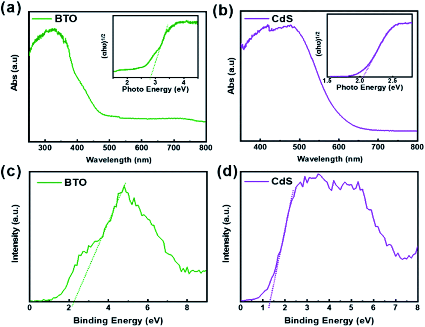 | ||
| Fig. 8 UV-vis absorption spectra of (a) BTO and (b) CdS. The insets in (a and b) present the corresponding plots of (αhν)2 vs. photon energy. Valence-band XPS spectra of (c) the BTO and (d) CdS samples. | ||
 | ||
| Fig. 9 Schematic band structure of the CdS/BTO NWs samples. | ||
3.9 Mechanism
In light of these data, we propose the underlying PEC mechanism as illustrated in Fig. 10. Under the influence of external bias, charges are created at both sides of BTO nanolayer by the ferroelectric polarization, which establish an internal electric field. The orientation of the internal electric field, which is opposite to the polarization, could be switched by the external bias/electric field.59 When the BTO is polarized, the negative polarization will induce an internal electric field with the direction pointing to the electrolyte and an upward band bending at the BTO/CdS interface. The upward band bending is favorable for the electrons to migrating towards the Ti substrate and facilitates the holes transfer to the electrolyte, which ultimately promote the PEC reactions. In the meanwhile, the ferroelectric polarization charges at the BTO/CdS interface contribute to the separation and transfer of photogenerated electron–hole pairs in CdS, thus further enhancing the bulk charge separation efficiency of CdS/BTO NWs. However, when positive polarization is applied, the internal electric field will be switched and point against the electrolyte, which inhibits upward band bending at the BTO/CdS interface. In this case, the bulk charges cannot separate effectively and the PEC efficiency decreases.30–32,59–62 | ||
| Fig. 10 Schematic band diagrams and mechanism for the enhanced PEC performance of the CdS/BTO NWs samples with (a) negative polarization and (b) positive polarization. | ||
4 Conclusions
In summary, we developed an effective method to enhance the bulk charge separation efficiency of the CdS/BTO NWs with ferroelectric polarization and finally enhance PEC performance. The BTO nanowires were prepared by a two-step hydrothermal process, and the subsequent CdS decoration on the outer layer insures wider light absorption of the CdS/BTO NWs. An internal electric field induced by negative ferroelectric polarization by applying an electrochemical bias could result in an upward band bending, which ultimately promotes charge separation and transfer, leading to a prominent enhancement of PEC properties. This work confirms that the ferroelectric polarization could be an effective approach to optimize the PEC behaviors of the electrodes based on ferroelectric semiconductors. In addition, we expect this work can provide some useful hints to realize the efficient and environmentally friendly nanosystems using ferroelectric effect.Author contributions
Z. Jiang conducted the project. Z. Jiang and X. Zhang performed the measurements. Z. Xiao and Z. Tao helped analyze the data. Z. Jiang, Z. Xiao and S. Lin wrote and revised the paper. S. Lin designed and supervised the project.Conflicts of interest
There are no conflicts to declare.Acknowledgements
This work was supported by the National Natural Science Foundation of China (Grant No. 61764003), Major Science and Technology Planning Project of Hainan Province (ZDKJ201810), and Hainan Academician Innovation Platform Funding. The authors thank Dr Juanxiu Xiao for valuable discussions.References
- A. Fujishima and K. Honda, Nature, 1972, 238, 37–38 CrossRef CAS PubMed.
- M. G. Walter, E. L. Warren, J. R. McKone, S. W. Boettcher, Q. X. Mi, E. A. Santori and N. S. Lewis, Chem. Rev., 2010, 110, 6446–6473 CrossRef CAS PubMed.
- B. Y. Dai, H. G. Huang, W. Wang, Y. K. Chen, C. H. Lu, J. H. Kou, L. Z. Wang, F. L. Wang and Z. Z. Xu, Catal. Sci. Technol., 2017, 7, 5594–5601 RSC.
- X. Y. Huang, K. Q. Wang, Y. Z. Wang, B. Wang, L. L. Zhang, F. Gao, Y. Zhao, W. H. Feng, S. Y. Zhang and P. Liu, Appl. Catal., B, 2018, 227, 322–329 CrossRef CAS.
- J. Li, L. J. Cai, J. Shang, Y. Yu and L. Z. Zhang, Adv. Mater., 2016, 28, 4059–4064 CrossRef CAS PubMed.
- C. Hu, S. C. Tu, N. Tian, T. Y. Ma, Y. H. Zhang and H. W. Huang, Angew. Chem., Int. Ed., 2021, 60, 2–22 CrossRef.
- Y. N. Zheng, M. H. Fan, K. Q. Li, R. Zhang, X. F Li, L. Zhang and Z. A. Qiao, Catal. Sci. Technol., 2020, 10, 2882–2892 RSC.
- D. P. Kumar, S. Hong, D. A. Reddy and T. K. Kim, J. Mater. Chem. A, 2016, 4, 18551–18558 RSC.
- J. G. Hou, C. Yang, H. J. Cheng, S. Q. Jiao, O. Takeda and H. M. Zhu, Energy Environ. Sci., 2014, 7, 3758–3768 RSC.
- L. Pan, S. C. Sun, Y. Chen, P. H. Wang, J. Y. Wang, X. W. Zhang, J. J. Zou and Z. L. Wang, Adv. Energy Mater., 2020, 10, 2000214 CrossRef CAS.
- Y. H. Yu and X. D. Wang, Adv. Mater., 2018, 30, 1800154 CrossRef PubMed.
- Y. Inoue, M. Okamura and K. Sato, J. Phys. Chem., 1985, 89, 5184–5187 CrossRef CAS.
- Y. Inoue, K. Sato and K. Sato, Chem. Phys. Lett., 1986, 129, 79–81 CrossRef CAS.
- Y. Inoue, I. Yoshioka and K. Sato, J. Phys. Chem., 1984, 88, 1148–1151 CrossRef CAS.
- Y. Inoue, T. Imai and K. Sato, Chem. Phys. Lett., 1989, 160, 118–120 CrossRef CAS.
- Y. Inoue, J. Matsuo and K. Sato, J. Chem. Soc. Faraday Trans., 1990, 86, 2611–2615 RSC.
- Y. Inoue, K. Sato and S. Suzuki, J. Phys. Chem., 1985, 89, 2827–2831 CrossRef CAS.
- M. J. Zhu, G. H. Zhang, L. N. Zhai, J. W. Cao, S. S. Li and T. Zeng, Dalton Trans., 2021, 50, 3137 RSC.
- S. Y. Xu, L. M. Guo, Q. J. Sun and Z. L. Wang, Adv. Funct. Mater., 2019, 29, 1808737 CrossRef.
- D. Cao, Z. Wang, Nasori, L. Wen, Y. Mi and Y. Lei, Angew. Chem., Int. Ed., 2014, 53, 11027–11031 CrossRef CAS PubMed.
- S. Li, J. M. Zhang, B. P. Zhang, W. Huang, C. Harnagea, R. Nechache, L. F. Zhu, S. W. Zhang, Y. H. Lin, L. Ni, Y. H. Sang, H. Liu and F. Rosei, Nano Energy, 2017, 35, 92–100 CrossRef CAS.
- J. L. Giocondi and G. S. Rohrer, J. Phys. Chem. B, 2001, 105, 8275–8277 CrossRef CAS.
- D. Tiwari and S. Dunn, J. Mater. Sci., 2009, 44, 5063–5079 CrossRef CAS.
- Y. F. Cui, H. H. Sun, J. Briscoe, R. Wilson, N. Tarakina, S. Dunn and Y. P. Pu, Nanotechnology, 2019, 30, 255702 CrossRef CAS PubMed.
- P. C. Xie, F. Yang, R. J. Li, C. Z. Ai, C. F. Lin and S. W. Lin, Int. J. Hydrogen Energy, 2019, 44, 11695–11704 CrossRef CAS.
- G. Liu, L. C. Yin, J. Q. Wang, P. Niu, C. Zhen, Y. P. Xie and H. M. Cheng, Energy Environ. Sci., 2012, 5, 9603–9610 RSC.
- D. A. Wang, Y. Liu, B. Yu, F. Zhou and W. M. Liu, Chem. Mater., 2009, 21, 1198–1206 CrossRef CAS.
- X. D. Zhang, D. Yue, L. Zhang and S. W. Lin, J. Mater. Sci. Technol., 2020, 56, 162–169 CrossRef.
- J. Schneider, M. Matsuoka, M. Takeuchi, J. L. Zhang, Y. Horiuchi, M. Anpo and D. W. Bahnemann, Chem. Rev., 2014, 114, 9919–9986 CrossRef CAS PubMed.
- F. Wu, Y. H. Yu, H. Yang, L. N. German, Z. Q. Li, J. G. Chen, W. G. Yang, L. Huang, W. M. Shi, L. J. Wang and X. D. Wang, Adv. Mater., 2017, 29, 1701432 CrossRef PubMed.
- W. G. Yang, Y. H. Yu, M. B. Starr, X. Yin, Z. D. Li, A. Kvit, S. Wang, P. Zhao and X. D. Wang, Nano Lett., 2015, 15, 7574–7580 CrossRef CAS PubMed.
- Z. R. Liu, L. W. Wang, X. Yu, J. Zhang, R. Q. Yang, X. D. Zhang, Y. C. Ji, M. Q. Wu, L. Deng, L. L. Li and Z. L. Wang, Adv. Funct. Mater., 2019, 29, 1807279 CrossRef CAS.
- X. F. Zhou, S. H. Wu, C. B. Li, F. Yan, H. R. Bai, B. Shen, H. R. Zeng and J. W. Zhai, Nano Energy, 2019, 66, 104127 CrossRef CAS.
- J. Wu, N. Qin and D. H. Bao, Nano Energy, 2018, 45, 44–51 CrossRef CAS.
- B. Z. Tian, X. L. Zheng, T. J. Kempa, Y. Fang, N. F. Yu, G. H. Yu, J. L. Huang and C. M. Lieber, Nature, 2007, 449, 885–889 CrossRef CAS PubMed.
- Y. Qin, X. D. Wang and Z. L. Wang, Nature, 2008, 451, 809–813 CrossRef CAS PubMed.
- Z. L. Wang, Adv. Mater., 2007, 19, 889–892 CrossRef CAS.
- D. Y. Hyeon and K. I. Park, Adv. Mater. Technol., 2019, 4, 1900228 CrossRef CAS.
- A. Koka and H. A. Sodano, Adv. Energy Mater., 2014, 4, 1301660 CrossRef.
- A. Koka, Z. Zhou and H. A. Sodano, Energy Environ. Sci., 2014, 7, 288–296 RSC.
- Z. L. Wang and J. H. Song, Science, 2006, 312, 242–246 CrossRef CAS PubMed.
- S. Xu, Y. G. Wei, J. Liu, R. S. Yang and Z. L. Wang, Nano Lett., 2008, 8, 4027–4032 CrossRef CAS PubMed.
- A. Koka and H. A. Sodano, Nat. Commun., 2013, 4, 2682 CrossRef PubMed.
- A. Koka, Z. Zhou, H. X. Tang and H. A. Sodano, Nanotechnology, 2014, 25, 375603 CrossRef PubMed.
- Q. Nie, L. Yang, C. Cao, Y. M. Zeng, G. Z. Wang, C. Z. Wang and S. W. Lin, Chem. Eng. J., 2017, 325, 151–159 CrossRef CAS.
- C. Z. Ai, L. Tong, Z. P. Wang, X. D. Zhang, G. Z. Wang, S. J. Deng, J. Li and S. W. Lin, Chin. J. Catal., 2020, 41, 1645–1653 CrossRef CAS.
- N. Z. Bao, L. M. Shen, G. Srinivasan, K. Yanagisawa and A. Gupta, J. Phys. Chem. C, 2008, 112, 8634–8642 CrossRef CAS.
- N. Z. Bao, L. M. Shen, A. Gupta, A. Tatarenko, G. Srinivasan and K. Yanagisawa, Appl. Phys. Lett., 2009, 94, 253109 CrossRef.
- S. O. Kang, B. H. Park and Y. I. Kim, Cryst. Growth Des., 2008, 8, 3180–3186 CrossRef CAS.
- Y. P. Wang, X. Zhang, X. B. Guo, D. Li, B. S. Cui, K. Wu, J. J. Yun, J. Mao, L. Xi and Y. l. Zuo, J. Mater. Sci., 2018, 53, 13081–13089 CrossRef CAS.
- Y. F. Cui, J. Briscoe and S. Dunn, Chem. Mater., 2013, 25, 4215–4223 CrossRef CAS.
- X. F. Zhou, S. H. Wu, C. B. Li, F. Yan, H. R. Bai, B. Shen, H. R. Zeng and J. W. Zhai, Nano Energy, 2019, 66, 104127 CrossRef CAS.
- Z. H. Xiao, Y. C. Huang, C. L. Dong, C. Xie, Z. J. Liu, S. Q. Du, W. Chen, D. F. Yan, L. Tao, Z. W. Shu, G. H. Zhang, H. G. Duan, Y. Y. Wang, Y. Q. Zou, R. Chen and S. Y. Wang, J. Am. Chem. Soc., 2020, 142, 12087–12095 CrossRef CAS PubMed.
- T. W. Kim and K. S. Choi, Science, 2014, 343, 990–994 CrossRef CAS PubMed.
- P. Senthilkumar, D. A. Jency, T. Kavinkumar, D. Dhayanithi, S. Dhanuskodi, M. Umadevi, S. Manivannan, N. V. Giridharan, V. Thiagarajan, M. Sriramkumar and K. Jothivenkatachalam, ACS Sustainable Chem. Eng., 2019, 7, 12032–12043 CAS.
- J. W. Liu, Y. Sun and Z. H. Li, CrystEngComm, 2012, 14, 1473–1478 RSC.
- Y. Liu, H. H. Wu, M. Li, J. J. Yin and Z. H. Nie, Nanoscale, 2014, 6, 11904–11910 RSC.
- D. Liu, J. Wang, X. J. Bai, R. L. Zong and Y. F. Zhu, Adv. Mater., 2016, 28, 7284–7290 CrossRef CAS PubMed.
- Z. J. Wang, D. W. Cao, L. Y. Wen, R. Xu, M. Obergfell, Y. Mi, Z. B. Zhan, N. Nasori, J. Demsar and Y. Lei, Nat. Commun., 2016, 7, 10348 CrossRef CAS PubMed.
- C. B. Tan, J. B. Wang, X. L. Zhong, J. Liang, X. Zhang and Y. H. Ding, Mater. Des., 2017, 129, 186–191 CrossRef CAS.
- J. F. Scott, Science, 2007, 315, 954–959 CrossRef CAS PubMed.
- Q. Liu, Y. Zhou, L. You, J. L. Wang, M. R. Shen and L. Fang, Appl. Phys. Lett., 2016, 108, 022902 CrossRef.
Footnote |
| † Electronic supplementary information (ESI) available. See DOI: 10.1039/d1ra04561j |
| This journal is © The Royal Society of Chemistry 2021 |