DOI:
10.1039/D1RA04520B
(Paper)
RSC Adv., 2021,
11, 32590-32603
Formation of cubic perovskite alloy containing the ammonium cation of 2D perovskite for high performance solar cells with improved stability†
Received
11th June 2021
, Accepted 16th September 2021
First published on 4th October 2021
Abstract
The perovskite solar cells have demonstrated to be strong competitors for conventional silicon solar cells due to their remarkable power conversion efficiency. However, their structural instability is the biggest obstacle to commercialization. To address these issues, we prepared (CH3NH3)1−x(HC(NH2)2)xPbI3 (CH3NH3 = MA, HC(NH2)2 = FA) perovskite alloys that contain ethylammonium (EA, CH3CH2NH3+) and benzylammonium (BA, C6H5CH2NH3+) cations with no new additional two-dimensional (2D) perovskite phases. The crystal structures of alloy perovskites exhibit the cubic phase, which decreased the cation disorder and the intrinsic instability compared to 3D MAPbI3 perovskite. The band gaps of the alloy perovskites are almost the same as the corresponding 3D perovskites, which exhibit a high refractive index, a large absorption coefficient, and paramagnetic properties for the production of high performance photovoltaic devices. After we constructed the solar cell with the configuration of regular (n–i–p) solar cells using the alloy perovskites, the power conversion efficiencies (PCE) of the MA0.83EA0.17PbI3 perovskite solar cell showed the highest efficiency, which was 10.22%, under 1 sun illumination.
1. Introduction
The organic–inorganic hybrid halide perovskite (ABX3, A = CH3NH3+ (MA), (NH2)2CH+ (FA), Cs+, B = Pb+, Sn+, Ge+ and X = Cl−, Br−, I−) solar cells (PVSC) have achieved tremendous progress in recent years because their certified power conversion efficiencies (PCE) have increased from an initial 3.8% efficiency in 2009 to above 23% within a few years due to its excellent properties, which include a long electron diffusing length, a high optical absorption coefficient, and high ambipolar carrier transport. Despite this progress, their commercialization was mainly inhibited by the instability due to the humidity and oxygen in the ambient air. For example, the MAPbI3 that was used first was easily decomposed due to humidity and oxygen. To challenge this issue, partially replacing the MAPbI3 with FAPbI3 increased the thermal stability, which better matched the solar spectrum. Compared with MAPbI3, the FAPbI3 has a low band gap of 1.47 eV,1 which demonstrates higher thermal stability, mobility (4.4 cm2 V−1 s−1), and conductivity (1.1 × 10⁻⁷ (Ω cm)−1).2 However, FAPbI3 suffers from the phase transition from the black perovskite phase, which is the cubic space group Pm3m, α-FAPbI3, to the yellow non-perovskite structure, which is the hexagonal space group P63mc, δ-FAPbI3, at room temperature.3–5 Moreover, the mixed perovskite MA1−xFAxPbI3 exhibited poor light stability6 and the 1D lead polyhalide framework7 still remained in the crystal, which was also observed in the MAPbI3, and this hindered the formation of a uniform film.
Herein, we address this problem with the incorporation of two-dimensional (2D) perovskites into the three-dimensional (3D) MA1−xFAxPbI3 perovskites. The 2D layered structures can be subcategorized as (100), (110), and (111) oriented perovskites based on the different cuts from the 3D framework. The 2D perovskites have multiple quantum well structures by orderly combining the 2D inorganic framework with the organic constituents. Compared with the 3D perovskites, the 2D layered perovskites exhibit improved moisture stability, and they have much larger energy of formation and a higher degree of freedom, which result in the suppression of ion migration and enhanced device stability. However, even though the 2D layered perovskites improved the device stability, the relatively poor transportation of the photoelectron and the undesirable carrier loss inevitably occurred due to the lateral crystal orientation and the internal dielectric phase of the organic cations. It caused charge accumulation and radiative recombination losses at the interface of the device, and it should be solved in order to achieve a high efficiency solar cell. There are two main strategies that have been developed to enhance the device performance using 2D perovskites. One is increasing the number (n) of the inorganic layer, which involves some sacrifices for stability.8 The other is the perpendicular crystal growth to the substrate to increase the effective charge transport. However, both of them still have limitations to approach the performance of 3D perovskites due to the narrower absorption in the range of the solar spectrum and the large exciton binding energy.9,10 To avoid these issues, we incorporated ethylammonium (EA, CH3CHNH3+) and benzylammonium (BA, C6H5CH2NH3+) into the 3D MA1−xFAxPbI3 perovskite within the range that did not form the 2D perovskite phase, which is the main distinction from the previous studies. The EA or BA incorporated MA1−xFAxPbI3 perovskites show the cubic phase crystal system with contracted lattice and high cation disorder, which enables the systematic tuning of morphology, electronic properties, and improved stability of materials. The incorporation of 3–11 mol% of cations results in a stable alloy perovskite structure with no new phases formed. When the alloy cubic perovskites were applied into the regular (n–i–p) solar cell configuration (FTO/TiO2 BL/TiO2 MP/perovskite/Spiro-OMeTAD), the PCE of the MA0.83EA0.17PbI3 perovskite shows the highest efficiency, which is 10.22%, under 1 sun illumination. This study gives the possibility of better controlling the perovskite solar cell structure with the neighboring layer and further improving the solar cell devices.
2. Experimental section
2.1. Starting materials
The lead oxide (PbO, 99%), hydriodic acid (HI, 57 wt% in H2O), hypophosphorous acid (H3PO2, 50 wt% in H2O), N,N-dimethylformamide (DMF, anhydrous, 99.8%), dimethyl sulfoxide (DMSO, anhydrous, ≥99.9%), methylamine hydrochloride (CH3NH3Cl, ≥98%), ethylamine hydrochloride (EACl, 98%), benzylamine hydrochloride (BACl), and chlorobenzene (CB, anhydrous, 99.8%) were purchased from Sigma–Aldrich, and they were used without further purification. The Spiro-MeOTAD and the phenyl-C61-butyric acid methyl ester (PC61BM, >99%) were purchased from Luminescence Technology Corporation. The poly(3,4-ethylenedioxythiophene)–poly(styrenesulfonate) (PEDOT:PSS, CLEVIOS Al4083) was purchased from Heraeus. The CH3NH3I (MAI) was synthesized by neutralizing equimolar amounts of a 57% w/w aqueous HI and a 40% w/w aqueous methylamine (CH3NH2). The white precipitate was collected by evaporating the solvent using rotary evaporation at 60 °C under reduced pressure.
2.2. Synthesis of (MAPbI3)x(FAPbI3)y(EAPbI3)1−x−y perovskite alloy
A 100 mL two-necked round-bottom flask was charged with 5.0 mL of stabilized hydriodic acid (HI, 57 wt% in H2O) with a trace amount of hypophosphorous acid (1.5% H3PO2). The mixture was degassed with nitrogen for 1 min, and the flask was kept under nitrogen for the duration of the experiment. The flask was heated in an oil bath to 120 °C, and the PbO, which weighed 0.4464 g and contained 2 mmol, was added. It was then stirred vigorously until the solid had completely dissolved. The MACl, which weighed 0.1756 g and contained 2.6 mmol, and formamidine acetate, which weighed 0.1756 grams and contained 2.6 mmol, powders were then added to the flask, which immediately resulted in a black precipitate. We added a small amount of HI solution into the previous solution to completely re-dissolve the black powder by vigorously stirring the mixture. When the solution became a bright yellow, the EACl powder, which weighed 0.0163 g and contained 0.2 mmol, was subsequently added directly above the solution. The stirring was then discontinued, and the solution was left to cool to room temperature. As soon as the supersaturated yellow solution was removed from the hot plate and left to cool to the ambient temperature, black precipitates were generated. The precipitate was filtered and measured for the crystal structure, optical properties, and solar cell fabrication.
2.3. Synthesis of the (MAPbI3)x(FAPbI3)y((BA)2PbI4)1−x−y perovskite alloy
A 100 mL two-necked round-bottom flask was charged with 5.0 mL of stabilized hydriodic acid (HI, 57 wt% in H2O) with a trace amount of hypophosphorous acid (1.5% H3PO2). The mixture was degassed with nitrogen for 1 min, and the flask was kept under nitrogen for the duration of the experiment. The flask was heated in an oil bath to 120 °C, and the PbO, which weighed 0.4464 g and contained 2 mmol, was added, and the mixture was then stirred vigorously until the solid had completely dissolved. The MACl, which weighed 0.1756 g and contained 2.6 mmol, and formamidine acetate, which weighed 0.1249 g and contained 1.2 mmol, powders were then added to the flask, which immediately resulted in a black precipitate. We added a small amount of the HI solution into the previous solution to completely dissolve the black powder by stirring the mixture vigorously. When the solution became a bright yellow, the BACl powder, which weighed 0.0287 g and contained 0.2 mmol, was subsequently added directly above the solution. The stirring was then discontinued, and the solution was left to cool to room temperature. As soon as the supersaturated yellow solution was removed from the hot plate and left to cool to an ambient temperature, a black precipitate was generated. The precipitate was filtered and measured for the crystal structure, optical properties, and solar cell fabrication.
2.4. Growth of the perovskite single-crystal alloy
The mixed MA0.67FA0.33PbI3, MA0.65FA0.3EA0.05PbI3, and MA0.65FA0.3BA0.05PbI3 single crystals were prepared using inverse temperature crystallization (ITC).11–14 In brief, for the MA0.67FA0.33PbI3 single crystal growth, a 1.0 M MAPbI3/FAPbI3 perovskite precursor solution was prepared by dissolving equimolar PbI2 and MAI/FAI in γ-butyrolactone at 60 °C overnight. The solution was filtered using a PTFE membrane with a 0.2 μm pore size. The seed crystals that were 1–2 mm in size were first prepared by placing a 2 mL precursor solution at 110 °C for 3 h in an oil bath under ambient conditions. For the large crystal growth, only one seed was used. The seed crystal was placed into the fresh precursor solution, which was heated at 110 °C for 3 h to obtain the crystal growth. To further increase the crystal size, the temperature was set to 120 °C for another hour. By repeating the above process multiple times, larger and larger perovskites will be obtained. The MA0.65FA0.3EA0.05PbI3 and the MA0.65FA0.3BA0.05PbI3 single crystals also were prepared using the above method except for the 1.0 M MAPbI3/FAPbI3/EAPbI3 and MAPbI3/FAPbI3/(BA)2PbI4 concentrations, which were used according to the respective stoichiometric coefficients.
2.5. Single crystal X-ray crystallographic analysis
A crystal of the perovskites was coated with paratone-N oil, and the diffraction data were measured at 100 K, 298 K, and 450 K with synchrotron radiation (λ = 0.61000 Å) on an ADSC Quantum-210 detector at BL2D SMC with silicon (111) double crystal monochromator (DCM) at the Pohang Accelerator Laboratory (PAL), Korea. The PAL BL2D-SMDC program15 was used for data collection (detector distance is 63 mm, omega scan; Δω = 3°, exposure time is 1 s per frame), and HKL3000sm (Ver. 703r)16 was used for cell refinement, reduction, and absorption correction. The crystal structure of the perovskite was solved by the direct method with the SHELXT-2014 program17 and refined by full-matrix least-squares calculations with the SHELXL-2014 program package.18
2.6. Characterizations
The steady-state PL spectra were measured by dividing and guiding the PL signal through an optical fiber using a HORIBA LabRAM HR Evolution confocal RAMAN microscope. A 532 nm laser (0.01% power) was used to excite all the samples at 50× magnification. The time-resolved PL (TRPL) study was performed using an inverted-type scanning confocal microscope (MicroTime-200, PicoQuant, Germany) with a 60× (air) objective. The lifetime measurements were performed at the Korea Basic Science Institute (KBSI), Daegu Center, Korea. The single-mode pulsed diode lasers, which used 375 nm and 470 nm with a pulse width of ∼30 ps, were used as the excitation sources. A dichroic mirror (Z375RDC and AHF), a long pass filter (HQ405lp and AHF), a 75 μm pinhole, a band-pass filter, and an avalanche photodiode detector (PDM series and MPD) were used to collect the emissions from the samples when the 375 nm laser irradiated. A dichroic mirror (490 DCXR and AHF), a long-pass filter (HQ500lp, AHF), a 75 μm pinhole, and a single photon avalanche diode (PDM series and MPD) were used to collect emissions when 470 nm laser irradiated. Time-correlated single-photon counting (TCSPC) technique was used to count fluorescence photons. The TRPL images consisted of 200 × 200 pixels, which were recorded using the time-tagged time-resolved (TTTR) data acquisition method. The exponential fittings for the obtained PL decay with a temporal resolution of 16 ps were performed using SymPhoTime-64 software (Ver. 2.2) with the exponential decay model I(t) = ∑Aie−t/τi, where I(t) is the time-dependent PL intensity, A is the amplitude, and τ is the PL lifetime. The ultraviolet photoelectron spectroscopy (UPS) measurements were conducted using an AXIS ultra-delay line detector (DLD) (Kratos Inc.) in KBSI, Daejeon. The He I (21.22 eV) emission line was employed as a UV source. The optical diffuse reflectance spectra were measured using the Agilent (Cary-5000) UV-vis-NIR system. Polytetrafluoroethylene was used as the non-absorbing reference material with 100% reflectance. The reflectance versus the wavelength was converted to the absorption data to calculate the band gap (Eg) using the Kubelka–Munk equation,19,20 α/S = (1 − R)2(2R)−1, where R is the reflectance and α and S are the absorption and scattering coefficients. The X-ray diffraction (XRD) patterns were measured using an Empyrean PANalytical instrument with a Cu Kα radiation (40 kV, 30 mA, and λ = 1.54056 Å) and a Ni filter with a graphite monochromator. The morphology of the perovskite film was obtained using field emission scanning electron microscopy (FE-SEM, Hitachi SU8010). The magnetic properties were analysed in the powder samples by the magnetization curves [M − H] using a physical property measurement system, a Quantum Design PPMS 6000, that was equipped with a vibrating sample magnetometer, which was a VSM Micro Sense EV9. The M − H was measured by varying the applied field from 30 kOe to −30 kOe and then back to 30 kOe to characterize a full hysteresis loop at room temperature. The measurements of optical-pump THz probe spectroscopy were conducted at the PAL. The construction of the THz generation was well explained in the previous report.21 The wavelength of the pump beam is 400 nm with an intensity of 40 μJ cm−2. We measure the THz time domain signal in the spectral range from 0.2 up to 2.5 THz. The transmitted THz frequency domain spectra were acquired by the fast Fourier transforms (FFT) to each time domain THz pulse waveform. Hall effect measurements were conducted in air using four contacts The Hall bar method utilized DC current flowing through perovskite pellet applied using a Keithley Model 2400, and the Hall voltage was recorded using a Keithley Model 4200. A field strength of 0.533T was applied.
2.7. Solar cell fabrication
The N-type TiO2 layer formation used the following method. A 50 nm compact layer of TiO2 was deposited on the FTO substrate by spin coating at 2000 rpm for 30 s and using a mildly acidic solution of titanium isopropoxide (TTIP) in ethanol that contained a 350 μL TTIP in 5 mL EtOH with 0.013 M HCl. The sintering process was then conducted at 550 °C for 30 min. A mesoporous (MP) TiO2 layer was spin-coated on the TiO2 compact layer with a diluted TiO2 paste, which was DYESOL-30NRD, with ethanol with a ratio of 1![[thin space (1/6-em)]](https://www.rsc.org/images/entities/char_2009.gif) :3.5 w/w at 500 rpm for 5 s, 3000 rpm for 10 s, and 6000 rpm for 30 s. The substrate was further treated with a 20 mM TiCl4 aqueous solution at 70 °C for 30 min, rinsed with deionized water and ethanol, and then sintered at 500 °C for 30 min. The 1.25 M prepared (MAPbI3)x(FAPbI3)y(EAPbI3)1−x−y and the (MAPbI3)x(FAPbI3)y((BA)2PbI4)1−x−y perovskites according to the stoichiometric coefficient were dissolved in DMF and DMSO solvents, which was 4:1 vol%. The solution was spin coated on the N-type TiO2 layer at 4000 rpm for 30 s, which was followed by the annealing process at 100 °C for 30 min. A solution for the Spiro-MeOTAD coating was prepared by dissolving a 72.3 mg Spiro-MeOTAD in 1 mL of chlorobenzene, in which 28.8 μL of 4-tert-butyl pyridine and a 17.5 μL of lithium bis(trifluoromethanesulfonyl)imide solution (520 mg Li-TSFI in 1 mL acetonitrile (Sigma–Aldrich, 99.8%) were added.22 The Spiro-MeOTAD was deposited at 4000 rpm for 30 s on the perovskite layer. The gold layer of 800 Å for the counter electrode was deposited on the perovskite layer with thermal evaporation at 1.5 Å s−1. The photocurrent (Jsc) and the photovoltage (Voc) of solar cells were measured with an active area of 0.175 cm2 using Keithley 2400 source meter and a Newport solar simulator (model 91192), which offered simulated solar light at AM 1.5 (100 mW cm−2), which was calibrated with a NIST-certified monocrystalline Si solar cell (Newport 532 ISO1599). The incident photon to the current efficiency (IPCE) was measured using an IQE200B designed by the Newport Corporation. A 100 W Xenon lamp was applied as the light source for the monochromatic beam. A reference silicon photodiode (NIST-calibrated photodiode G425) was used for the calibration of the monochromatic light intensity.
:3.5 w/w at 500 rpm for 5 s, 3000 rpm for 10 s, and 6000 rpm for 30 s. The substrate was further treated with a 20 mM TiCl4 aqueous solution at 70 °C for 30 min, rinsed with deionized water and ethanol, and then sintered at 500 °C for 30 min. The 1.25 M prepared (MAPbI3)x(FAPbI3)y(EAPbI3)1−x−y and the (MAPbI3)x(FAPbI3)y((BA)2PbI4)1−x−y perovskites according to the stoichiometric coefficient were dissolved in DMF and DMSO solvents, which was 4:1 vol%. The solution was spin coated on the N-type TiO2 layer at 4000 rpm for 30 s, which was followed by the annealing process at 100 °C for 30 min. A solution for the Spiro-MeOTAD coating was prepared by dissolving a 72.3 mg Spiro-MeOTAD in 1 mL of chlorobenzene, in which 28.8 μL of 4-tert-butyl pyridine and a 17.5 μL of lithium bis(trifluoromethanesulfonyl)imide solution (520 mg Li-TSFI in 1 mL acetonitrile (Sigma–Aldrich, 99.8%) were added.22 The Spiro-MeOTAD was deposited at 4000 rpm for 30 s on the perovskite layer. The gold layer of 800 Å for the counter electrode was deposited on the perovskite layer with thermal evaporation at 1.5 Å s−1. The photocurrent (Jsc) and the photovoltage (Voc) of solar cells were measured with an active area of 0.175 cm2 using Keithley 2400 source meter and a Newport solar simulator (model 91192), which offered simulated solar light at AM 1.5 (100 mW cm−2), which was calibrated with a NIST-certified monocrystalline Si solar cell (Newport 532 ISO1599). The incident photon to the current efficiency (IPCE) was measured using an IQE200B designed by the Newport Corporation. A 100 W Xenon lamp was applied as the light source for the monochromatic beam. A reference silicon photodiode (NIST-calibrated photodiode G425) was used for the calibration of the monochromatic light intensity.
3. Results and discussion
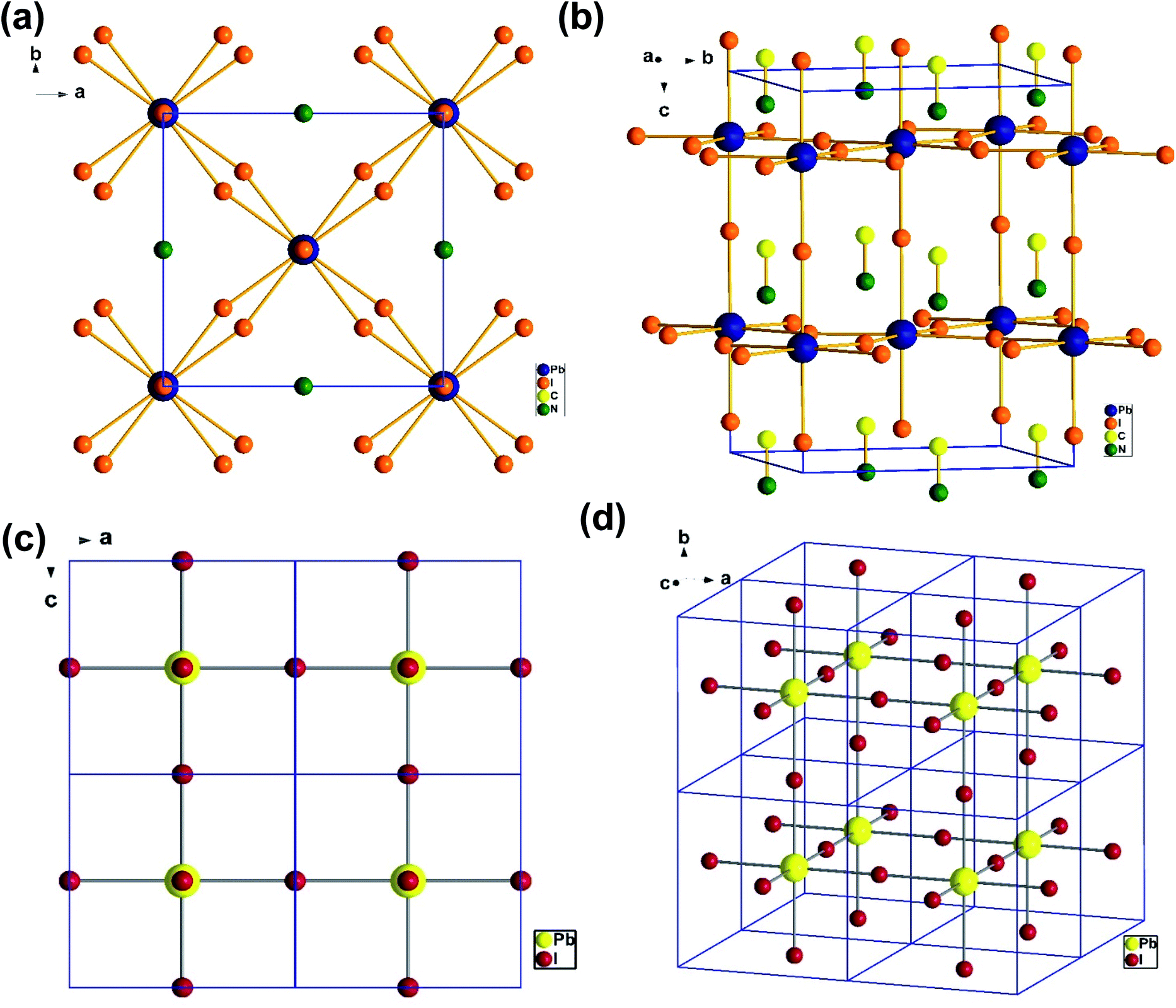
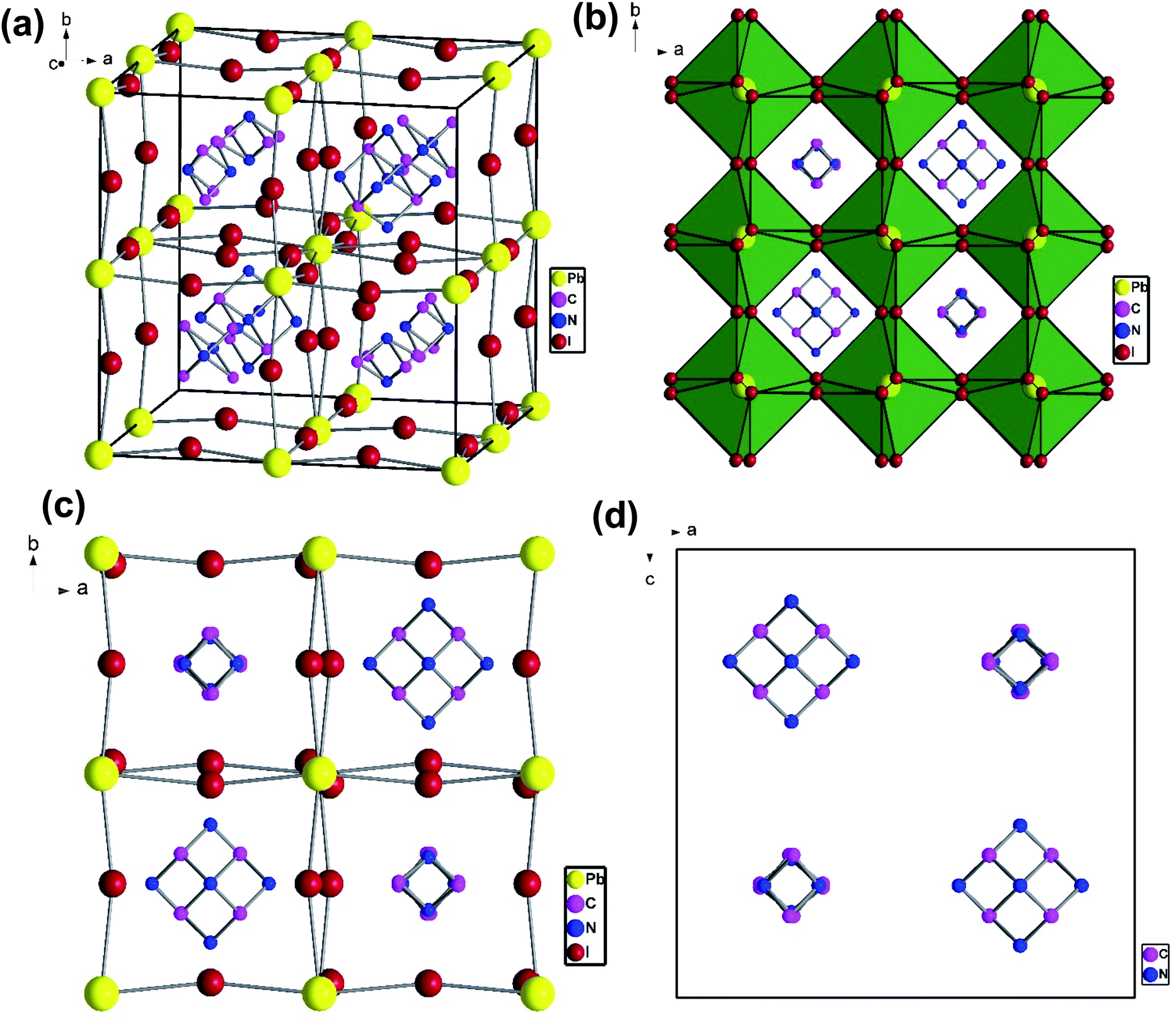
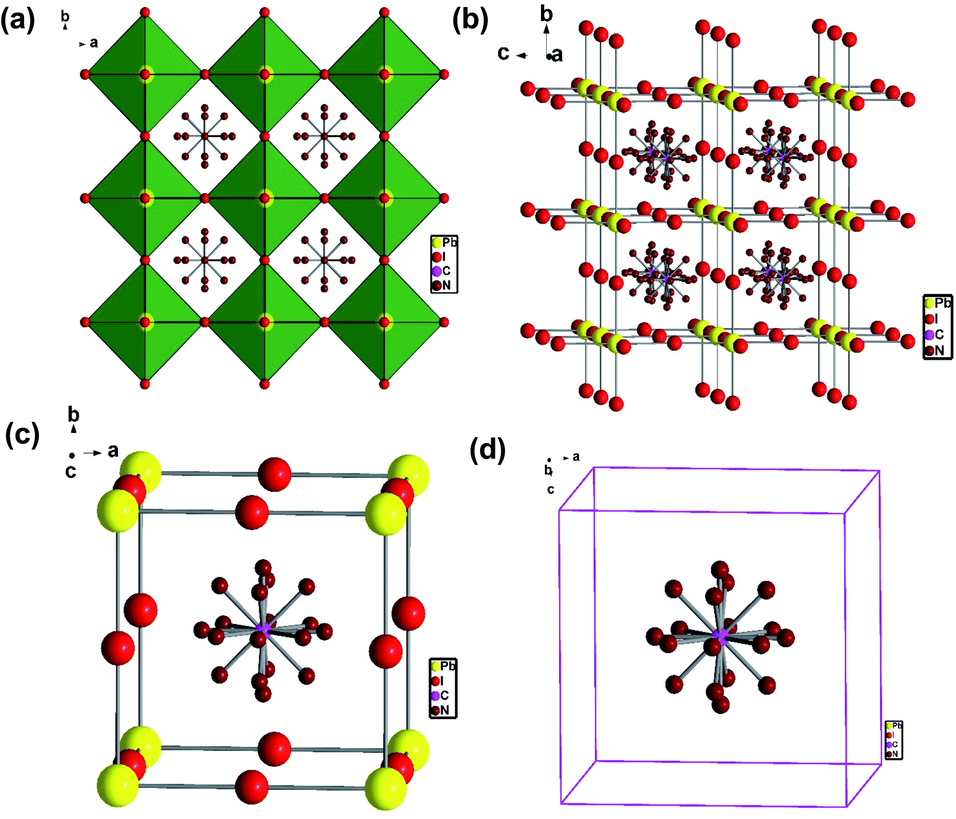
To understand the alloy phase of the MA0.5EA0.5PbI3 perovskite, a single crystal XRD measurement was performed to study the crystal structure, which could explain the mechanism of the inhibition of the phase transition with the alloy formation. As shown in Fig. 1c and d, the unit cell of MA0.5EA0.5PbI3 shows a cubic Pm![[3 with combining macron]](https://www.rsc.org/images/entities/char_0033_0304.gif) m space group with a = b = c = 6.3257(7) Å and a cell volume of 253.12(8) Å3. By comparing the unit cell parameters of MA0.5EA0.5PbI3 with those of the MAPbI3 and the EAPbI3, the unit cell volume of MA0.5EA0.5PbI3 was contracted from 990.3(3) Å3 and 1080.1(4) Å3 for the MAPbI3 (tetragonal and I4cm) and the EAPbI3 (orthorhombic and Pnma), which are illustrated in Fig. 1c and d, to 253.12(8) Å3. The lattice contraction of MA0.5EA0.5PbI3 can be probably attributed to the fact that with the introduction of two different cations, which are MA and EA, the disordering of cations was fully developed due to the change in the hydrogen bonding between the organic cation hydrogen atom and the iodide ion of the inorganic lattice. This is the hydrogen bonding disruption with a dissimilar hydrogen bonding strength, and the orientation and the acidity are illustrated by the FAxMA1−xPbI3 crystal structure,23 which reduces the octahedral volume of the A site cation that is surrounded by the PbI6 octahedra in the unit cell. This occurrence is mentioned by Xie et al.13 Therefore, the Goldschmidt tolerance factor (α)24 for this perovskite structure approaches 1, which is mostly found in the cubic perovskite. We introduced a ternary organic cation based perovskite to understand the cubic phase stabilization, which is essential for device stability. As shown in Fig. 2, the crystal structure of MA0.65FA0.3EA0.05PbI3 shows the cation disorder of MA+ and FA+ in the crystal. As a small amount of the EA+ cation was incorporated into the FAxMA1−xPbI3 crystal structure, the MA+ disorder in the unit cell was over 16 possible sites, but the FA+ disorder in the crystal was over 8 possible sites, which are illustrated in Fig. 2a–d. The MA0.65FA0.3BA0.05PbI3 perovskite shows the FA+ disorders in the crystal over 9 possible sites, which is illustrated in Fig. 3a–d. These results suggest that the incorporation of the cation plays an important role in cubic phase stabilization because it has a stronger dipole and more flexible orientation, which results in a high degree of cation disorder.13 According to the Goldschmidt tolerance factor, t, is defined as follows:
m space group with a = b = c = 6.3257(7) Å and a cell volume of 253.12(8) Å3. By comparing the unit cell parameters of MA0.5EA0.5PbI3 with those of the MAPbI3 and the EAPbI3, the unit cell volume of MA0.5EA0.5PbI3 was contracted from 990.3(3) Å3 and 1080.1(4) Å3 for the MAPbI3 (tetragonal and I4cm) and the EAPbI3 (orthorhombic and Pnma), which are illustrated in Fig. 1c and d, to 253.12(8) Å3. The lattice contraction of MA0.5EA0.5PbI3 can be probably attributed to the fact that with the introduction of two different cations, which are MA and EA, the disordering of cations was fully developed due to the change in the hydrogen bonding between the organic cation hydrogen atom and the iodide ion of the inorganic lattice. This is the hydrogen bonding disruption with a dissimilar hydrogen bonding strength, and the orientation and the acidity are illustrated by the FAxMA1−xPbI3 crystal structure,23 which reduces the octahedral volume of the A site cation that is surrounded by the PbI6 octahedra in the unit cell. This occurrence is mentioned by Xie et al.13 Therefore, the Goldschmidt tolerance factor (α)24 for this perovskite structure approaches 1, which is mostly found in the cubic perovskite. We introduced a ternary organic cation based perovskite to understand the cubic phase stabilization, which is essential for device stability. As shown in Fig. 2, the crystal structure of MA0.65FA0.3EA0.05PbI3 shows the cation disorder of MA+ and FA+ in the crystal. As a small amount of the EA+ cation was incorporated into the FAxMA1−xPbI3 crystal structure, the MA+ disorder in the unit cell was over 16 possible sites, but the FA+ disorder in the crystal was over 8 possible sites, which are illustrated in Fig. 2a–d. The MA0.65FA0.3BA0.05PbI3 perovskite shows the FA+ disorders in the crystal over 9 possible sites, which is illustrated in Fig. 3a–d. These results suggest that the incorporation of the cation plays an important role in cubic phase stabilization because it has a stronger dipole and more flexible orientation, which results in a high degree of cation disorder.13 According to the Goldschmidt tolerance factor, t, is defined as follows:  , where rA and rB are the ionic radius of the A and B site cations, respectively, and rx is the ionic radius of the anion.24,25 The perovskite structure can be predicted using a simple geometric consideration; for a 3D perovskite, the value of 0.8 ≤ t ≤ 1. A tolerance factor of t ≈ 1 results in the formation of a cubic perovskite structure, whereas lower t values result in a cubic structure of lower symmetry, such as tetragonal or orthorhombic. Herein, we calculated the tolerance factor for our compounds. The resultant values including the parameters are shown in Table S1 in the ESI.† The tolerance factors of MA0.67FA0.33PbI3, MA0.5FA0.5PbI3, MA0.83EA0.17PbI3, MA0.65FA0.3EA0.05PbI3, MA0.53FA0.38EA0.09PbI3, and MA0.65FA0.30BA0.05PbI3 perovskites are 0.9363, 0.9491, 0.9317, 0.9400, 0.9508, and 0.9653, respectively. The tolerance factors of all compounds indicate the 3D perovskite structure, consistent with the cubic phase in single crystal XRD measurement.
 |
| | Fig. 1 The crystal structure of MAPbI3 from the (a) top-down view along the b axis and (b) side view of the tetragonal unit cell. The crystal structure of MA0.5EA0.5PbI3 from the (c) a top-down view along the b axis and (d) a view of the cubic unit cell. | |
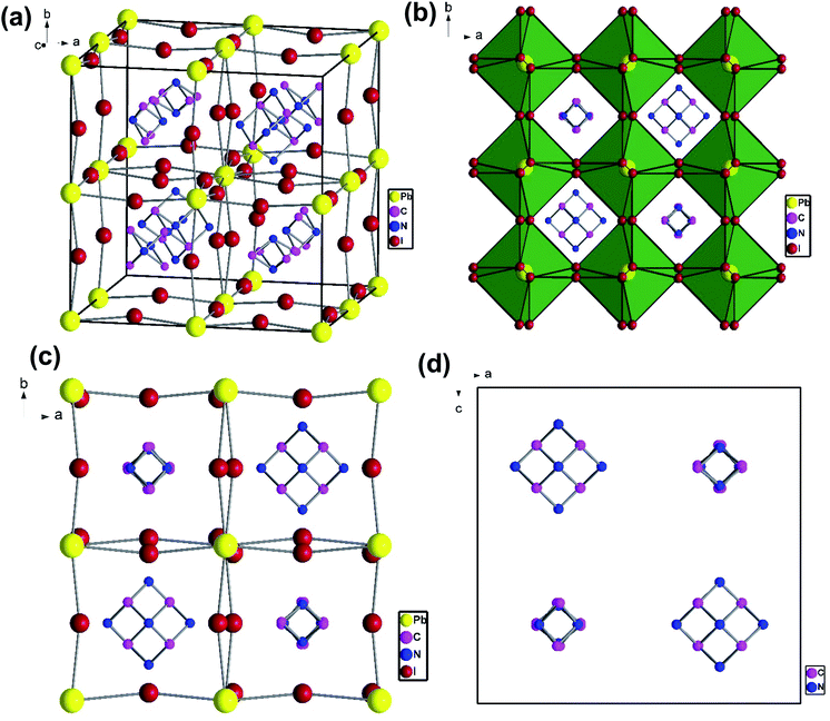 |
| | Fig. 2 The crystal structure of MA0.65FA0.3EA0.05PbI3 to show the cation disorder of MA+ and FA+ from (a) a side view of the cubic unit cell and (b–d) a top view along the c axis. | |
 |
| | Fig. 3 (a) The crystal structure of the MA0.65FA0.3BA0.05PbI3 perovskite, (b) the side view of the disordering of FA+, and (c, d) the disordering FA+ cation in a cubic unit cell. | |
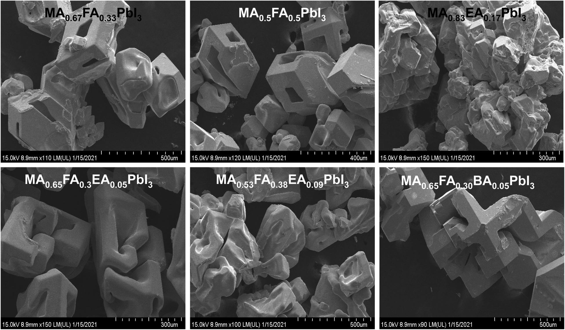
Fig. 4 shows the SEM images of alloy perovskite crystals with an irregular shape, indicating the formation of the alloy crystal rather than a perfect crystal phase. Especially, MA0.83EA0.17PbI3 shows an aggregated shape of the crystal phase. As a result, MA0.83EA0.17PbI3 thin film exhibits a very compact film, as shown in Fig. 10. The morphology of 2D perovskite films generally shows plate-like morphology because it reflects the crystal shape and orientation with 2D characteristics. In contrast, 3D perovskite film exhibits larger grain size and denser stacking in the perpendicular direction to the substrate in comparison with the 2D perovskite. This is attributed to the crystal orientation of the 3D perovskite phase. For example, Lian et al.26 found that larger colloidal size plays an important role in the formation of high quality film and large grains. Lv et al.27 showed that the film quality is affected by particle sizes of the aggregate of the precursor. Therefore, we speculate that the aggregate shape of the MA0.83EA0.17PbI3 crystal could induce the formation of high quality films.
 |
| | Fig. 4 The SEM images of single crystal of MA0.67FA0.33PbI3, MA0.5FA0.5PbI3, MA0.83EA0.17PbI3, MA0.65FA0.3EA0.05PbI3, MA0.53FA0.38EA0.09PbI3, and MA0.65FA0.30BA0.05PbI3 perovskites. | |
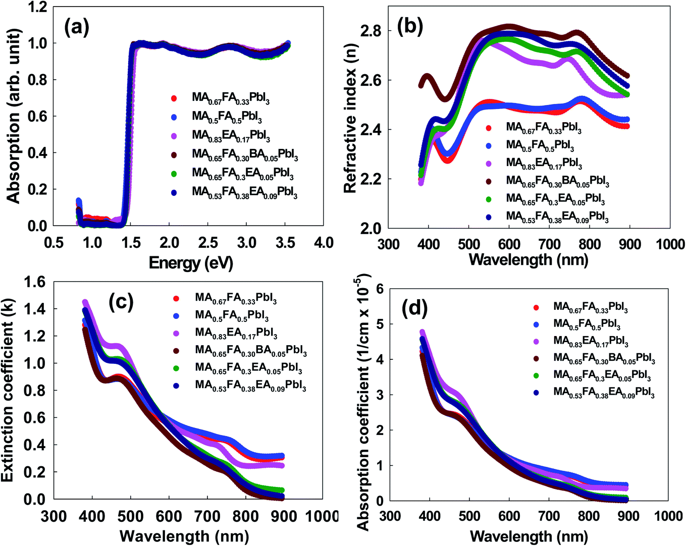
To assess the optical characteristics, we measured the absorption spectra, the optical constants (n and k), and the absorption coefficient for the perovskites. The absorption spectra, which are illustrated in Fig. 5a, are similar for all the perovskites. The band gap energies were determined to be 1.41 eV, 1.40 eV, 1.46 eV, 1.42 eV, 1.43 eV, and 1.42 eV for MA0.67FA0.33PbI3, MA0.5FA0.5PbI3, MA0.83EA0.17PbI3, MA0.65FA0.3EA0.05PbI3, MA0.53FA0.38EA0.09PbI3, and MA0.65FA0.30BA0.05PbI3 perovskites, respectively. This result indicates that the band gaps show only negligible difference because incorporated cations do not form the 2D perovskites, showing the same features as the 3D perovskite structure. The approach is attractive due to its suitable band gap for its derived perovskite solar cells and also can be applied to improve the phase stability successfully, as shown in Fig. 12b. This indicates that the optical properties were mainly governed by the inorganic perovskite part of the structure. The main difference comes from the distortion of the structure, which is represented by the Pb–I–Pb equatorial tilting angles. Herein, all the perovskites have cubic crystal structures, having the value of 180° in the Pb–I–Pb framework. This result reflected that insulating the organic layer has a negligible effect on the optical properties of mixed perovskite structures.28,29 The optical constants of perovskites, which are shown in Fig. 5b and c, were fitted based on the Gaussian oscillator, which used preferences to determine the band gap for the transparent organics, and the semiconductor materials because they allow a shorter absorption tail. The value of the refractive index (n) for each material had a shoulder at 440 nm with the lowest value, and it showed an approximately constant value from 500 nm to 800 nm in the entire visible region and then decreased in the IR region. Compared to FAxMA1−xPbI3 perovskites, the 2D perovskites that incorporated the 3D MA1−xFAxPbI3 perovskites showed higher n values. The value of the extinction coefficient (κ) of perovskites, which is the imaginary part of the refractive index, substantially decreases as a function of the wavelength. The absorption coefficients of all the perovskites showed a strong absorption above the band edge, which indicates direct band gap materials. This is illustrated in Fig. 5d.
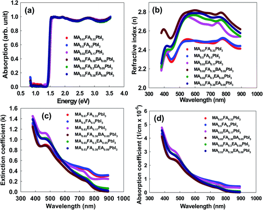 |
| | Fig. 5 (a) The UV-visible diffuse reflectance spectra, (b) the real, n, refractive index, (c) the imaginary, k, refractive index, and (d) the adsorption coefficient for 3D MAPbI3 and alloy perovskites. | |
As shown in Fig. 6, except for MA0.5EA0.17PbI3 perovskite, the powder XRD patterns of all the perovskites are similar to those of α-FAPbI3 with slightly enlarged diffraction angles caused by the MA+, BA+, and EA+ incorporation, which indicates the same cubic crystal phase as that of α-FAPbI3. In the previous reports,13,14 α-FAPbI3 was easily converted from a pristine α-phase to a non-perovskite β-phase due to its thermodynamically unstable structure. However, the cation incorporated α-FAPbI3 phase exhibits superior stability in ambient air as well as thermal stability that results from a thermodynamically stable structure and high crystallinity. We present the powder XRD patterns and simulated patterns from single crystal XRD for MA0.83EA0.17PbI3, MA0.65FA0.30BA0.05PbI3, and MA0.65FA0.3EA0.05PbI3 perovskites in Fig. S1 in the ESI.† The powder XRD patterns have almost the same features as the simulated patterns from the single crystal XRD. As shown in Fig. 6, except for MA0.83EA0.17PbI3, the perovskites, the powder XRD patterns of all the perovskites are similar to those of α-FAPbI3 because it show cubic crystal structures. However, MA0.83EA0.17PbI3 without FA has poor crystallinity and shows a different crystal structure compared to other perovskites. The MA0.83EA0.17PbI3 compound is an alloy of 3D MAPbI3 and 1D EAPbI3 (EAPbI3 is crystallized to a long chain-like 1D structure, which consists of only face-sharing PbI6), not the 2D layered structures ((EA)2(MA)n−1PbnI3n+1). Thus, since the XRD pattern of MA0.83EA0.17PbI3 reflects the property of the alloy compound, 1D EAPbI3, and 3D MAPbI3 perovskite structures, we speculate that the intensity of the diffraction is weak compared to other alloy perovskites.
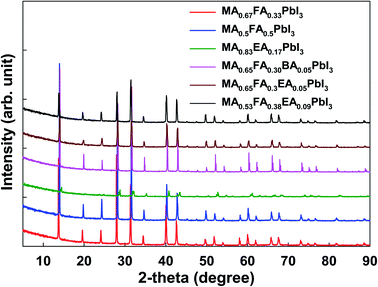 |
| | Fig. 6 The powder X-ray diffraction of 3D MAPbI3 and the alloy perovskites. | |
As shown in Fig. 7, we measured the TRPL in order to study the kinetics of the excitons and the free carriers in the mixed perovskites. The TRPL profiles were fitted with three exponential decays, and the detailed fitting parameters are listed in Table 1. The decay component, τ1, is assigned to the non-radiative recombination by the trap states of the perovskite crystal structure, and the decay processes (τ2 and τ3) corresponded to the radiative recombination from the bulk perovskite.30,31 As shown in Table 1, the MAPbI3 exhibits 0.43 ns (41.67%), 1.82 ns (48.33%), and 3.83 ns (10.00%) for τ1, τ2, and τ3, respectively. Except for the MA0.67FA0.33PbI3 and the MA0.83EA0.17PbI3 perovskites, the PL lifetimes of all the perovskites were predominantly determined by the τ1 component, because the values of A1 are in the range of 85.75% to 98.68%, and the MA0.67FA0.33PbI3 and the MA0.83EA0.17PbI3 perovskites represent an A2 that is 23.16% for τ2 = 2.74 and A2 of 30.15% for τ2 = 2.13, respectively. In this respect, these perovskites showed much more efficient exciton recombination, which results in a decrease in the generation of free carriers compared to other perovskites. As a consequence, all of these situations have shown that the PL lifetimes of the alloyed perovskites do not improve significantly compared to the 3D perovskite, MAPbI3. It was observed that there were decreases in the MA0.5FA0.5PbI3, the MA0.65FA0.3EA0.05PbI3, and the MA0.53FA0.38EA0.09PbI3 perovskites, which are illustrated in Fig. 7a. Except for the MA0.65FA0.30BA0.05PbI3, the image mapping of PL lifetimes, which is illustrated in Fig. 7b, indicates that the alloyed perovskites have a short carrier lifetime compared to that of MAPbI3.
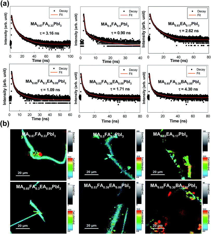 |
| | Fig. 7 (a) The transient photoluminescence decay profile of single crystal MA0.67FA0.33PbI3, MA0.5FA0.5PbI3, MA0.83EA0.17PbI3, MA0.65FA0.3EA0.05PbI3, MA0.53FA0.38EA0.09PbI3, and MA0.65FA0.30BA0.05PbI3 perovskites at room temperature. The fitting results, which are the solid curves, were also included for comparison. (b) The image mapping of the emission decay of the MA0.67FA0.33PbI3, MA0.5FA0.5PbI3, MA0.83EA0.17PbI3, MA0.65FA0.3EA0.05PbI3, MA0.53FA0.38EA0.09PbI3, and MA0.65FA0.30BA0.05PbI3 perovskite single crystals. | |
Table 1 Photoluminescence lifetime results of 3D alloy perovskites from the transient photoluminescencea
| Perovskites |
A1/% |
τ1/ns |
A2/% |
τ2/ns |
A3/% |
τ3/ns |
τ/ns |
τamp/ns |
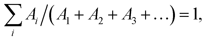
The emission decay was analyzed using the equation: I(t) = A1exp(−t/τ1) + A2exp(−t/τ2) + A3exp(−t/τ3) + …, where  the average lifetime, 〈τ〉, is defined by the average lifetime, 〈τ〉, is defined by 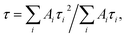 and τamp is the amplitude of average lifetime. and τamp is the amplitude of average lifetime. |
| MAPbI3 |
41.67 |
0.43 |
48.33 |
1.82 |
10.00 |
3.83 |
2.18 |
1.43 |
| MA0.67FA0.33PbI3 |
74.52 |
0.77 |
23.16 |
2.74 |
2.31 |
10.00 |
3.16 |
1.44 |
| MA0.5FA0.5PbI3 |
98.68 |
0.25 |
1.14 |
2.00 |
0.18 |
9.10 |
0.90 |
0.29 |
| MA0.83EA0.17PbI3 |
65.79 |
0.63 |
30.15 |
2.13 |
4.06 |
6.80 |
2.62 |
1.33 |
| MA0.65FA0.3EA0.05PbI3 |
89.65 |
0.34 |
9.82 |
1.31 |
0.52 |
6.80 |
1.09 |
0.47 |
| MA0.53FA0.38EA0.09PbI3 |
86.82 |
0.40 |
12.58 |
1.56 |
0.60 |
9.90 |
1.71 |
0.60 |
| MA0.65FA0.30BA0.05PbI3 |
85.75 |
0.32 |
12.64 |
2.10 |
1.61 |
13.00 |
4.30 |
0.74 |
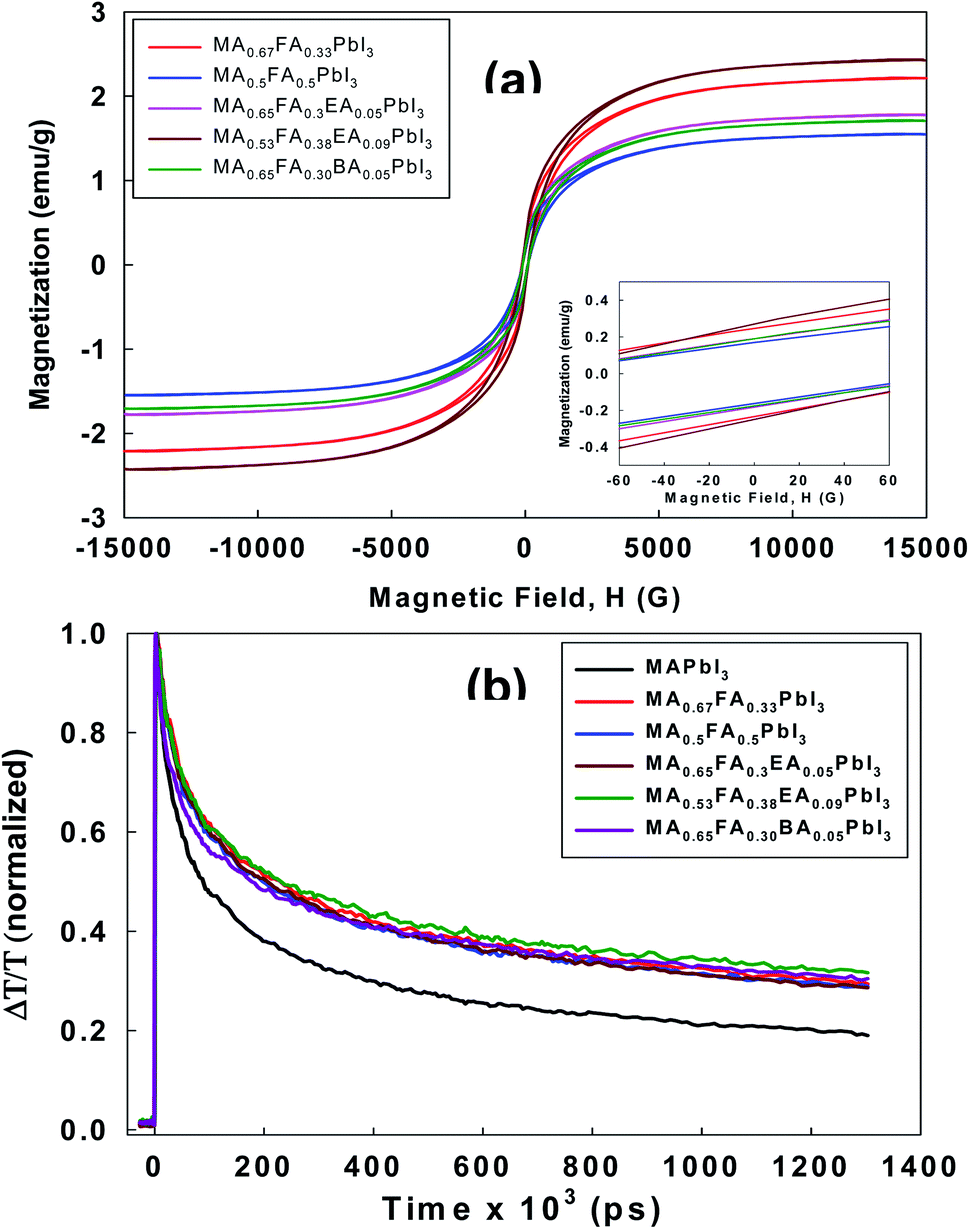
All the perovskites in this study showed a cubic crystal structure, which is a very highly symmetric crystal system. However, previous reports32 found that twining was observed in MAPbI3 as an intrinsic functionality regardless of changes in the composition. This is often commonly observed in the transformation from the high symmetry phase to the low symmetry phase, which is also called the cubic phase to the tetragonal phase. These features have a significant impact on optical properties. In particular, the perovskite layer is composed of a tiny crystalline domain, and natural disordering is the driving force to produce the relatively long-lived spin-1/2 electron–hole pairs.33 Thus, the generation and the recombination of the exciton may be influenced by a magnetic field. In consideration of this, we performed the measurement of magnetic properties for the alloy perovskites using VSM. As shown in Fig. 8a, all the perovskites showed a clear paramagnetic response. This paramagnetism is related to the unique crystal orientation of alloy perovskites. According to the related hysteresis loops in Fig. 8a, the coercivity (Hci) is 114.57 Oe, 98.546 Oe, 102.10 Oe, 101.06 Oe, and 101.13 Oe for MA0.67FA0.33PbI3, MA0.5FA0.5PbI3, MA0.65FA0.3EA0.05PbI3, MA0.53FA0.38EA0.09PbI3, and MA0.65FA0.30BA0.05PbI3 perovskites, respectively. The remnant magnetization (Mr) is in the range of 0.16 to 0.27 emu g−1, which indicates a soft ferromagnetic behavior. As a matter of fact, the alloy perovskites are far away from the related values of superparamagnetics with no hysteresis. However, the crystal orientation, the anisotropy, and the crystal size distribution have the potential to change the M − H hysteresis curve.
 |
| | Fig. 8 (a) The magnetic hysteresis curves of the MA0.67FA0.33PbI3, MA0.5FA0.5PbI3, MA0.65FA0.3EA0.05PbI3, MA0.53FA0.38EA0.09PbI3, and MA0.65FA0.30BA0.05PbI3 perovskites measured using VSM at room temperature. The inset is the low-field portion that shows the HC values. (b) Charge carrier dynamics measured with optical pump-THz probe spectroscopy. The wavelength of the pump beam is 400 nm with the intensity of 40 μJ cm−2. The THz time domain signals were collected in the spectral range from 0.2 to 2.5 THz. | |
To investigate the optoelectronic properties of these alloy perovskites, we measured the effective charge-carrier mobility in thin films using the optical pump-THz probe spectroscopy. The wavelength of the pump beam is 400 nm with an intensity of 40 μJ cm−2. The THz time domain signals were collected in the spectral range from 0.2 to 2.5 THz. Upon photoexcitation, the fractional change in THz amplitude (ΔT/T) was measured as a function of the time delay between the optical pump pulse and THz probe pulse. The ΔT/T signal can be changed into the photoinduced conductivity, which corresponds to the product of the carrier density and the mobility, μ.34 Since these experiments do not contain the fraction φ of adsorbed photons that is changed into free charge-carrier pairs, the effective mobility, φμ, can be calculated. Generally, because the excitonic effect of 3D perovskite can be negligible at room temperature, φ = 1, the effective charge mobility is regarded as the actual mobility. As shown in Fig. 8b, compared to 3D MAPbI3 perovskite, the mobilities of all alloy perovskites were enhanced. This suggests that cubic structures of alloy perovskites have improved the orientation and are perpendicular to the substrate and thus show higher mobility than 3D perovskite. To assess the effectiveness of carrier transport, we measured the mobility of alloy perovskites using the hall effect measurement. The calculated carrier mobility is 8.02, 17.52, 14.71, 25.87, 19.02, 15.60 and 14.87 cm2 V−1 s−1 for MAPbI3, MA0.67FA0.33PbI3, MA0.5FA0.5PbI3, MA0.83EA0.17PbI3, MA0.65FA0.3EA0.05PbI3, MA0.53FA0.38EA0.09PbI3, and MA0.65FA0.30BA0.05PbI3 perovskites, respectively. The mobility of the 3D MAPbI3 perovskite is similar to that of the previous 3D MAPbI3 thin films, which exhibit the charge-carrier mobility in the range of from 1 to 11.6 cm2 V−1 s−1 (ref. 33) and it was improved to 36.0 cm2 V−1 s−1 by the thermal annealing process.34 Compared to 3D MAPbI3 perovskite film, the alloy perovskite films display increased mobility due to the higher charge carrier concentration and conductivity, as mentioned in Fig. 8b. That is, the defect density in alloy perovskite films was reduced compared to control film, MAPbI3, resulting in the enhancement in photo-carrier transport.
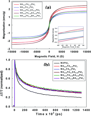
The adequate energy band structure of the perovskites between the conduction band minimum (CBM) and the valence band minimum (VBM) is important to make the charge extraction efficient from the perovskites and to facilitate the electron/hole transport in the photovoltaic application. The electronic structure of 2D perovskites was studied by UPS, which is illustrated in Fig. 9. For each compound, the top panel shows the UPS survey spectra and the homo level states, which are shown in Fig. 9a and b. The bottom panel shows the photoemission cut-off, from which the work function of the surface is extracted, and it is displayed in Fig. 9c. Even though the VBM is determined from the first ionization energy at low binding energy, the position of the CBM relative to the vacuum level (Evac) was estimated from the difference between the optical band gap and the VBM position.35,36 All the energies are referenced to a common Fermi level (EF) of the Au substrate (0 eV). Fig. 9d shows the alignment of the energy level of the alloy perovskite series when it was applied into an FTO/TiO2/perovskite/Spiro-MeOTAD/Au solar cell configuration. The 3D MA1−xFAxPbI3 perovskites exhibited the VBM energy closer to the highest occupied molecular orbital (HOMO) level of the HTL, which indicated that there was no hole extraction barrier. However, the EA cation and the BA cation incorporated into the MA1−xFAxPbI3 perovskites showed a larger barrier compared to MA1−xFAxPbI3 perovskites. The lowest unoccupied molecular orbital (LUMO) level of the HTL is positioned above the CBM of perovskites, which indicates a large barrier to prevent electron loss at the interface between the perovskites and the HTL layer. Since the HOMO level of the HTL was in a position 100 meV lower than the perovskite VBM, the built-in field and the collection of the hole were constrained, which caused the Voc to decrease from the device point of view. As shown in Fig. 9d, the deeper CBM of MA0.83EA0.17PbI3 perovskite film can reduce the recombination possibility of electrons from the perovskite with the hole in the HTL layer, which is beneficial to the enhancement of Voc, whereas the gap between the VBM of MA0.83EA0.17PbI3 and the HOMO level of HTL is large compared to the other film, which would become the barrier of hole extraction at the perovskite/HTL interface. However, the film morphology of the MA0.83EA0.17PbI3 perovskite film shows the most packed and uniform film among perovskites (Fig. 10). Thus, the highest efficiency in MA0.83EA0.17PbI3 based device was achieved compared to the other perovskite devices (Table 2). This indicates that both the intrinsic and physical properties of the films affect the device performance.
 |
| | Fig. 9 The micro X-ray/UV photoelectron spectrometer characterization for the alloy perovskites/FTO substrate. (a) The wide binding energy range valence spectra, (b) the narrow binding energy range valence spectra, (c) the secondary-electron cutoffs for the work function determination, and the (d) energy level of the 3D MAPbI3 and the alloy perovskites for the FTO/TiO2/perovskite/Spiro-MeOTAD/Au solar cell configuration. | |
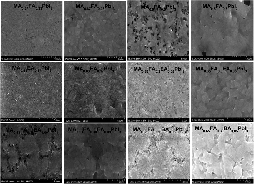 |
| | Fig. 10 Low and high resolution scanning electron microscopy (SEM) images of MA0.67FA0.33PbI3, MA0.5FA0.5PbI3, MA0.83EA0.17PbI3, MA0.65FA0.3EA0.05PbI3, MA0.53FA0.38EA0.09PbI3, and MA0.65FA0.30BA0.05PbI3 perovskite films. | |
Table 2 The champion photovoltaic parameters of solar cells using 3D MAPbI3 and alloy perovskites based on FTO/compact TiO2/mesoporous TiO2/perovskite/Spiro-MeOTAD/Au
| Perovskites |
Jsc [mA cm−2] |
Voc [V] |
FF [%] |
η [%] |
| MAPbI3 |
17.01 |
1.00 |
58.23 |
9.89 |
| MA0.67FA0.33PbI3 |
16.98 |
0.84 |
65.71 |
9.34 |
| MA0.5FA0.5PbI3 |
18.76 |
0.94 |
47.13 |
8.27 |
| MA0.83EA0.17PbI3 |
16.28 |
0.99 |
63.45 |
10.22 |
| MA0.65FA0.3EA0.05PbI3 |
14.00 |
0.84 |
63.01 |
7.38 |
| MA0.53FA0.38EA0.09PbI3 |
11.96 |
0.87 |
48.97 |
5.07 |
| MA0.65FA0.30BA0.05PbI3 |
12.93 |
0.87 |
64.62 |
7.29 |
The morphology of the perovskite alloy films is shown in Fig. 10. The SEM image of MAPbI3 (Fig. S2†) shows dendritic crystalline aggregates in several places. However, the MA0.67FA0.33PbI3, MA0.83EA0.17PbI3, and MA0.65FA0.3EA0.05PbI3 perovskite films display a compact polycrystalline grain texture and a pinhole-free morphology that fully cover the MP-TiO2 substrate. With the MA0.53FA0.38EA0.09PbI3 and MA0.65FA0.30BA0.05PbI3 perovskite films, it was observed that there were some pinholes in the films, which is more severe in the MA0.5FA0.5PbI3 perovskite film. This result is well consistent with the lowest fill factor in MA0.5FA0.5PbI3 perovskite based devices, as shown in Fig. 12. In addition, this suggests that the precursor solution of these perovskites should make a highly supersaturated concentration, which exists with a large number of uniformly distributed nuclei in the precursor solution.37
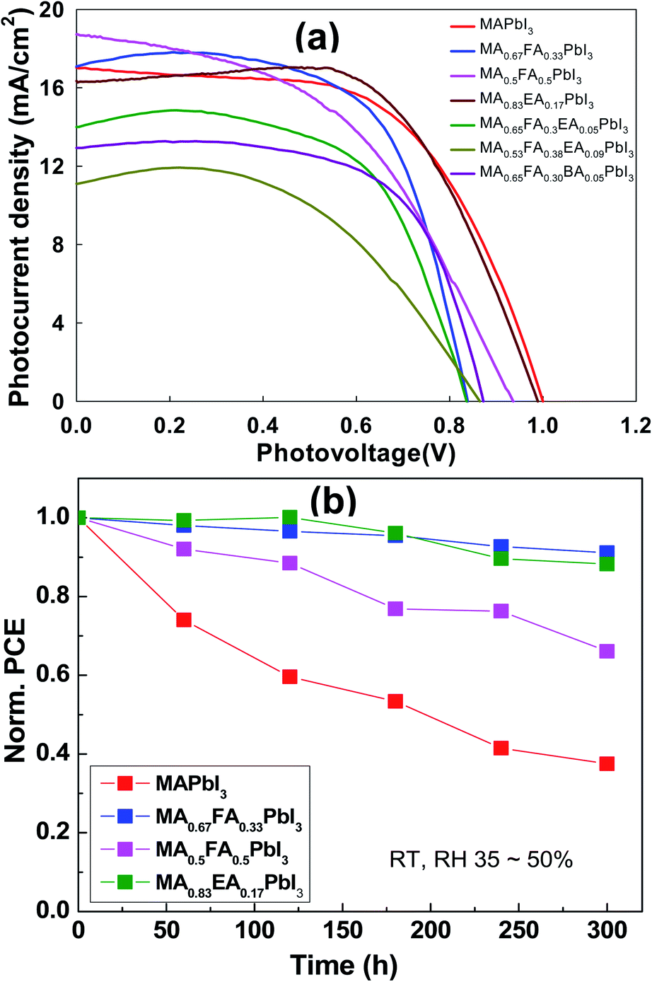
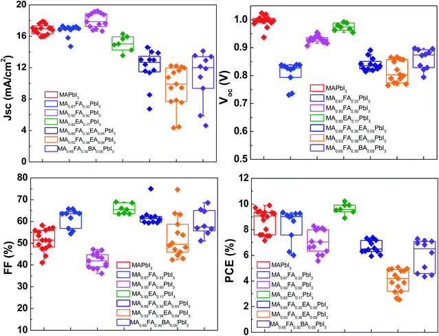
The planar devices were fabricated with n–i–p PSCs with a configuration of FTO/blocking TiO2/meso-TiO2/3D or an alloy perovskite layer/Spiro-OMeTAD/Au. The PSC distributions of MAPbI3 and alloy perovskite based devices are displayed in Fig. 11. The MAPbI3 cells achieved an average PCE 8.67 ± 0.93% with a Voc of 1.00 ± 0.02 V, Jsc of 16.87 ± 0.65 mA cm−2, and an FF of 51.56 ± 4.94%. The MA0.67FA0.33PbI3 and MA0.5FA0.5PbI3 cells show a comparable Jsc, 16.69 ± 0.82 mA cm−2 and 18.02 ± 0.96 mA cm−2, respectively, to the MAPbI3 cells, however these devices have a much lower average Voc of 0.81 ± 0.04 V for MA0.67FA0.33PbI3 and FF of 41.96 ± 3.59% for MA0.5FA0.5PbI3 to the MAPbI3 cells, resulting in average PCE 8.36 ± 1.28% and 7.06 ± 0.94%, respectively. The Jsc (15.08 ± 0.97 mA cm−2) and Voc (0.97 ± 0.01%) of MA0.83EA0.17PbI3 devices is lower than that of MAPbI3 cells. But, it exhibits significantly improved FF, 65.67 ± 2.32%, compared to MAPbI3, resulting in an improved PCE of 9.64 ± 0.43%. The MA0.65FA0.3EA0.05PbI3, MA0.53FA0.38EA0.09PbI3, and MA0.65FA0.30BA0.05PbI3 cells show improved FF, 62.32 ± 4.65%, 52.78 ± 9.37%, and 59.47 ± 6.04%, respectively, compared to MAPbI3. However, Jsc and Voc of these cells show less than that of MAPbI3, yielding PCE of 6.65 ± 0.51%, 4.06 ± 0.87%, and 5.99 ± 1.23%, respectively. The Jsc–Voc curves of the champion cells are presented in Fig. 12a, and the photovoltaic parameters are summarized in Table 2. The MA0.83EA0.17PbI3 perovskite cell presented a champion PCE of 10.22% along with Jsc of 16.28 mA cm−2, Voc of 0.99 V and FF of 63.45%, which is ascribed to the formation of higher quality perovskites with a low defect density favorable to the carrier transport. Long-term stability of alloy perovskite devices was investigated under ambient conditions (35–50% RH and 25 ± 3 °C). As shown in Fig. 12b, significant degradation of performances was observed in the 3D MAPbI3 device over 300 h with 62.48% of its initial PCE (from 9.89% to 3.71%). Whereas MA0.67FA0.33PbI3, MA0.5FA0.5PbI3, and MA0.83EA0.17PbI3 perovskites retains 91.12%, 66.08%, and 88.24% of their original PCE after 300 h. This result indicates that the migration of ions in alloy perovskites is inhibited to prevent degradation of the perovskite, thereby increasing the stability of the perovskite cell due to the increase in coulombic interactions between space cations existing in the 3D structure.
 |
| | Fig. 11 The photovoltaic performance, which is the J–V curve obtained from a forward scan, of the alloy perovskite solar cells made with regular structure (FTO/TiO2 BL/TiO2 MP/alloy perovskites/Spiro-OMeTAD) under simulated AM (air mass) 1.5 G (global) illumination (100 mW cm−2). | |
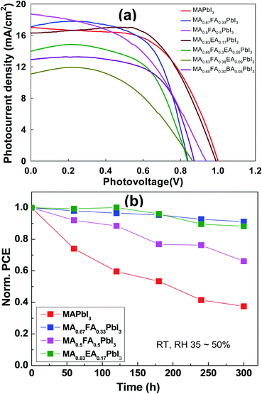 |
| | Fig. 12 (a) The photovoltaic performance, which is the J–V curve obtained from the alloy perovskite solar cells made with regular structure (FTO/TiO2 BL/TiO2 MP/alloy perovskites/Spiro-OMeTAD) under simulated AM (air mass) 1.5 G (global) illumination (100 mW cm−2). (b) The stability test of unencapsulated MAPbI3 and alloy perovskites devices at room temperature and a relative humidity condition of 35–50%. | |
4. Conclusions
We have presented the alloy 3D perovskites with the incorporation of EA and BA cations into the 3D MA1−xFAxPbI3 perovskites within the range that did not form the 2D perovskite phase. The incorporation of the cation plays an important role in the cubic phase stabilization because if it has a stronger dipole and more flexible orientation, it will result in a high degree of cation disorder. The alloy perovskites showed much more efficient exciton recombination, which decreased the generation of a free carrier compared to other perovskites. As a consequence, all of these situations have shown that the PL lifetimes of the alloyed perovskites do not improve significantly compared to the 3D perovskite, which is the MAPbI3. All the alloy perovskites are far away from the related values of the superparamagnetics with no hysteresis. However, crystal orientation, anisotropy, and the crystal size distribution have the potential to change the M − H hysteresis curve. In the regular solar cell, n–i–p, the PCE of the MA0.83EA0.17PbI3 perovskite solar cell shows the highest efficiency of 10.22% under 1 sun illumination.
Conflicts of interest
There are no conflicts to declare.
Acknowledgements
This research was supported by the Basic Science Research Program through the National Research Foundation of Korea (NRF), funded by the Ministry of Education (2016R1D1A1B04931751). This work was supported by the National Research Foundation of Korea (NRF) grant funded by the Korean government (MSIT) (2019R1A2C1003108). This research was supported by Nano Material Technology Development Program through the National Research Foundation of Korea (NRF) funded by the Ministry of Science, ICT, and Future Planning (2009-0082580).
References
- T. M. Koh, K. Fu, Y. Fang, S. Chen, T. C. Sum, N. Mathews, S. G. Mhaisalkar, P. P. Boix and T. Baikie, J. Phys. Chem. C, 2014, 118, 16458–16462 CrossRef CAS.
- Q. Han, S.-H. Bae, P. Sun, Y.-T. Hsieh, Y. Yang, Y. S. Rim, H. Zhao, Q. Chen, W. Shi, G. Li and Y. Yang, Adv. Mater., 2016, 28, 2253–2258 CrossRef CAS PubMed.
- M. T. Weller, O. J. Weber, J. M. Frost and A. Walsh, J. Phys. Chem. Lett., 2015, 6, 3209–3212 CrossRef CAS.
- F. Ma, J. Li, W. Li, N. Lin, L. Wang and J. Qiao, Chem. Sci., 2017, 8, 800–805 RSC.
- N. J. Jeon, J. H. Noh, W. S. Yang, Y. C. Kim, S. Ryu, J. Seo and S. I. Seok, Nature, 2015, 517, 476 CrossRef CAS PubMed.
- D. P. McMeekin, G. Sadoughi, W. Rehman, G. E. Eperon, M. Saliba, M. T. Hörantner, A. Haghighirad, N. Sakai, L. Korte, B. Rech, M. B. Johnston, L. M. Herz and H. J. Snaith, Science, 2016, 351, 151–155 CrossRef CAS PubMed.
- K. Yan, M. Long, T. Zhang, Z. Wei, H. Chen, S. Yang and J. Xu, J. Am. Chem. Soc., 2015, 137, 4460–4468 CrossRef CAS PubMed.
- L. N. Quan, M. Yuan, R. Comin, O. Voznyy, E. M. Beauregard, S. Hoogland, A. Buin, A. R. Kirmani, K. Zhao, A. Amassian, D. H. Kim and E. H. Sargent, J. Am. Chem. Soc., 2016, 138, 2649–2655 CrossRef CAS PubMed.
- H. Tsai, W. Nie, J.-C. Blancon, C. C. Stoumpos, R. Asadpour, B. Harutyunyan, A. J. Neukirch, R. Verduzco, J. J. Crochet, S. Tretiak, L. Pedesseau, J. Even, M. A. Alam, G. Gupta, J. Lou, P. M. Ajayan, M. J. Bedzyk, M. G. Kanatzidis and A. D. Mohite, Nature, 2016, 536, 312 CrossRef CAS PubMed.
- R. Yang, R. Li, Y. Cao, Y. Wei, Y. Miao, W. L. Tan, X. Jiao, H. Chen, L. Zhang, Q. Chen, H. Zhang, W. Zou, Y. Wang, M. Yang, C. Yi, N. Wang, F. Gao, C. R. McNeill, T. Qin, J. Wang and W. Huang, Adv. Mater., 2018, 30, 1804771 CrossRef PubMed.
- M. I. Saidaminov, A. L. Abdelhady, B. Murali, E. Alarousu, V. M. Burlakov, W. Peng, I. Dursun, L. Wang, Y. He, G. Maculan, A. Goriely, T. Wu, O. F. Mohammed and O. M. Bakr, Nat. Commun., 2015, 6, 7586 CrossRef PubMed.
- L. Chen, Y.-Y. Tan, Z.-X. Chen, T. Wang, S. Hu, Z.-A. Nan, L.-Q. Xie, Y. Hui, J.-X. Huang, C. Zhan, S.-H. Wang, J.-Z. Zhou, J.-W. Yan, B.-W. Mao and Z.-Q. Tian, J. Am. Chem. Soc., 2019, 141, 1665–1671 CrossRef CAS PubMed.
- L.-Q. Xie, L. Chen, Z.-A. Nan, H.-X. Lin, T. Wang, D.-P. Zhan, J.-W. Yan, B.-W. Mao and Z.-Q. Tian, J. Am. Chem. Soc., 2017, 139, 3320–3323 CrossRef CAS PubMed.
- W.-G. Li, H.-S. Rao, B.-X. Chen, X.-D. Wang and D.-B. Kuang, J. Mater. Chem. A, 2017, 5, 19431–19438 RSC.
- J. W. Shin, K. Eom and D. Moon, J. Synchrotron Radiat., 2016, 23, 369–373 CrossRef PubMed.
- Z. Otwinowski and W. Minor, in Methods in Enzymology, Academic Press, New York, 1997, vol. 276 Search PubMed.
- G. M. Sheldrick, Acta Crystallogr., Sect. A: Found. Crystallogr., 2015, 71, 3–8 CrossRef PubMed.
- G. M. Sheldrick, Acta Crystallogr., Sect. C: Cryst. Struct. Commun., 2015, 71, 3–8 CrossRef PubMed.
- K. Chondroudis, T. J. McCarthy and M. G. Kanatzidis, Inorg. Chem., 1996, 35, 840–844 CrossRef CAS PubMed.
- T. J. McCarthy and M. G. Kanatzidis, Inorg. Chem., 1995, 34, 1257–1267 CrossRef CAS.
- J. Park, C. Kim, J. Lee, C. Yim, C. H. Kim, J. Lee, S. Jung, J. Ryu, H.-S. Kang and T. Joo, Rev. Sci. Instrum., 2011, 82, 013305 CrossRef PubMed.
- H.-S. Kim, J.-W. Lee, N. Yantara, P. P. Boix, S. A. Kulkarni, S. Mhaisalkar, M. Grätzel and N.-G. Park, Nano Lett., 2013, 13, 2412–2417 CrossRef CAS PubMed.
- O. J. Weber, B. Charles and M. T. Weller, J. Mater. Chem. A, 2016, 4, 15375–15382 RSC.
- G. Kieslich, S. Sun and A. K. Cheetham, Chem. Sci., 2014, 5, 4712–4715 RSC.
- W. Travis, E. N. K. Glover, H. Bronstein, D. O. Scanlon and R. G. Palgrave, Chem. Sci., 2016, 7, 4548–4556 RSC.
- X. Lian, J. Chen, M. Qin, Y. Zhang, S. Tian, X. Lu, G. Wu and H. Chen, Angew. Chem., Int. Ed., 2019, 58, 9409–9413 CrossRef CAS PubMed.
- G. Lv, L. Li, D. Lu, Z. Xu, Y. Dong, Q. Li, Z. Chang, W.-J. Yin and Y. Liu, Nano Lett., 2021, 21, 5788–5797 CrossRef CAS PubMed.
- E. P. Booker, T. H. Thomas, C. Quarti, M. R. Stanton, C. D. Dashwood, A. J. Gillett, J. M. Richter, A. J. Pearson, N. J. L. K. Davis, H. Sirringhaus, M. B. Price, N. C. Greenham, D. Beljonne, S. E. Dutton and F. Deschler, J. Am. Chem. Soc., 2017, 139, 18632–18639 CrossRef CAS PubMed.
- C. Quarti, N. Marchal and D. Beljonne, J. Phys. Chem. Lett., 2018, 9, 3416–3424 CrossRef CAS PubMed.
- L. Mao, H. Tsai, W. Nie, L. Ma, J. Im, C. C. Stoumpos, C. D. Malliakas, F. Hao, M. R. Wasielewski, A. D. Mohite and M. G. Kanatzidis, Chem. Mater., 2016, 28, 7781–7792 CrossRef CAS.
- X. Wu, M. T. Trinh, D. Niesner, H. Zhu, Z. Norman, J. S. Owen, O. Yaffe, B. J. Kudisch and X. Y. Zhu, J. Am. Chem. Soc., 2015, 137, 2089–2096 CrossRef CAS PubMed.
- M. U. Rothmann, W. Li, Y. Zhu, U. Bach, L. Spiccia, J. Etheridge and Y.-B. Cheng, Nat. Commun., 2017, 8, 14547 CrossRef CAS PubMed.
- C. Wehrenfennig, G. E. Eperon, M. B. Johnston, H. J. Snaith and L. M. Herz, Adv. Mater., 2014, 26, 1584–1589 CrossRef CAS PubMed.
- R. L. Milot, R. J. Sutton, G. E. Eperon, A. A. Haghighirad, J. Martinez Hardigree, L. Miranda, H. J. Snaith, M. B. Johnston and L. M. Herz, Nano Lett., 2016, 16, 7001–7007 CrossRef CAS PubMed.
- A. Kahn, Mater. Horiz., 2016, 3, 7–10 RSC.
- P. Schulz, E. Edri, S. Kirmayer, G. Hodes, D. Cahen and A. Kahn, Energy Environ. Sci., 2014, 7, 1377–1381 RSC.
- F. Huang, Y. Dkhissi, W. Huang, M. Xiao, I. Benesperi, S. Rubanov, Y. Zhu, X. Lin, L. Jiang, Y. Zhou, A. Gray-Weale, J. Etheridge, C. R. McNeill, R. A. Caruso, U. Bach, L. Spiccia and Y.-B. Cheng, Nano Energy, 2014, 10, 10–18 CrossRef CAS.
Footnote |
| † Electronic supplementary information (ESI) available. See DOI: 10.1039/d1ra04520b |
|
| This journal is © The Royal Society of Chemistry 2021 |
Click here to see how this site uses Cookies. View our privacy policy here. 
 Open Access Article
 This Open Access Article is licensed under a Creative Commons Attribution-Non Commercial 3.0 Unported Licence
 *
*
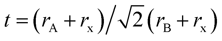 , where rA and rB are the ionic radius of the A and B site cations, respectively, and rx is the ionic radius of the anion.24,25 The perovskite structure can be predicted using a simple geometric consideration; for a 3D perovskite, the value of 0.8 ≤ t ≤ 1. A tolerance factor of t ≈ 1 results in the formation of a cubic perovskite structure, whereas lower t values result in a cubic structure of lower symmetry, such as tetragonal or orthorhombic. Herein, we calculated the tolerance factor for our compounds. The resultant values including the parameters are shown in Table S1 in the ESI.† The tolerance factors of MA0.67FA0.33PbI3, MA0.5FA0.5PbI3, MA0.83EA0.17PbI3, MA0.65FA0.3EA0.05PbI3, MA0.53FA0.38EA0.09PbI3, and MA0.65FA0.30BA0.05PbI3 perovskites are 0.9363, 0.9491, 0.9317, 0.9400, 0.9508, and 0.9653, respectively. The tolerance factors of all compounds indicate the 3D perovskite structure, consistent with the cubic phase in single crystal XRD measurement.


 the average lifetime, 〈τ〉, is defined by
 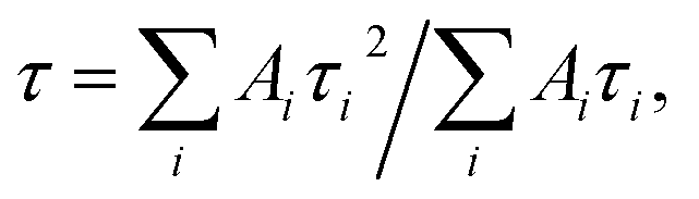 and τamp is the amplitude of average lifetime.