
 Open Access Article
 This Open Access Article is licensed under a Creative Commons Attribution-Non Commercial 3.0 Unported Licence
Impact of synthesis conditions on the morphology and crystal structure of tungsten nitride nanomaterials
Olivia Wenzel *a,
Viktor Reinb,
Milena Hugenschmidtac,
Frank Schillingd,
Claus Feldmannb and
Dagmar Gerthsena
*a,
Viktor Reinb,
Milena Hugenschmidtac,
Frank Schillingd,
Claus Feldmannb and
Dagmar Gerthsena
aLaboratory for Electron Microscopy (LEM), Karlsruhe Institute of Technology (KIT), Engesserstr. 7, 76131 Karlsruhe, Germany. E-mail: Olivia.Wenzel@kit.edu
bInstitute for Inorganic Chemistry (AOC), Karlsruhe Institute of Technology (KIT), Engesserstr. 15, 76131 Karlsruhe, Germany
c3DMM2O – Cluster of Excellence (EXC-2082/1 – 390761711), Karlsruhe Institute of Technology (KIT), 76131 Karlsruhe, Germany
dInstitute of Applied Geosciences (AGW), Karlsruhe Institute of Technology (KIT), Adenauerring 20b, 76131 Karlsruhe, Germany
First published on 20th August 2021
Abstract
Nanocrystalline tungsten nitride (WNx) aggregates and nanosheets are synthesized with a new alkylamine-based synthesis strategy for potential applications in nanoelectronics and catalysis. These applications preferentially require crystalline materials with controlled morphology, which has been rarely demonstrated for WNx nanomaterials in the past. In the synthesis approach presented in this work, the morphology of nanoscale WNx is controlled by long-chained amines that form lyotropic or lamellar phases depending on the surfactant concentration. The structural and chemical properties of the WNx nanomaterials are studied in detail using different electron microscopic techniques in combination with electron spectroscopic analyses. Material synthesis and sample preparation for transmission electron microscopy (TEM) were performed in an argon atmosphere (Schlenk line and glovebox). The samples were inserted into the electron microscope via an air-tight TEM transfer holder to protect the material from hydrolysis and oxidation. From the lyotropic phase nanocrystalline WNx aggregates were obtained, which consist of 2.4 ± 0.8 nm small crystallites of the cubic WNx phase with a composition of WN0.7. The lamellar phase with a higher surfactant concentration yields WNx nanosheets with lateral dimensions up to 500 nm and a mean thickness of 2.1 ± 1.1 nm. The nanosheets are N rich with a composition WN1.7–3.7 and occur in the hexagonal crystal structure. The nanosheets are often stacked on top of one another with frequent rotations of 4–6° around the hexagonal c axis, thereby forming commensurate interface structures between nanosheets. High stacking-fault densities and signs of nanotwins can be repeatedly observed in WNx nanosheets.
1. Introduction
Two-dimensional (2D) nanomaterials consisting merely of a few atomic planes, denoted as sheets in the following, have sparked considerable attention from multiple research fields due to their exotic material properties. Most publications are dedicated to graphene, hexagonal boron nitride, and transition metal dichalcogenides not only due to their interesting properties but also because of their ease of syntheses.1–5 Their bulk counterparts already display a crystal structure composed of atomic layers with strong in-plane bonds and lower binding energies between the layers, which allows easy exfoliation and delamination of individual sheets. Conversely, thin 2D sheets of materials that do not have a preferential internal layered structure are more challenging to synthesize and are, hence, only sporadically described in the literature. However, it seems likely that materials which have suitable material properties in bulk-form would display interesting properties as 2D materials, too. One class of such materials relates to transition metal nitrides with members such as tungsten nitride (WNx). Most common in the W–N system is the cubic β-WNx phase with space group Fm![[3 with combining macron]](https://www.rsc.org/images/entities/char_0033_0304.gif) m and lattice parameter a = 4.13 Å. The cubic β-phase is stable at nitrogen concentrations of about 30–50 at%.6 For nitrogen concentrations of 50 at% and above, only phases with hexagonal and trigonal crystal structures occur. The δ-WNx phase is characterized by the space group P
m and lattice parameter a = 4.13 Å. The cubic β-phase is stable at nitrogen concentrations of about 30–50 at%.6 For nitrogen concentrations of 50 at% and above, only phases with hexagonal and trigonal crystal structures occur. The δ-WNx phase is characterized by the space group P![[6 with combining macron]](https://www.rsc.org/images/entities/char_0036_0304.gif) 2m and lattice parameters a = 2.89 Å and c = 2.83 Å. Further derivative structures (δ1, δ2) and a nitrogen-rich cubic structure (β1) are compiled in Table 1.6,7
2m and lattice parameters a = 2.89 Å and c = 2.83 Å. Further derivative structures (δ1, δ2) and a nitrogen-rich cubic structure (β1) are compiled in Table 1.6,7
| Phase | Crystal structure | Space group | Lattice parameters | Ref. |
|---|---|---|---|---|
| β-WN0.5–1 | Cubic | Fmm |
a = 4.13 Å | COD 1538664 (Khitrova, 1959)8 |
| β1-W3N4 | Cubic | Pmm |
a = 4.13 Å | ICSD 186209 (Wang et al., 2012)7 |
| δ-WN0.66–2 | Hexagonal | Pm2 |
a1,2 = 2.89 Å, c = 2.83 Å | COD 1539264 (Schoenberg, 1954)9 |
| δ1-W2N3 | Hexagonal | P63/mmc | a1,2 = 2.89 Å, c = 15.29 Å | ICSD 186207 (Wang et al., 2012)7 |
| δ1-W5N4 | Hexagonal | P63/mmc | a1,2 = 2.89 Å, c = 15.30 Å | COD 1540231 (Khitrova, Pinsker 1958)10 |
| δ2-W2N3 | Trigonal | R3:H | a1,2 = 2.89 Å, c = 15.29 Å | ICSD 186208 (Wang et al., 2012)7 |
| δ2-WN2 | Trigonal | Rm:H |
a1,2 = 2.89 Å, c = 23.35 Å | COD 1541851 (Khitrova 1962)11 |
Reversible reactions between the β and the δ phases have so far not been observed. Between 33 and 50 at% N, both phases can coexist as a phase mixture, which has been experimentally shown by Schönberg.9 Other observed phases comprise the δ1-W2N3 and δ2-W2N3 phases, which were obtained by high-pressure synthesis.7
In bulk form, WNx phases are mechanically very stable as they have a high hardness, good electrical conductivity and show resistance to chemical deterioration, which is in part related to low diffusion rates of, e.g., Cu in the structure.12–14 Because of this slow diffusion, WNx can be used as a diffusion barrier between copper and Si in microelectronics.15,16 In view of the ongoing development from microelectronics to nanoelectronics, the realization of homogeneous and high-purity nitride nanomaterials has seen an increase in attention in the last years.17 Furthermore, nanosized WNx is of interest in the field of catalysis, since the addition of N atoms to the metal structure serves as chemical functionalization, thereby giving the metal electronic and catalytic properties of noble metals.18–21 WNx can replace costly Pt-based catalysts in various redox-reactions,22–24 oxygen-reduction reactions and hydrogen evolution reactions in fuel cells.15,25–28 Further, heterostructures based on WNx were shown to have a highly efficient electrocatalytical performance comparable to Pt-based materials in experimental studies by Diao et al.27 Such catalytic materials require a high surface area, which can be achieved with a nanoporous material structure composed of aggregated nanometer-sized crystallites or a material made up of nanosheets. Similarly, various 2D MXene materials are being investigated as catalyst replacements in these electrochemical reactions.29,30 However, their low structural stability and the use of toxic HF in the synthesis can be seen as disadvantageous for realistic commercial production compared to WNx nanomaterials.30 Another interesting application of nanostructured WNx with a nanosheet morphology could be as nanofillers in polymer-based nanocomposites, where the good electrical conductivity of WNx can be used to improve the material properties of the whole composite material.2,31–33
The preparation of transition metal nitride nanomaterials is hampered by the high temperatures in conventional approaches (>600 °C), which is why most studies and applications of WNx are limited to bulk material.34 Moreover, the vulnerability of transition metal nitrides towards material-deteriorating hydrolysis and oxidation reactions is exacerbated when aiming at nanosized materials.35,36 Hence, there are only few reports on WNx nanomaterials, especially with regard to nanosheets, compared to extensive work on their oxide equivalents. Wang et al. have very recently produced WNx nanosheets on Si–SiO2 substrates by salt-assisted chemical vapor deposition by reacting WO3 and NaCl powders with NH3 at 800 °C.37 This method produces 3 nm thin WNx layers with a thicker nucleus in the middle. Yu et al.38 have grown epitaxial hexagonal W2N3 on (002) KCl surfaces during ammonolysis of an oxygen and H2O-based tungsten precursor, which produces stacks of nanosheets. Jin et al. first synthesize a sodium tungsten oxide intermediate product that already has a 2D geometry and ammonolysed it, which resulted in a mixture of Na2WO4 and W2N3 nanosheets.39 However, the use of oxygen-containing compounds in the aforementioned syntheses is considered to be disadvantageous due to oxide contaminants in the final product. Further, the methods of Wang et al.37 and Jin et al.39 require additional processing after synthesis to isolate the WNx nanosheets.
Our work focuses on the synthesis and in-depth characterization of the structural and chemical properties of two WNx nanomaterials, namely nanocrystalline aggregates consisting of condensed nanoparticles (batch a) and nanosheets (batch b). Both were obtained with an alkylamide-assisted synthesis in the liquid phase, which avoids the use of any oxygen-containing compounds. The morphology of the material (nanocrystalline aggregates or nanosheets) can be controlled by the concentration of long-chained amine surfactants under otherwise identical synthesis conditions. Nanocrystalline aggregates were obtained with a lyotropic phase formed by self-assembly of long-chained amine surfactants. At higher surfactant concentrations, a lamellar phase promotes parallel growth and results in the formation of WNx nanosheets. In addition, the adjustment of the surfactant concentration results in a change in nitrogen concentration in the final nanomaterial, which in turn impacts the crystal structure. A higher surfactant concentration in the synthesis implies more abundant nitrogen for the reaction and an increase in nitrogen in the final nitride. As previously described, lower nitrogen concentrations are stabilized in the cubic phase, whereas higher nitrogen concentrations are stabilized in the hexagonal phase.6 Several transmission electron microscopy (TEM) techniques including analytical techniques (energy-dispersive X-ray spectroscopy: EDXS and electron energy loss spectroscopy: EELS) were used to study the structural and chemical properties on the nanoscale. Essential for this work was the material synthesis and TEM sample preparation in an argon atmosphere (Schlenk line and glovebox) as well as an air-tight transfer TEM holder to protect the material from oxidation and hydrolysis.
2. Materials and methods
2.1 Material synthesis
The synthesis of aggregated WNx nanoparticles (batch a): 83 mg of WCl6 (0.22 mmol) as the starting material and 621 mg of lithiumbutylamide (Li-HNBu) (7.8 mmol) as the surfactant were added to 15 mL of heptane as the non-polar oil-phase (cf. Fig. 1(a)). This suspension was stirred for two days. In this time, WCl6 reacts with Li-HNBu to form W(HNBu)x and LiCl as a colorless precipitate (Fig. 1(b)). Butylamine serves as soft-template and forms micelles around W(HNBu)x (Fig. 1(c)). In the last step, the solution was evaporated and heated to 800 °C in N2 atmosphere in order to react W(HNBu)x to WNx. Therefore, the final material structure was dominated by evaporation-induced self-assembly.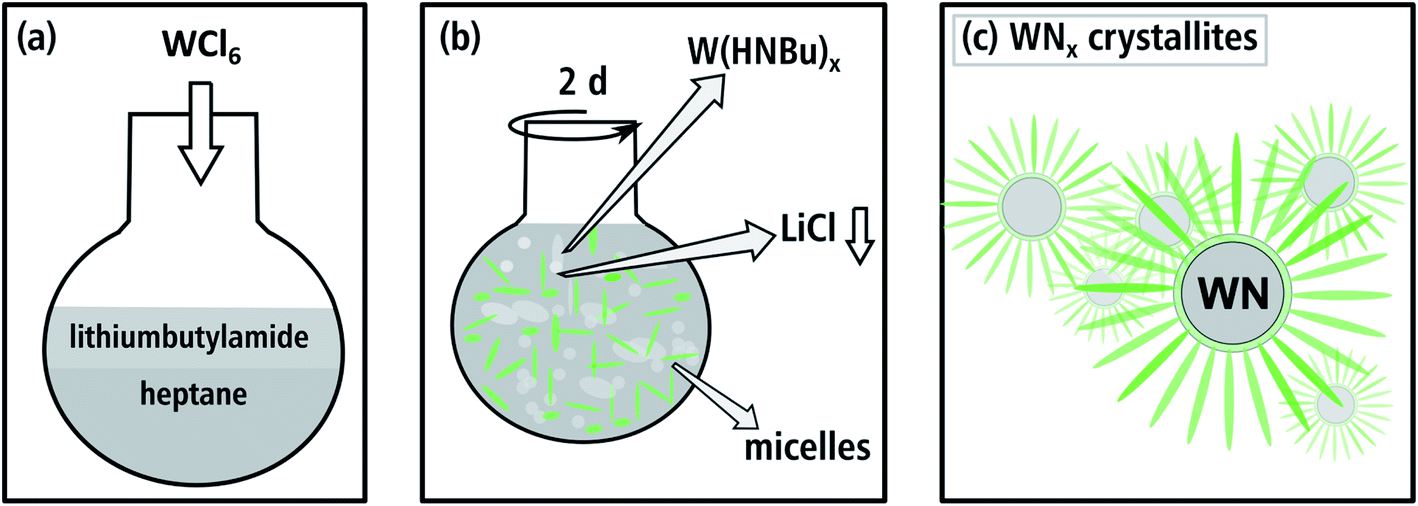 | ||
| Fig. 1 Illustration of the synthesis route for batch a in (a) and (b), where W(HNBu)x and a micellar template are formed. (c) The soft sacrificial template produces small aggregated WNx crystallites. | ||
To obtain a nanosheet morphology of WNx (batch b) similar synthesis conditions were used as described for batch a (cf. Fig. 2(a)). The predominant differences in batch b relate to a higher concentration and the longer chain-length of the surfactant. Thus, 550 mg of lithiumheptylamide (Li-HNHep) (4.6 mmol) and 300 mg of WCl6 (0.8 mmol) were added to a solution of 6 mL heptylamine (40.5 mmol) in 15 mL of heptane. Due to the higher concentration of heptylamide/heptylamine, a liquid-crystalline phase with a lamellar structure was formed by self-assembly (cf. Fig. 2(b)) instead of the aforementioned micellar system. This lamellar template forces the intermediate product W(HNHep)x and the final WNx to grow laterally, which is schematically depicted in Fig. 2(c). In the last step, the solution was evaporated and heated to 800 °C in N2 atmosphere to complete the ammonolysis and to react W(HNHep)x to WNx.
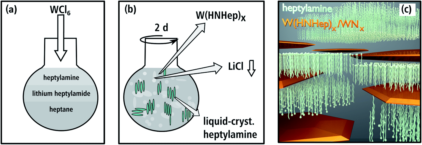 | ||
| Fig. 2 Illustration of the synthesis route for batch b in (a) and (b), where W(HNHep)x and a liquid-crystalline phase is formed. (c) Shows a model of the lateral crystal growth mechanism of W(HNHep)x and WNx. | ||
2.2 Sample preparation
Sample synthesis and preparation for TEM are a critical aspect as past analyses of related nanoscaled nitrides have shown high reactivity of the material with water or oxygen.40,41 Exposure to the ambient atmosphere swiftly results in deleterious reactions of the nitrides to form hydroxides and oxides. Therefore, sample synthesis was performed in Schlenk lines with Argon. For sample preparation for electron microscopy, the material was pipetted from a chloroform suspension onto conventional amorphous carbon lacy grids (Ultrathin C Film on Holey Carbon Support Film, CU 400 mesh from Plano, Prod No. 01824) in a Schlenk flask and transported in the Ar-filled flask to the glovebox (Ar inert gas). In the glovebox, the sample was deposited in an air-tight transfer holder and inserted into the microscope. This holder has a retractable lance with a rubber seal at the front tip, which preserves the sample in the Ar atmosphere of the glovebox.2.3 Analytical techniques
The structural properties of the materials were analyzed by TEM, high-angle annular dark-field scanning transmission electron microscopy (HAADF-STEM) and selected area electron diffraction (SAED) with Philips CM200 and Osiris Tecnai ChemiSTEM (formerly FEI, now Thermo Fisher Scientific) transmission electron microscopes operated at 200 kV. High-resolution (HR)TEM was performed with an FEI Titan3 80-300 operated at 300 kV that is equipped with an aberration corrector in the imaging lens system. Investigations regarding the surface morphology were performed with correlative bright-field (BF-)STEM and secondary-electron scanning electron microscopy (SE-SEM) imaging using a through-the-lens detector and a multi-segmented STEM detector in a focused-ion-beam (FIB)/SEM dual-beam Thermo Fisher Helios G4 FX operated at 30 kV.EDXS for chemical analysis was performed with an FEI Osiris ChemiSTEM microscope at 200 kV with an implemented Super-X system comprising four silicon drift detectors. Quantification of the EDXS spectra was carried out with the Bruker software package Esprit version 1.9. Element concentrations were calculated based on a refined Kramers' law model, which includes corrections for detector absorption and background subtraction. Standard-less quantification, i.e. by means of theoretical sensitivity factors, without thickness correction was applied. Element maps of the samples were acquired and used to determine the average chemical composition of homogeneous regions of interest. EELS was applied to analyze the energy loss near edge structure (ELNES) of the C–K edge to obtain information on the crystallinity of carbon contamination. For this purpose, a post-column Tridiem 865 HR Gatan imaging filter (GIF) was used that is attached at the Titan3 80-300 transmission electron microscope. Cumulative STEM-EELS spectra were taken over several seconds to gain spectra with sufficient signal-to-noise ratios. Spectra were measured with a spectrometer acceptance semi angle of 6.7 mrad (GIF aperture of 2.5 μm) and with an electron-beam convergence semi angle of 17.0 mrad at a camera length of 91 mm.
Crystallite sizes are given as circle diameter, which was calculated from measurements of the respective projected particle areas. The width of the sheets was measured from HAADF-STEM and HRTEM images at regions where the sheets were oriented perpendicular to the image plane. Whether a sheet was perpendicular or not was verified by the fringe distance, which has to correspond to the (001) lattice-plane distance. The crystal structure was analyzed using Fourier-transformed (FT) images calculated from HRTEM images with ImageJ.42 The generated FT patterns were indexed with Miller indices of crystal structures in the corresponding zone-axis orientation based on simulated diffraction patterns using JEMS.43
Debye SAED patterns were azimuthally integrated, background subtracted and displayed as radial intensity plots. All structure files used for indexing of the radial intensity plots were sourced from either the inorganic crystal structure database (ICSD) or the crystallography open database (COD).
3. Experimental results
3.1 Structural properties
WNx (batch a) consists of loosely aggregated crystallites, which vary in size between 320 nm up to 1.2 μm. The HAADF-STEM image in Fig. 3(a) shows a comparatively small aggregate on an amorphous carbon-film support. The latter appears with dark contrast due to its small thickness and low atomic number Z compared to the WNx aggregate. Fig. 3(b) taken with higher magnification shows that the nanometer-sized crystallites with irregular shapes form a nanoporous substructure. Particles establishing this substructure have sizes between 0.8 and 7.6 nm, with the majority of particles in a narrow size range of 1.6–3.2 nm and a mean size of 2.4 ± 0.8 nm.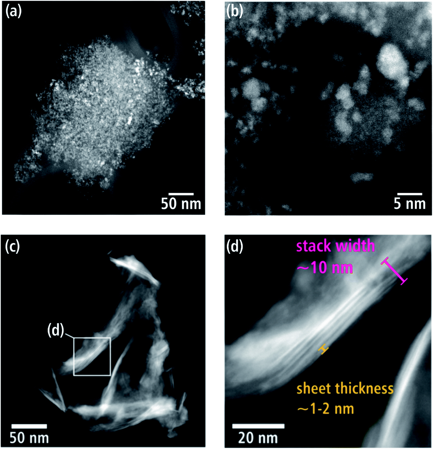 | ||
| Fig. 3 (a) HAADF-STEM overview image of a WNx aggregate (batch (a) and (b)) image taken at larger magnification. (c) HAADF-STEM overview of WNx nanosheets (batch (b)). The region indicated with a white square is shown enlarged in (d). A stack of nanosheets with a thickness of 1–2 nm is marked in (d). | ||
Batch b exhibits a completely different morphology. The HAADF-STEM image (Fig. 3(c)) shows an agglomerate of nanosheets. Some regions display a bright contrast with sometimes stripe-like appearance (e.g. region marked with a frame in Fig. 3(c)), which consist of stacked sheets (red mark in Fig. 3(d)) with a thickness of 1–2 nm. Such thin sheets occur frequently and statistical analysis of 143 measurements of sheet thicknesses reveals thicknesses between 0.7 and 4.9 nm with a predominance in the 1.8–2.9 nm range. The average sheet thickness is 2.1 ± 1.1 nm. Generally, WNx nanosheets are characterized by large extensions in two directions whereas their thickness is limited to a few atomic planes. These nanosheets can be stacked on top of one another, and stacks of sheets can be agglomerated as shown in Fig. 3(c). However, single stacks of sheets or even single sheets are frequently observed. Single sheets have a wide range of lateral sizes in contrast to their narrow thickness range. There are a few smaller sheets, which can be described as platelets with only tens of nanometers in lateral width amongst the majority of larger sheets, which extend up to 500 nm.
An example of a large sheet with a length of approximately 450 nm is shown in Fig. 4. The BF-STEM image (Fig. 4(a)) shows contrast inhomogeneities within the sheet and on the lacey film, which can be partially attributed to contaminations. The SE-SEM image (Fig. 4(b)), which is sensitive towards topography, reveals irregular dark and bright features on the nanosheet. Darker features are highlighted in some regions with a blue-green line. The bright rims surrounding the dark region (close-up in Fig. 4(c)) suggest that they are indeed on the surface of the nanosheet. The reason as to why they have a darker contrast despite being above WNx could be the atomic-number and material density dependency of SE imaging. Although SE contrast is typically ascribed to topological effects, there is an increase of SE yield with increasing atomic number between 1–20.44 Therefore, it is likely that these darker regions in Fig. 4(b) are residual surfactants, which were utilized to template the nanosheet.
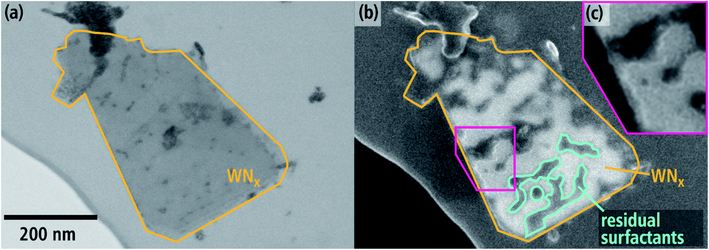 | ||
| Fig. 4 WNx nanosheet with several inhomogeneities visible in (a) BF-STEM and (b) SE-SEM images taken from the same region at 30 keV in a scanning electron microscope. (c) Shows a magnified region of (b). | ||
In the following, results of crystal structure and high-resolution TEM analyses of batch a and batch b will be comparatively presented.
Fig. 5(a) is an HRTEM image taken at the thin edge of a nanoporous WN aggregate of batch a with several individual crystallites. Two crystallites in Fig. 5(a) are marked with yellow and pink boxes and their FT is displayed in Fig. 5(b and c). The reflections can be indexed by assuming the cubic NaCl-type crystal structure of β-WNx (Fmm, a = 4.13 Å (ref. 8)) along the [112] and [011] zone axes.
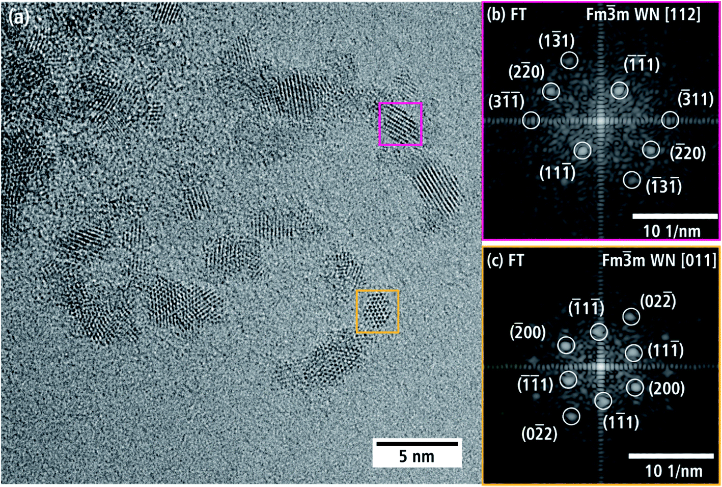 | ||
| Fig. 5 (a) HRTEM image of a thin region of a WNx aggregate with two crystallites (yellow and pink box) and their Fourier transforms in (b and c), which can be indexed with the cubic β-WNx crystal structure. | ||
A SAED pattern of an aggregate (batch a) is shown in Fig. 6(a), which is representative for the crystal structure of a large number of crystallites. The SAED pattern shows Debye rings with a diffuse appearance owing to the small coherent scattering domain sizes as already observed in Fig. 3(a and b). The intensities of the SAED pattern in Fig. 6(a) are azimuthally integrated and displayed as intensity profile over the spatial frequency in Fig. 6(b) after subtraction of the diffuse background. It shows four peaks at 4.93, 6.77, 7.95 and 10.61 nm−1, which can be indexed with the (002), (022), (113) and (133) reflections of the Fmm β-WN structure.8 The weak peaks at higher spatial frequencies in the profile can also be attributed to reflections of this crystal structure. The reflection at 4.19 nm−1 cannot be seen in Fig. 6(b), because it is covered by the beam stop (cf. Fig. 6(a)). We note that the cubic structure is clearly distinguishable from hexagonal δ-WNx. The intensities of the reflections in Fig. 6(b) reasonably agree with the expected kinematic intensities (pink lines in Fig. 6(b)) of the β-WN structure. The cubic WNx phase is the dominant phase of the material since it not only describes the two crystallites in Fig. 5(b and c) but also all Debye rings in the SAED pattern in Fig. 6. Tungsten oxides can be distinguished from both the cubic β-WNx structure as well as the hexagonal δ-WN since there are no oxide isostructures. In the case of tungsten carbides, there is one Fmm isostructure with close lattice parameters a = 4.13 Å.45 However, an EELS analysis presented in Section 3.2 will give arguments why a significant fraction of crystalline carbides cannot be present in this material.
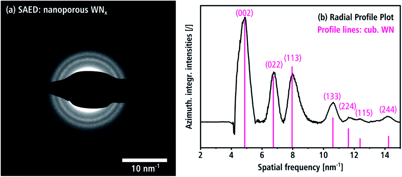 | ||
| Fig. 6 (a) SAED pattern of a nanocrystalline WNx aggregate with beam stop superimposed on the zero-order beam. The intensities of the Debye rings were azimuthally integrated and (b) plotted as a function of the spatial frequency. The pink lines indicate the calculated positions and kinematic intensities of the Bragg reflections for the β-WNx structure. | ||
Fig. 7(a) shows a single WNx sheet from batch b bordering a region with agglomerated sheets marked by * in the left part of the particle. The crystal structure of this sheet was examined by HRTEM (Fig. 7(b)) and FT analysis of the HRTEM image in Fig. 7(c). The HRTEM image shows a hexagonal pattern with atomic columns of alternating light and darker intensities. The corresponding FT image in Fig. 7(c) can be indexed with the hexagonal δ-WN crystal structure with space group Pm2 with a1,2 = 2.89 Å, c = 2.83 Å (COD 1539264) by Schönberg et al.9 in [001] zone-axis orientation. In this zone axis, the (001) planes consist of alternating W and N atomic columns in a hexagonal arrangement (cf. Fig. 7(d)). W and N are not in the same (001) plane but are offset by 0.5 c along the hexagonal c-axis and rotated by 60° around the c-axis. The δ-WN phase is stable as a monophase at 50 at% N.6 We note that the δ-WN phase cannot be distinguished from the δ1-W2N3, δ2-W2N3 and δ2-WN2 phases in this zone-axis orientation.
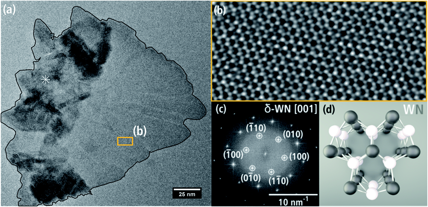 | ||
| Fig. 7 (a) Bright-field TEM image of a sheet aggregate (left side) bordering a single WNx sheet and (b) HRTEM image from the region of the single sheet marked in (a). (c) Shows the FT of (b) and is indexed with the hexagonal δ-WNx structure. A model of this crystal structure in [001] zone-axis orientation is shown in (d). | ||
SAED confirms the presence of the hexagonal δ-WN crystal structure of the nanosheets. In Fig. 8(a) numerous Bragg reflections with various intensities are visible, which suggests a pronounced crystallinity. The intensity of the SAED pattern is displayed as azimuthally integrated intensity as a function of the spatial frequency in Fig. 8(b) after subtraction of the diffuse background. All peaks in the radial intensity plot can be all indexed with reflections of the hexagonal δ-WN crystal structure with space group Pm2 (COD 1539264) and lattice parameters a1,2 = 2.89 Å and c = 2.83 Å by Schönberg et al.9 Reflections for the nitrogen-rich hexagonal structure W2N3 and in part the trigonal WN2 structure can also be used to index Fig. 8(b) since both only differ from the δ-WN in their c lattice parameter and can be considered as related structures (cf. Table 1).7,11 Furthermore, the large width of the reflection at 4 nm−1 in Fig. 8(b) can be explained by these nitrogen-rich structures, since there are multiple reflections close to this spatial frequency as shown in Table 2.
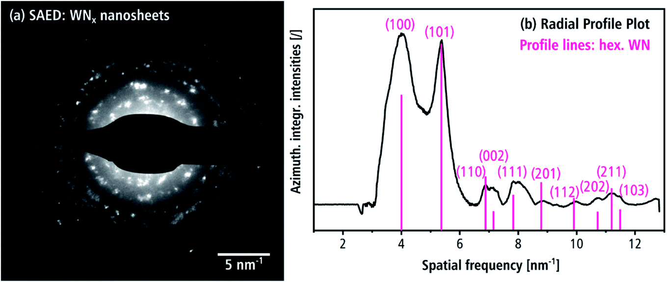 | ||
| Fig. 8 (a) SAED pattern of agglomerated WNx nanosheets with beam stop blocking the zero-order beam and (b) the corresponding azimuthally integrated intensity plot with Bragg reflections for δ-WN with hexagonal structure. The pink lines indicate the calculated positions and kinematic intensities of the Bragg reflections for the δ-WNx structure. | ||
| δ1-W2N3 | (006) at 3.9 nm−1 | (100), (101) at 4.0 nm−1 | (102) at 4.2 nm−1 |
| δ2-WN2 | (006) at 3.7 nm−1 | (101), (0−11), (−111) at 4.0 nm−1 | (012), (−102), (1−12) at 4.2 nm−1 |
Such nitrogen-rich crystal structures are indeed likely given the nitrogen-rich chemical compositions determined by EDXS as will be shown in the section “chemical composition”. Pink lines in Fig. 8(b) indicate the calculated kinematical intensities of the Bragg reflections. Deviations between calculated kinematical and experimental reflection intensities can be attributed to dynamical diffraction and texture effects, which often occur for plate-like morphologies.
With regard to a possible mix-up with tungsten carbides, there is one Pm2 isostructure with similar lattice parameters a1,2 = 2.90 Å and c = 2.85 Å.46 More information on the crystallinity of the carbon contamination will be obtained by analyzing the ELNES of the C–K edge in an EELS spectrum presented in the section on chemical composition.
Further investigations of the aforementioned texture of nanosheets were performed by analyzing moiré patterns of stacked nanosheets, which are frequently observed in TEM images taken at higher magnifications. The honeycomb pattern in Fig. 9(a) is particularly common. In this figure, a 15 nm-wide region is visible with a hexagonal tile pattern with one tile marked with a pink frame. In the FT image of the central region (cf. Fig. 9(b)), double reflections of the hexagonal WNx crystal structure in the [001] zone axis are observed. This is caused by the overlap of two WNx nanosheets, whose (001) basal planes are parallel but rotated around the c-axis by 5.8°. This rotation leads to a honeycomb pattern as shown by the simulation of two rotated planes with hexagonal structure in Fig. 9(c). In addition to the honeycomb moiré patterns, other patterns appear in TEM and HRTEM images. Fig. 9(d) shows an HRTEM image taken at the edge of a nanosheet aggregate as an example of a complex pattern. Most of the image shows stacked nanosheets. At the bottom, the amorphous C-support film is visible. The right stack of sheets is located to the right of the pink border line. Left and marked with a yellow line, is a single nanosheet, which partially overlaps the right nanosheet stack. Also shown are FT images of the pink-marked area in Fig. 9(g), the left nanosheet in Fig. 9(e), and the overlap region in Fig. 9(f). The right stack of nanosheets has a line-like moiré pattern with a periodicity of approximately 3 nm. Furthermore, there are hints of a superimposed hexagonal tile-like moiré pattern as indicated by the white lines in Fig. 9(d). According to the FT in Fig. 9(g), this complex pattern is created by three sheets rotated by 6 and 4.8° around the [001] zone axis. The left sheet (marked with a yellow line) does not contain a moiré pattern as shown by the FT in Fig. 9(e). However, the FT pattern in the overlap region between the pink and yellow lines in Fig. 9(f) is composed of the overlapping of the reflections in Fig. 9(e and g). It is remarkable that analyses of several stacked nanosheets yield exclusively rotation angles between 4° and 6°.
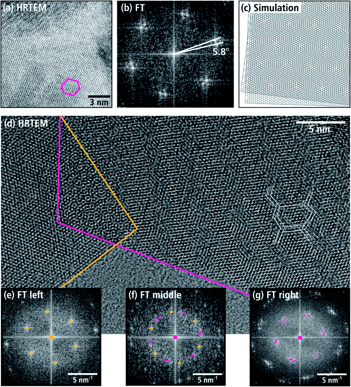 | ||
| Fig. 9 (a) TEM image of stacked WNx nanosheets, which show a honeycomb moiré pattern. (b) FT image of the moiré pattern area in (a). The pattern in (a) was simulated in (c) with a simple graphics program. (d) HRTEM image of an edge region of several stacked sheets with a complex moiré pattern (red) and a single sheet below (yellow). (e and g) FT images of the red and yellow marked area in (d), and (f) FT image of the overlap region. | ||
Defects with a striped contrast can be seen in several TEM images of larger nanosheet agglomerates such as in Fig. 10(a). The region in the yellow frame in (a) is shown with higher magnification in Fig. 10(b) with an FT of the largely disturbed region in the pink rectangle presented in Fig. 10(c). The FT can be indexed with the δ-WNx phase in [100] zone axis. The streaks along the [001] direction indicate the presence of two-dimensional defects on the (001) planes. Although a detailed analysis of the defect structure is not possible in Fig. 10(b), the FT analysis suggests the presence of stacking faults, where the stacking order…ABABAB… of the (001) planes in the hexagonal crystal structure is disturbed. Regions with high stacking fault densities are also observed in other regions of the nanosheet agglomerate.
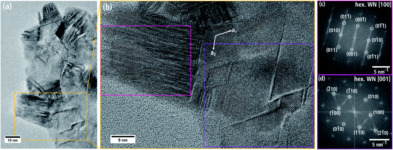 | ||
| Fig. 10 (a) HRTEM image of a WNx nanosheet agglomerate. (b) Magnification of the region marked in (a) by a yellow rectangle. The region marked with a pink frame in (b) shows a striped contrast induced by planar defects (most likely stacking faults) as further illustrated in (c) in the corresponding FT image. The region marked with a purple frame in (b) contains defects along the a1 and a2 directions of the hexagonal structure, which induce streaks in the respective FT image (d). | ||
Another type of defect structure can be seen in Fig. 10(b) on the right-hand side. V-shaped defects cross the (001) layer with typical hexagonal angles of 60° and 120°. The defect directions are parallel to the hexagonal a1 and a2 axes marked by arrows in Fig. 10(b). Close inspection of regions in the vicinity of these defects reveals a change of fringe contrast with respect to the orientation and, partly, the fringe distance. These regions are very thin and span merely a few atomic planes. They induce streaks in the FT image in Fig. 10(d), which extend between the (![[2 with combining macron]](https://www.rsc.org/images/entities/char_0032_0304.gif) 10), (
10), (![[1 with combining macron]](https://www.rsc.org/images/entities/char_0031_0304.gif) 10), (00) and the respective reflections (20), (10), (100). Due to the change of orientation and distance of the fringes the defects resemble nanotwins.
10), (00) and the respective reflections (20), (10), (100). Due to the change of orientation and distance of the fringes the defects resemble nanotwins.
3.2 Chemical composition
The chemical composition of the WNx aggregates was analyzed with EDXS. Fig. 11(a) shows a HAADF-STEM image of a representative nanocrystalline agglomerate (batch a) with the corresponding element distribution images of W (red), N (yellow) and O (blue). The intensity of the colors in the elemental maps is a qualitative measure of the amount of the corresponding element, which depends also on the local thickness of the aggregate. The local intensities of W and N distribution resemble the intensity of the HAADF-STEM image as expected but a considerable amount of O is also detected. The aggregate lies on the edge of the carbon support film, which is not visible in the HAADF-STEM image due to its low scattering power. The carbon film surrounding the aggregate contains a background concentration of N (yellow) and O (blue). In contrast, W is only detected in the area of the aggregate. Quantified regions on the aggregate and in the surroundings are marked in the W map with the results shown in Table 3. The stoichiometry measured over an area of approximately 20 nm at point 1 is WN0.7. Furthermore, a high O concentration of 23 at% is found in the aggregate and 15 at% in the carbon background film. Another contaminant is Si with 3 at% in the aggregate and 7 at% on the carbon support.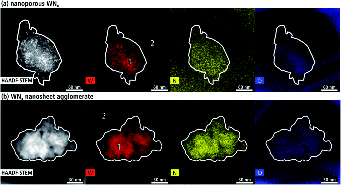 | ||
| Fig. 11 Element distributions obtained by EDXS mappings showing the W (red), N (yellow), and O (blue) distributions with corresponding HAADF-STEM image of a (a) representative nanoporous aggregate and (b) agglomerated WNx nanosheet. | ||
| EDXS quantification area | Elements [at%] | ||||
|---|---|---|---|---|---|
| C | N | O | W | Si | |
| Nanocrystalline WNx aggregate | 52 | 4 | 23 | 6 | 3 |
| Carbon support film | 74 | — | 15 | — | 7 |
| Agglomerated WNx nanosheets | 67 | 11 | 16 | 3 | — |
| Background | 78 | 1 | 16 | — | 3 |
The chemical composition of a representative WNx nanosheet agglomerate is displayed in Fig. 11(b). The intensity of the agglomerate in the HAADF-STEM image resembles the intensities of the W (red) and N (yellow) distribution while the distribution of O over the region of the agglomerate shows a rather homogeneous intensity. O is also detected in a circular region around the agglomerate. The composition was quantified in regions marked with numbers in the W map. A homogeneous region of about 30 nm and 60 nm in diameter was selected for quantification in point 1 and 2, respectively. The stoichiometry of the nanosheet agglomerate is WN3.7 (cf. Table 3), which is a nitrogen surplus for common tungsten nitride crystal structures. Quantifications of other nanosheet agglomerates yield compositions with WN1.7–3.7. These nitrogen-rich compositions are in agreement with δ1-W2N3, δ2-W2N3 and δ2-WN2, which are structural derivatives of the hexagonal WN structure revealed by Fig. 8.7,11 High levels of N above WN2 are attributed to the high amount of amines in the synthesis, which remain as residuals within and on top of the WNx nanosheets as indicated by the SE-SEM in Fig. 4(b). Similar O concentrations of 16 at% are contained in the support film (measuring point 2) and the agglomerate (measuring point 1).
The presence of O and Si can be assigned to SiO2 glassware used during synthesis. The circular-shaped O contamination could be connected with growing contamination during electron-microscopy analysis. The lack of crystalline WOx phases is supported by the fact that electron diffraction and HRTEM studies did not yield indications for crystal structures expected for WOx.
High C concentrations arise from the carbon support film, contamination in the microscope and solvent/surfactant residues. Other trace contaminants not listed in Table 3 are F, Cl, Cu and Fe. Cl is contained in the WCl6 precursor. Multiple sample areas, such as the agglomerate in Fig. 11(b) show high F concentrations due to corrosion of the polytetrafluoroethylene magnetic stir bar. Cu is due to the Cu grid of the TEM samples. Fe results from stray X-rays of the objective-lens pole piece.
The ELNES of the C–K edge in EELS spectra yields information on the crystallinity of the carbon detected by EDXS. It is important to distinguish the formation of crystalline WC from the amorphous C-support film, contamination in the microscope and synthesis residues, which are expected to be present in amorphous form. Fig. 12 shows an EELS spectrum acquired in the region of a nanocrystalline WNx aggregate, which shows the C–K edge with an onset of 285 eV and the N–K edge with an onset of 400 eV. The ELNES of the C–K edge is almost structure-less and demonstrates that carbon is present in disordered form as expected from the amorphous carbon support film, contamination in the microscope and synthesis residues.47 This is in strong contrast with the ELNES of the C–K edge of crystalline carbides as shown for, e.g. TiC, with several pronounced peaks,48 which are not present in the spectrum in Fig. 12. The intensity of the N–K edge shows a low intensity, which is, however, in accordance with the EDXS results where the C content strongly exceeds the N concentration (cf. Table 3).
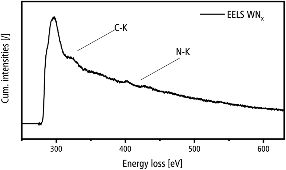 | ||
| Fig. 12 EELS spectrum of a nanocrystalline WNx aggregate in the energy loss range of the C–K and N–K edges. | ||
4. Discussion
Nanoscale WNx materials were produced with a soft template synthesis and evaporation-induced self-assembly. Depending on the concentration of long-chained amines during synthesis, WNx with different crystal structures and morphologies was obtained. This resulted in a material consisting of nanocrystalline WNx aggregates and, by increasing the long-chain amines in the synthesis, a material consisting of WNx nanosheets. Synthesis, preparation, and analysis had to be conducted under inert gas and with the use of a TEM transfer holder as exposure to any water or oxygen would result in swift material deterioration. The nanocrystalline WNx aggregates predominantly consist of 1.6 to 3.2 nm small crystallites, which form a porous substructure. According to FT, SAED analysis and EDXS, the crystallites occur in the cubic β-phase with a composition of WN0.7 consistent with the cubic phase with N concentrations between WN0.6–1.0.6–8The second WNx nanomaterial consists of nanosheets with lateral dimensions up to several 500 nm and thicknesses between 0.7 and 4.9 nm. The nanosheets can be stacked, with frequent rotations of 4–6° around the c-axis of the hexagonal crystal structure. In contrast to the small crystallites of the nanocrystalline material with cubic structure, the nanosheets crystallize in the δ-phase family comprising various hexagonal crystal structures (cf. Table 1) and partly nitrogen-rich compositions. The change in the crystal structure and material morphology of nanocrystalline aggregates with small (isometric) crystallites to nanosheets is attributed to the higher proportion of amines in the synthesis of the nanosheet material, which leads to a higher N concentration of WNx. With such nitrogen-rich nitrides, a dominance of the hexagonal phase is expected, because only the hexagonal structure is stable for N concentrations above 50 at%.6,9 High N concentrations above up to WN3.7 are obtained in EDXS quantifications. However, it is not completely clear how much of the nitrogen can be assigned to the crystal phase and how much to amine residues, which can be present as indicated by SE-SEM images (cf. Fig. 5).
Nanosheets frequently contain regions with high stacking-fault densities and show signs of nanotwins (cf. Fig. 10). A high density of stacking faults can occur in materials with a hexagonal crystal structure that are exposed to mechanical stress at low temperatures.49 The predominance of stacking faults over dislocations is expected for such hexagonal crystal structures since only few suitable slip systems are available for dislocation glide in contrast to cubic crystal structures.50 One possible cause for the deformation of the nanosheets could be bending of the layers. Another source of deformation can result from the preparation of the hardened powder after synthesis and ultrasound treatment to disperse the material. Nanotwins are another type of defect observed in Fig. 10(b). Nanotwinning has been observed in several material groups and is thought to be a deformation mechanism at moderate stresses and lower temperatures.49,51
On the other hand, the high stacking fault density in Fig. 10(b) in the pink frame could also be interpreted as a transformation structure between cubic and hexagonal crystal structures. Cubic and hexagonal structures differ in the stacking order of the dense-packed cubic (111) planes (…ABCABC…) and hexagonal (001) planes (…ABABAB…). Transformation between the two structures is possible by introducing stacking faults, which has already been frequently observed, e.g. in ref. 52–54. This interpretation is further supported by the observed cubic crystal structure in the nanocrystalline WNx material, which indicates that WNx nanomaterials of batch a and b are close to the phase boundary, which is governed by their N concentration.6
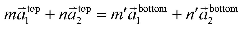
Nanosheets show another structural peculiarity. Rotations of nanosheets around the hexagonal c-axis are frequently observed within a limited angular range between 4° and 6°. A possible explanation for the preference of such small rotation angles can be found if the conditions for the formation of commensurate structures are considered. The atom arrangement at the interface between two nanosheets can be described by eqn (1)
 | (1) |
 and
and 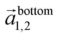 in the hexagonal (001) plane of the top and bottom nanosheet, which are rotated against each other by an angle θ.55 Commensurate superlattices require that m, m′, n and n′ are integer numbers. For specific θ, a periodic two-dimensional (i.e. a commensurate) superlattice is formed at the interface between the nanosheets. Commensurate superstructures are easily recognized by moiré patterns in (HR)TEM images (cf. Fig. 9(a and c)) because they show two-dimensional translational symmetry. Incommensurate structures, on the other hand, lack translational symmetry and do not show a long-range periodicity. It was already demonstrated that a large number of commensurate structures exists for (001) planes in hexagonal structures at small rotation angles up to about 7° and angles between 53° and 60°, which are equivalent to small rotation angles for symmetry reasons.55 In contrast, only few commensurate superstructures exist for rotation angles between 7° and 53°. Most structures in this interval of rotation angles do not show a long-range translational symmetry. Since incommensurate structures are difficult to stabilize, the formation of commensurate structures with small rotation angles will be strongly preferred, which explains the dominance of small rotation angles.56,57 At first sight, this explanation seems to be in contradiction with the fact that we do not observe rotation angles below 4°. However, this can be understood by considering the periodicity of the superstructure dSL, which is given for small rotation angles θ by eqn (2)
 | (2) |
Only an educated guess is possible on the reasons why nanosheets are rotated against each other. In general, any kind of strain during synthesis and further processing could lead to rotations between nanosheets. Disarrangement during synthesis could be another possible reason for the generation of sheets that are rotated against each other. For example, evaporation of the solvent between the nanosheets could cause such a disordered stacking if the evaporation of the solvent is too fast, leading to a more inhomogeneous arrangement of the in solution floating nanosheets to form the observed stacks of nanosheets. An evaporation-induced disorder of stacked crystals with internal sheet-like morphology has previously been observed in swellable clay minerals, notably smectites, where water can enter and exit the interlayer space between the sheets. To test this explanation model, multiple syntheses with differing evaporation conditions would have to be performed, which was not part of this work.
5. Conclusions
It was demonstrated in this work that the morphology and phase of WNx nanomaterials can be controlled by a new alkylamide-assisted synthesis. Depending on the concentration of long-chain amine surfactants, nanocrystalline WNx aggregates with a nm-scaled crystallinity and WNX nanosheets are produced. With increasing amine concentration, the N content in the synthesized material is increased and leads to a phase transition from the cubic WNx phase with concentrations up to 50 at% N to the hexagonal phase with higher N concentrations. This process is accompanied by a morphology change from nanocrystalline aggregates to nanosheets. The controlled synthesis of a material with two-dimensional morphology is particularly interesting with respect to other intensely studied two-dimensional materials like graphene and chalcogenides.The nanocrystalline aggregates contain 0.8 to 7.6 nm small cubic β-WNx crystallites with a composition of WN0.7, which is compatible with the stability range of the β-phase. WNX nanosheets, on the other hand, consist of δ-WNx with hexagonal structure or variants of this phase with higher N concentrations of WN1.7–3.7. Nanosheets are characterized by lateral widths of up to 500 nm and sheet thicknesses between 0.7 and 4.9 nm. Regions with high stacking-fault densities are indicative of a cubic-to-hexagonal phase transformation. Nanosheets are frequently stacked with rotations of 4–6° around the c-axis of the hexagonal crystal structure. This limited rotation-angle range can be understood by the large number of commensurate structures at nanosheet interfaces at small rotation angles while commensurate structures for large rotation angles are rare.
The results of the two WNx nanomaterials are particularly of interest for other syntheses of WNx nanomaterials. Beyond WNx, the material properties produced with this method are of significance for related nanoscaled transition metal nitrides due to the chemical and structural similarities in this material group.59,60 As shown by Rein, nanoporous CrNx, MoNx and TaNx can be produced by similar lyotropic phases using the respective transition metal nitride salts.61 Therefore, nanosheets of a variety of transition metal nitrides should be possible too, which could eventually lead to a completely new class of 2D materials. Furthermore, the observed structural changes that the aggregates undergo with increasing surfactant concentration provide insight into the self-assembly dynamics of alkylamines. However, more fundamental research is needed. Particularly the special structural properties of the WNx nanosheets trigger further fundamental questions about crystal growth, stacking and the exact role of surfactants in these processes.
Conflicts of interest
There are no conflicts to declare.Acknowledgements
The authors thank the Deutsche Forschungsgemeinschaft (DFG) for funding (FE911/10-1, GE 841/28). MH acknowledges funding by the Deutsche Forschungsgemeinschaft (DFG, German Research Foundation) under Germany's Excellence Strategy – 2082/1 – 390761711 and thanks the Carl Zeiss Foundation for financial support.References
- S. Das, J. A. Robinson, M. Dubey, H. Terrones and M. Terrones, Annu. Rev. Mater. Res., 2015, 45, 1–27 CrossRef CAS.
- S. Z. Butler, S. M. Hollen, L. Cao, Y. Cui, J. A. Gupta, H. R. Gutiérrez, T. F. Heinz, S. S. Hong, J. Huang, A. F. Ismach, E. Johnston-Halperin, M. Kuno, V. V. Plashnitsa, R. D. Robinson, R. S. Ruoff, S. Salahuddin, J. Shan, L. Shi, M. G. Spencer, M. Terrones, W. Windl and J. E. Goldberger, ACS Nano, 2013, 7, 2898–2926 CrossRef CAS PubMed.
- W. Huang, L. Gan, H. Li, Y. Ma and T. Zhai, CrystEngComm, 2016, 18, 3968–3984 RSC.
- D. Golberg, Y. Bando, Y. Huang, T. Terao, M. Mitome, C. Tang and C. Zhi, ACS Nano, 2010, 4, 2979–2993 CrossRef CAS PubMed.
- J. H. Warner, M. H. Rümmeli, A. Bachmatiuk and B. Büchner, ACS Nano, 2010, 4, 1299–1304 CrossRef CAS PubMed.
- H. A. Wriedt, Bull. Alloy Phase Diagrams, 1989, 10, 358–367 CrossRef CAS.
- S. Wang, X. Yu, Z. Lin, R. Zhang, D. He, J. Qin, J. Zhu, J. Han, L. Wang, H. K. Mao, J. Zhang and Y. Zhao, Chem. Mater., 2012, 24, 3023–3028 CrossRef CAS.
- V. I. Khitrova, Crystallogr. Rep., 1959, 4, 513–520 Search PubMed.
- N. Schönberg, Acta Metall., 1954, 2, 427–432 CrossRef.
- V. I. Khitrova and Z. G. Pinsker, Crystallogr. Rep., 1958, 3, 545–553 CAS.
- V. I. Khitrova, Crystallogr. Rep., 1962, 6, 439–442 Search PubMed.
- J. S. Becker and R. G. Gordon, Appl. Phys. Lett., 2003, 82, 2239–2241 CrossRef CAS.
- J. H. Kim and K. L. Kim, Appl. Catal., A, 1999, 181, 103–111 CrossRef CAS.
- M. Takeyama and A. Noya, Jpn. J. Appl. Phys., Part 1, 1997, 36, 2261–2266 CrossRef CAS.
- Y. Dong and J. Li, Chem. Commun., 2015, 51, 572–575 RSC.
- Y. T. Kim, C. W. Lee, C. S. Kwon, S. K. Min and S. K. Park, in 1994 International Electron Devices and Materials Symposium, EDMS 1994, IEEE, 1994, pp. 8–6-21–8-6-24 Search PubMed.
- Y. M. Sun, E. R. Engbrecht, T. Bolom, C. Cilino, J. H. Sim, J. M. White, J. G. Ekerdt and K. Pfeifer, Thin Solid Films, 2004, 458, 251–256 CrossRef CAS.
- S. T. Oyama, Catal. Today, 1992, 15, 179–200 CrossRef CAS.
- J. S. J. Hargreaves, Coord. Chem. Rev., 2013, 257, 2015–2031 CrossRef CAS.
- C. Giordano and M. Antonietti, Nano Today, 2011, 6, 366–380 CrossRef CAS.
- R. B. Levy and M. Boudart, Science, 1973, 181, 547–549 CrossRef CAS PubMed.
- Q. Liang, G. Brocks, X. Zhang and A. Bieberle-Hütter, J. Phys. Chem. C, 2019, 123, 26289–26298 CrossRef CAS.
- J. Xie and Y. Xie, Chem.–Eur. J., 2016, 22, 3588–3598 CrossRef CAS PubMed.
- X. Zou and Y. Zhang, Chem. Soc. Rev., 2015, 44, 5148–5180 RSC.
- S. Dong, X. Chen, X. Zhang and G. Cui, Coord. Chem. Rev., 2013, 257, 1946–1956 CrossRef CAS.
- H. Jin, H. Zhang, J. Chen, S. Mao, Z. Jiang and Y. Wang, J. Mater. Chem. A, 2018, 6, 10967–10975 RSC.
- J. Diao, Y. Qiu, S. Liu, W. Wang, K. Chen, H. Li, W. Yuan, Y. Qu and X. Guo, Adv. Mater., 2020, 32, 1905679 CrossRef CAS PubMed.
- H. Liu, Z. S. Wu, L. Huang, B. W. Zhang, L. C. Yin, C. Y. Xu and L. Zhen, J. Mater. Chem. A, 2021, 9, 11323–11330 RSC.
- K. A. Papadopoulou, A. Chroneos, D. Parfitt and S. R. G. Christopoulos, J. Appl. Phys., 2020, 128, 170902 CrossRef CAS.
- A. Bhat, S. Anwer, K. S. Bhat, M. I. H. Mohideen, K. Liao and A. Qurashi, npj 2D Mater. Appl., 2021, 5, 1–21 CrossRef.
- O. Eksik, J. Gao, S. A. Shojaee, A. Thomas, P. Chow, S. F. Bartolucci, D. A. Lucca and N. Koratkar, ACS Nano, 2014, 8, 5282–5289 CrossRef CAS PubMed.
- J. S. Son, X. D. Wen, J. Joo, J. Chae, S. Baek, K. Park, J. H. Kim, K. An, J. H. Yu, S. G. Kwon, S. H. Choi, Z. Wang, Y. W. Kim, Y. Kuk, R. Hoffmann and T. Hyeon, Angew. Chem., Int. Ed., 2009, 48, 6861–6864 CrossRef CAS PubMed.
- C. Huang, X. Qian and R. Yang, Mater. Sci. Eng., R, 2018, 132, 1–22 CrossRef.
- D. H. Gregory, Coord. Chem. Rev., 2001, 215, 301–345 CrossRef CAS.
- D. R. Glasson and S. A. A. Jayaweera, J. Appl. Chem., 2007, 18, 77–83 CrossRef.
- I. P. Parkin and A. M. Nartowski, Polyhedron, 1998, 17, 2617–2622 CrossRef CAS.
- H. Wang, E. J. Sandoz-Rosado, S. H. Tsang, J. Lin, M. Zhu, G. Mallick, Z. Liu and E. H. T. Teo, Adv. Funct. Mater., 2019, 29, 1902663 CrossRef.
- H. Yu, X. Yang, X. Xiao, M. Chen, Q. Zhang, L. Huang, J. Wu, T. Li, S. Chen, L. Song, L. Gu, B. Y. Xia, G. Feng, J. Li and J. Zhou, Adv. Mater., 2018, 30, 1805655 CrossRef PubMed.
- H. Jin, L. Li, X. Liu, C. Tang, W. Xu, S. Chen, L. Song, Y. Zheng and S. Z. Qiao, Adv. Mater., 2019, 31, 1902709 CrossRef PubMed.
- O. Wenzel, V. Rein, R. Popescu, C. Feldmann and D. Gerthsen, Microsc. Microanal., 2019, 26, 102–111 CrossRef PubMed.
- V. Rein, O. Wenzel, R. Popescu, D. Gerthsen and C. Feldmann, J. Mater. Chem. C, 2018, 6, 4450–4456 RSC.
- C. A. Schneider, W. S. Rasband and K. W. Eliceiri, Nat. Methods, 2012, 9, 671–675 CrossRef CAS PubMed.
- P. A. Stadelmann, Ultramicroscopy, 1987, 21, 131–145 CrossRef CAS.
- P. F. Schmidt, Praxis der Rasterelektronenmikroskopie und Mikrobereichsanalyse, Expert-Verlag GmbH, 1994 Search PubMed.
- Z. Abdullaeva, E. Omurzak, C. Iwamoto, H. Okudera, M. Koinuma, S. Takebe, S. Sulaimankulova and T. Mashimo, RSC Adv., 2013, 3, 513–519 RSC.
- K. Page, J. Li, R. Savinelli, H. N. Szumila, J. Zhang, J. K. Stalick, T. Proffen, S. L. Scott and R. Seshadri, Solid State Sci., 2008, 10, 1499–1510 CrossRef CAS.
- D. Shindo, T. Musashi, Y. Ikematsu, Y. Murakami, N. Nakamura and H. Chiba, J. Electron Microsc., 2005, 54, 11–17 CrossRef CAS PubMed.
- F. Hofer, P. Warbichler, P. B. Anderson and R. Pitonak, Mikrochim. Acta, 1990, 101, 243–249 CrossRef.
- D. Barba, E. Alabort, S. Pedrazzini, D. M. Collins, A. J. Wilkinson, P. A. J. Bagot, M. P. Moody, C. Atkinson, A. Jérusalem and R. C. Reed, Acta Mater., 2017, 135, 314–329 CrossRef CAS.
- W. F. Hosford, Mechanical behavior of materials, Cambridge University Press, Cambridge, 2005 Search PubMed.
- L. Kovarik, R. R. Unocic, J. Li, P. Sarosi, C. Shen, Y. Wang and M. J. Mills, Prog. Mater. Sci., 2009, 54, 839–873 CrossRef CAS.
- R. Sarkar, P. Ghosal, K. S. Prasad, T. K. Nandy and K. K. Ray, Philos. Mag. Lett., 2014, 94, 311–318 CrossRef CAS.
- Y. Koizumi, S. Suzuki, K. Yamanaka, B. S. Lee, K. Sato, Y. Li, S. Kurosu, H. Matsumoto and A. Chiba, Acta Mater., 2013, 61, 1648–1661 CrossRef CAS.
- Z. He, J. L. Maurice, Q. Li and D. Pribat, Nanoscale, 2019, 11, 4846–4853 RSC.
- W. Yao, E. Wang, C. Bao, Y. Zhang, K. Zhang, K. Bao, C. K. Chan, C. Chen, J. Avila, M. C. Asensio, J. Zhu and S. Zhou, Proc. Natl. Acad. Sci. U. S. A., 2018, 115, 6928–6933 CrossRef CAS PubMed.
- C. R. Woods, L. Britnell, A. Eckmann, R. S. Ma, J. C. Lu, H. M. Guo, X. Lin, G. L. Yu, Y. Cao, R. V. Gorbachev, A. V. Kretinin, J. Park, L. A. Ponomarenko, M. I. Katsnelson, Y. N. Gornostyrev, K. Watanabe, T. Taniguchi, C. Casiraghi, H. J. Gao, A. K. Geim and K. S. Novoselov, Nat. Phys., 2014, 10, 451–456 Search PubMed.
- C. R. Woods, F. Withers, M. J. Zhu, Y. Cao, G. Yu, A. Kozikov, M. Ben Shalom, S. V. Morozov, M. M. Van Wijk, A. Fasolino, M. I. Katsnelson, K. Watanabe, T. Taniguchi, A. K. Geim, A. Mishchenko and K. S. Novoselov, Nat. Commun., 2016, 7, 10800 Search PubMed.
- P. Moon and M. Koshino, Phys. Rev. B: Condens. Matter Mater. Phys., 2012, 85, 195458 CrossRef.
- D. H. Gregory, J. Chem. Soc., Dalton Trans., 1999, 259–270 RSC.
- W. Lengauer, in Encyclopedia of Inorganic and Bioinorganic Chemistry, John Wiley & Sons, Ltd, Chichester, UK, 2015, pp. 1–24 Search PubMed.
- V. Rein, Verwendung mizellarer Systeme zur Synthese von Metallphosphat-Nano containern und nanoporösen Metallnitriden, Cuvillier Verlag, Göttingen, 2019 Search PubMed.
| This journal is © The Royal Society of Chemistry 2021 |