DOI:
10.1039/D1RA04166E
(Paper)
RSC Adv., 2021,
11, 26655-26665
Biophotonic sensor design using a 1D defective annular photonic crystal for the detection of creatinine concentration in blood serum
Received
29th May 2021
, Accepted 6th July 2021
First published on 4th August 2021
Abstract
A new biophotonic sensor composed of a porous silicon (PSi)-based one-dimensional (1D) defective annular photonic crystal (APC) was designed and theoretically investigated using a modified transfer matrix method (TMM) in terms of cylindrical coordinates. The proposed biosensor was found to be capable of sensing very minute variations in the refractive index of blood serum samples of different creatinine concentrations. It can be considered as a useful tool for diagnosing mild to chronic kidney diseases by measuring the creatinine concentration in the blood serum samples of patients. The biosensor design [(AB)N/2D(AB)N/2/Si] is composed of two 1D APCs (AB)N/2 associated with a defect layer D of a blood serum sample of thickness dd whose creatinine concentration is to be determined. Both 1D APCs are made up of two alternate PSi layers A and B with porosity ratios of 34% and 87%, respectively. Moreover, our proposed biophotonic sensor demonstrated a high value of sensitivity (S) between 637.73 and 640.29 nm per RIU, a quality factor (Q) between 1.51 × 10⁵ and 0.74 × 10⁵, and a figure of merit (FOM) between 2.6 × 10⁴ and 1.96 × 10⁴ RIU, corresponding to a blood serum sample whose creatinine concentration varied between 80.90 to 85.28 μmol L−1. The limit of detection (LOD) was of the order of 10−6 RIU. This low value LOD confirmed that our biosensor is capable of noticing any minute change in the wavelength up to an order of 10−6. Compared with previous works, the proposed biosensor design can be easily realized and offers high performance at normal incidence, which allows overcoming the complications involved while achieving a high value of sensitivity in planar PC-based biosensor designs at oblique incidence. Beside this, there is also a possibility to explore this work further for the development of various APC-based biosensing designs with the aim to study various human body fluids.
1. Introduction
Photonic crystals (PCs) are periodic structures and have attracted widespread attention due to their potential and useful applications in modern photonic technology, which is a fast developing field of research.1–7 The concept of PCs was introduced by the pioneering work of photonic bandgaps (PBGs) by Yablonovitch and photon localization by John.8,9 PCs are composed of composite multilayer structures, in which the modulation of refractive index occurs in spatial directions, such as one-dimensional (1D), two-dimensional (2D), and three dimensional (3D) directions in space. One of the promising characteristics of PCs is the control of the propagation of the electromagnetic waves of different frequencies due to the existence of PBG, which is an optical analogy of the electronic bandgap (EBG) in solids.10,11 The PBG consists of frequency regions in which the propagation of electromagnetic waves (EMWs) is not allowed due to Bragg scattering. The frequencies of incident EMWs outside are not attenuated and are allowed to pass through the structure. The breaking of the periodicity by inserting a defect layer inside PC generates a defect mode inside PBG due to the confinement of EMWs through the defect layer molecules.12–14 The position of these defect modes can be further modulated inside PBG depending on the refractive index and thickness of the defect layer region. This remarkable property of tuning the defect mode inside the PBG of defective PCs has inspired various research groups worldwide in their attempts to develop high-performance biosensors.15–20 These biosensors are remarkably attractive to the biomedical and biochemical fields due to their tremendous sensing and detecting capabilities.21–24 PC-based biosensors have been widely designed and fabricated for the detection of temperature, hydrostatic pressure, acoustic waves, and magnetic fields.25,26
In addition to conventional planar 1D PCs, annular photonic crystals (APCs) have attracted much attention in recent years due to the outstanding results from theoretical findings and the improved fabrication techniques.27–30 Basically, an early study by Kaliteevski et al. attracted the attention of various research groups toward APCs after they studied the propagation of electromagnetic waves inside APCs with the help of a modified transfer matrix method for cylindrical multilayer structures.31 Many researchers have since carried out innovative work showing better sensing capabilities for APC structures in comparison to planar photonic structures.32–34 Moreover high-performance APC-based sensor designs using different materials are easy to realize and have promising applications in the field of laser emission, optical communication, and optoelectronics.35–37 For example Mehaney et al. proposed a high-performance biophotonic design capable of sensing chemical and biomedical fluids that was composed of 1D ternary APCs, which worked at the Tamm/Fano resonance state and exhibited a sensitivity (S) of 6770 nm per RIU with a quality (Q) factor of 662.38 A high-performance temperature sensor design using 1D defective APCs with a sensitivity of 11 nm per 1000 °C and a figure of merit (FOM) of 0.218 per °C was proposed by Abdulla et al.39 The aforesaid piece of excellent research work opened a new gateway for designing 1D APC-based biosensors capable of detecting minute changes in the chemical or biological properties of a sample by producing a readable signal to diagnose various diseases in the human body efficiently and rapidly in comparison to the available conventional methods, which tend to be time consuming and highly expensive.
A biosensor is a compact device capable of detecting changes in biological or chemical systems by producing a signal proportional to the concentration of the analyte to be examined.40,41 A typical biosensor consists of five parts: (1) the substance in the liquid form, called the analyte, which needs to be examined; (2) the bioreceptor to characterize the analyte; (3) the transducer, which produces a measurable optical, electrochemical, magnetic or electrical signal, depending on the bioreceptor interaction; (4) the electronic circuit, which processes and prepares the transduced signal for display; and (5) arguably the most important part of any biosensor, which is the combination of the hardware and software that allows displaying the results in a user-friendly manner.42–45
In the past few decades, porous materials have attracted much attention due to their potential in a wide range of fields, from opto-to-microelectronics, optics, biomedicine, and fluid and gas sensing applications, etc.46–48 Porous silicon (PSi) is one such material, in which nanometric tiny pores are embedded on the silicon wafer by an electrochemical etching technique under the influence of an electric current in a hydrofluoric acid electrolyte.49 Due to its considerable surface area and versatile surface chemistry, PSi reflects amazing optical, mechanical, and electronic properties, such as high optical sensitivity. The above-mentioned qualities make PSi a suitable candidate for designing both planar and annular PCs. Besides this, the fabrication of PSi with a modulating porosity can be easily achieved by variation of the electric current density during the electrochemical etching process, which allows a precise control over the properties of the PSi material layer.50 Moreover it is an economical, fast, and simple one-step process.
Nowadays, optical biosensors based on photonic crystal technology have been widely used in medical fields because of their accuracy, cost effectiveness, easy handling, and quick response.51–53 These biosensors are used as an important diagnostic tool for finding kidney-, sugar-, and heart-related diseases by examining the concentration of creatinine, glucose, and cholesterol, respectively, in the fluids of the human body. The metabolic processes in a biological system are responsible for producing waste products due to the normal breakdown of muscle cells, called creatinine. Hence the extraction of creatinine from biological systems is very important. This operation is done by healthy kidneys, which take creatinine out of the blood and put it into the urine to exit the body. When the kidneys are not working well, creatinine builds up in the blood, and so monitoring the creatinine level in the blood is a very important step for gaining preliminary knowledge of the kidney functioning. It also helps to identify kidney infections and diseases from a moderate to advanced level. The two most popular conventional methods for determination of the creatinine concentration in blood and urine are Jaffe's method and the enzymatic method.54 Both the Jaffe and enzymatic methods have been found to be able to meet the analytical performance requirements in routine use. However, the enzymatic method was found to have a better performance for low creatinine levels.
The present work aimed to extend the findings revealed by Aly et al. and to study the performance of a biophotonic sensor for the detection of the creatinine concentration in blood serum, based on a 1D defective planar photonic crystal of sensitivity of 306.25 nm per RIU at an oblique incidence of 85°.55 In PCs, it is very difficult to adjust the angle of incidence for obtaining the optimum results. Therefore, an attempt was made here to achieve better biosensing results at normal incidence in comparison to the aforementioned piece of excellent work of Aly and co-workers.55 In this work, we investigated theoretically a 1D defective APC structure for the detection of the creatinine concentration in blood, with a sensitivity between 637.73 and 640.29 nm per RIU at normal incidence depending on the concentration level of creatinine in the blood serum ranging between 80.9 and 85.28 μmol L−1.
The theoretical model and formulation of the proposed 1D defective APC-based biophotonic sensor capable of detecting the creatinine concentration in blood serum with the help of a modified transfer matrix method for cylindrical multilayer structures are detailed in Section 2. The Results and discussions pertaining to the work performed for studying the transmission characteristics of the proposed biophotonic sensor are given in Section 3. Finally, the Conclusions are mentioned in Section 4. To the best of our knowledge, this is first time 1D defective APC has been used for detecting the creatinine concentration in blood serum, with an average sensitivity of 638.91 nm per RIU, which could help to diagnose kidney dysfunction in patients.
2. Biosensor design and theoretical analysis
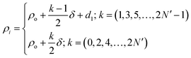
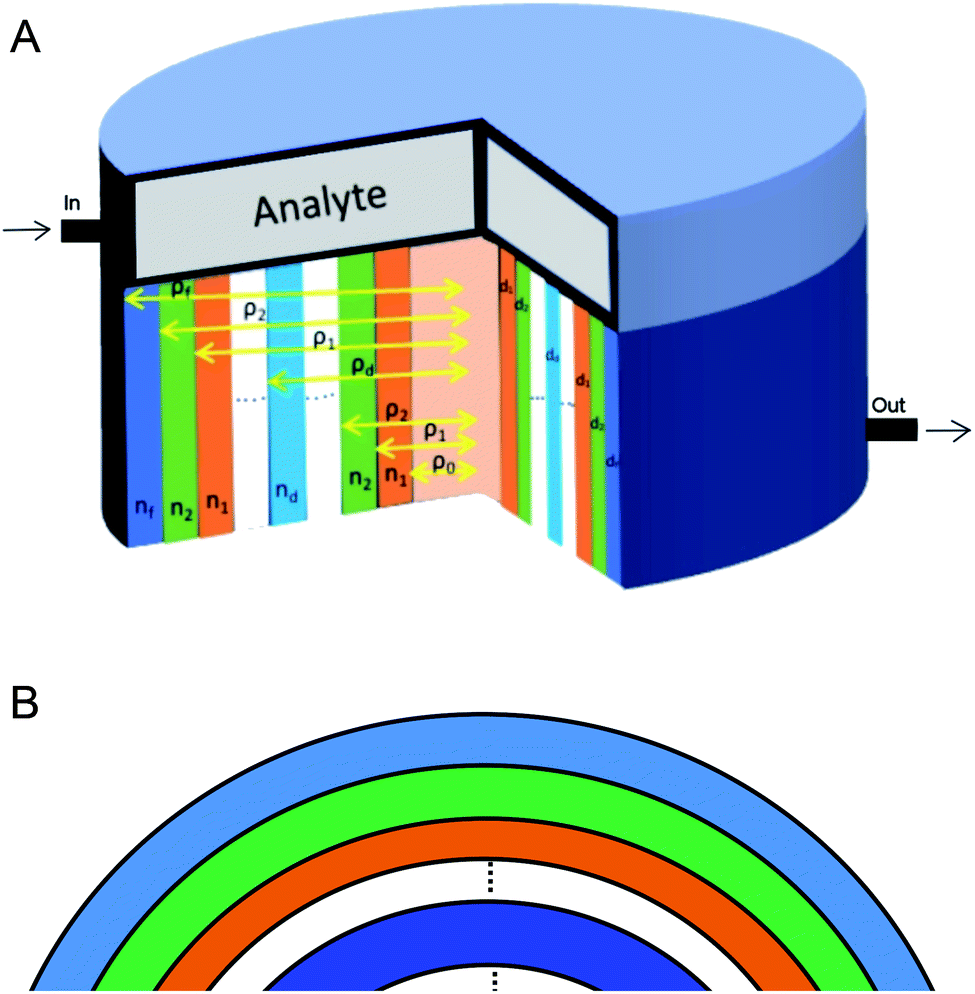
The proposed biosensor consisted of a 1D annular photonic crystal with defects. This design utilized periodic cylindrical coaxial multilayers, which allowed a core of radius ρ0. The refractive index of each cylindrical layer of this biosensor was modulated periodically as a function of the radial distance from the axis of symmetry, as shown in Fig. 1. In the proposed design [(AB)N/2D(AB)N/2], the two APCs, namely APC1 and APC2, were joined together through a cylindrical defect layer D of thickness dd and refractive index nd. The periods of both the APCs structures were N/2. The entire structure [(AB)N/2D(AB)N/2/substrate] was fabricated over a substrate of refractive index nf. Here A and B represent PSi coaxial cylindrical layers of porosity P1 and P2, respectively. The thickness and refractive index of PSi layers A and B were d1, d2 and n1, n2, respectively. The radial distance (ρi) between the axis of the symmetry of the structure and the outer edge of the concentric cylindrical layer i is given by:28–30| |
 | (1) |
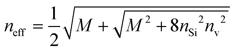
here, δ (=d1 + d2) and N′ (=N/2) are used to describe the period and period number of both APC1 and APC2. The magnetic permeability of the PSi layer was assumed to be 1 due to its non-magnetic behavior. APC1 and APC2 were both composed of two alternate PSi layers of different porosities. The effective refractive index of PSi layers is governed by Burgmann's effective medium approximation as:38,49,50| |
 | (2) |
here nv, nSi, and neff represent the refractive indices of the voids of the PSi layer, silicon wafer, and PSi layer, respectively. The effective refractive index (neff) of the PSi layer is dependent on the porosity ratio (P) and the refractive index of the analyte (nv) to be filled inside the hollow pores of both the PSi layers A and B. Eqn (2) can be rewritten to obtain an expression for the neff of the PSi layer in terms of nv, nSi, and P as:38,49| |
 | (3) |
here, M = 3P(nv2 − nSi2) + (2nSi2 − nv2).
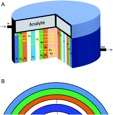 |
| | Fig. 1 (a) Schematic design of the 1D defective APC structure with an inner core radius ρ0 and refractive index n0. The refractive indices of two alternate materials of the structure are n1 and n2 of thicknesses d1 and d2, respectively. The defect layer has a thickness dd and refractive index nd. The radii of the cylindrical layers of refractive indices n1, n2, nd, and nf are ρ1, ρ2, ρd, and ρf, respectively. Here, the subscripts d and f are used to represent the defect and substrate layers of the APC structure, respectively. (b) Cross-sectional view of the 1D defective APC structure under consideration. | |
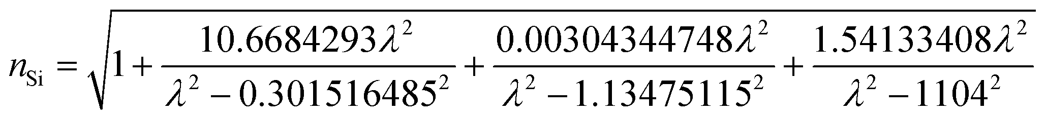
In order to obtain more accurate simulation results, we considered the dispersive properties of silicon as:50
| |
 | (4) |
where
λ is the wavelength of incident light in μm. The findings of the present work are based on previous experimental work,
38–40 in which the porosities of the PSi layers A and B were taken to be
P1 (=32%) and
P2 (=87%), respectively. The porosity range of the PSi layer from 32% to 87% has already been achieved and fabricated experimentally by the electrochemical etching of silicon wafer with the help of hydrogen fluoride as an electrolyte.
38
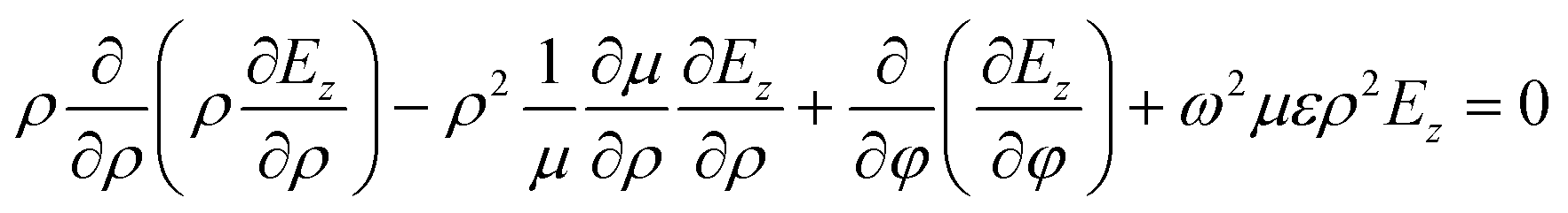
Now we considered the propagation of a cylindrical electromagnetic wave moving radially outward from the axis of symmetry, i.e., ρ = 0 (z axis), of the structure and coming out through cladding (i.e., Si substrate). This means we can omit the derivatives of the fields with respect to the z axis in the following wave equation corresponding to the TE mode in a cylindrical coordinate system as:28–30
| |
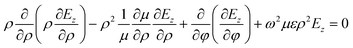 | (5) |
Eqn (5) can be solved by separation of the variables to get Ez, which is dependent on ρ and φ as:
| |
Ez(ρ, φ) = V(ρ)Φ(φ) =[CJm(kρ) + DYm(kρ)]exp(im![[thin space (1/6-em)]](https://www.rsc.org/images/entities/char_2009.gif) φ) φ)
| (6) |
where
Jm and
Ym are the Bessel and Neumann functions, respectively, corresponding to the azimuthal number
m. Here,

is the wavenumber of the propagating cylindrical electromagnetic wave inside a material of permittivity
ε and permeability
μ.
The azimuthal part of the magnetic field Hφ can be obtained using Maxwell's curl equation.
∇ × E = −jωμH as
| |
 | (7) |
here,

is the intrinsic impedance of the medium, and

are the first-order derivatives of the Bessel and Neumann functions, respectively.
30 The transfer matrix, which connects the electric and magnetic fields in the
jth layer of refractive index
nj at interfaces
ρj−1 and
ρj, is given as
28–30 (assuming
ρj−1 =
ρj):
| |
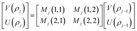 | (8) |
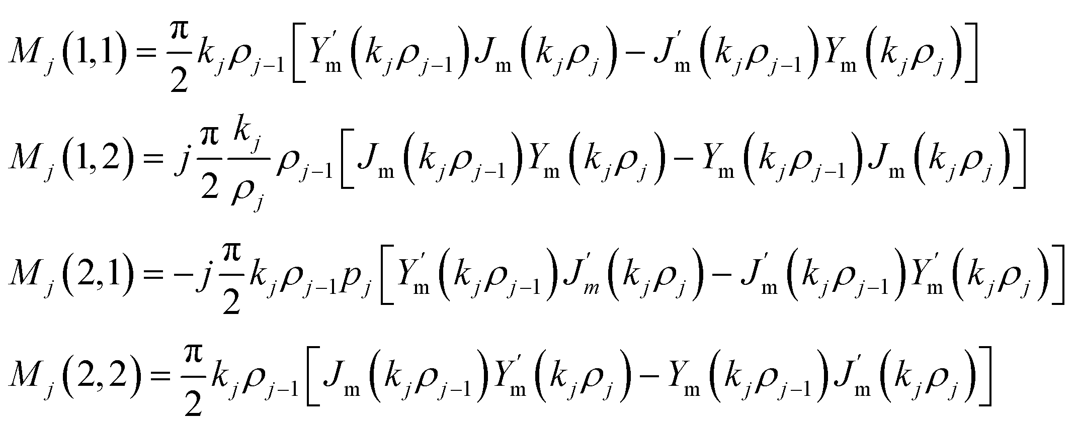
here, the elements of
Mj are given as:
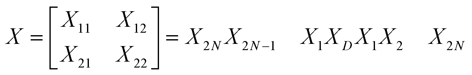
In order to find the total transfer matrix of the proposed structure [(AB)N/2D(AB)N/2/substrate], we have to consider the product of the transfer matrix of each cylindrical layer, as described below in accordance with Fig. 1.
| |
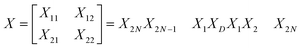 | (9) |
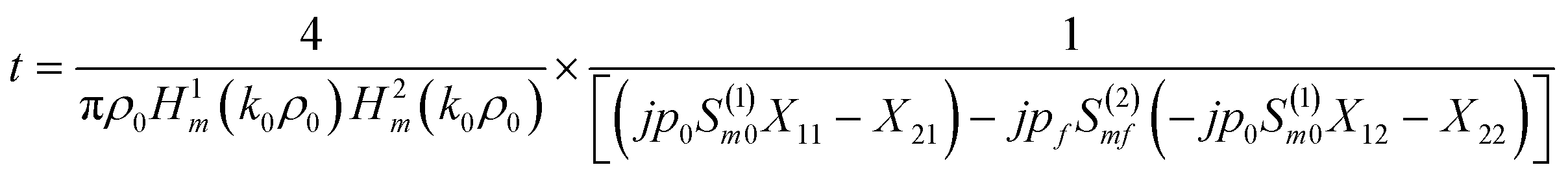
The transmission coefficient of the proposed 1D defective APC is given by:30
| |
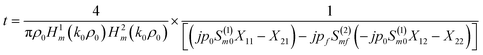 | (10) |
here
X11,
X12,
X21, and
X22 are the elements of the total transfer
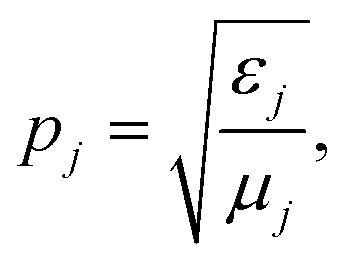
X. The admittances of the core and substrate layers are
p0 and
pf, respectively, and are given by

where
j takes the values of 0 and
f, corresponding to the core and substrate, respectively. The expression of
Sml is given as:
30| |
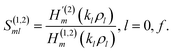 | (11) |
where
H(1)m,
H(2)m,

and

are the first and second kind of Hankel functions and their first-order derivatives, respectively. Finally the transmittance of the proposed 1D defective APC is obtained by:
3. Result and discussions
3.1. Determination of the effective refractive index of the PSi layers
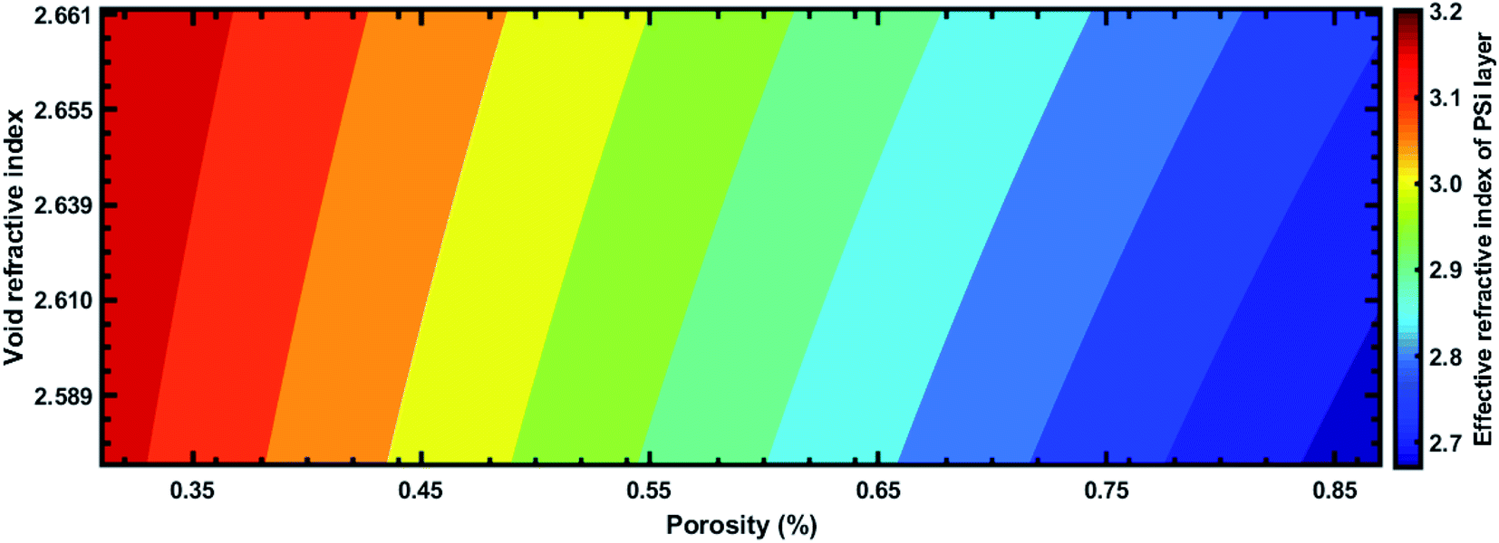
Braggeman's effective medium approach was applied in eqn (3) to obtain the porosity (P) and void refractive index (nv) dependent effective refractive index (neff) of the PSi layer. The porosities of the PSi layers chosen here were already determined and experientially realized in various previous research works.49,50 Thus the fabrication of our proposed sensor design based on the porosities of 34% and 87% of PSi layers was considered experimentally possible. The dependence of neff of the PSi layer on both P and nv both was plotted in a color map distribution, as shown in Fig. 2, with the help of MATLAB simulations. It is evident from Fig. 2 that the neff of the PSi layer increased with the increase in the refractive index of the material in the form of the liquid to be poured into the voids of the PSi layers at a particular value of P. On the other hand, neff decreased as we increased P from 0.30 to 0.87 at a given value of nv. The maximum value of neff was achieved corresponding to P = 30% at nv = 2.662, whereas the lowest value of neff was achieved with P = 87% at nv = 2.565. Thus increasing the refractive index of the voids increases the neff of the PSi layer, while increasing the porosity ratio decreases the neff of the PSi layer. This unique ability of controlling the neff of the PSi layer makes it suitable to be used in the designing of high-performance biophotonic sensors.
 |
| | Fig. 2 The color map distribution of the effective refractive index of the porous silicon layer (neff) dependent on the refractive index of void (nv) and porosity ratio (P). | |
3.2. Biophotonic sensor design
The proposed biophotonic sensor design, as shown in Fig. 1, is composed of two 1D APCs joined together through a cylindrical defect layer of air in which various blood serum samples have to be poured one by one for determining the creatinine concentration of each sample. Both the 1D APCs used in the proposed design consisted of binary layers of PSi of different porosities, as per the data given in Table 1.
Table 1 Details of the porous silicon material layers used in the proposed design
| Layer description |
Porosity (%) |
Thickness (μm) |
| First PSi layer (A) |
34 |
0.2 |
| Second PSi layer (B) |
87 |
0.6 |
The entire 1D defective APC structure is sandwiched between the hollow core of the radius ρ0 and the silicon cladding of the inner radius ρf, as shown in Fig. 1. The whole structure is surrounded by air. The analyte (blood serum sample whose creatinine concentration is to be determined) is allowed to flow over the top surface of the proposed design so that the air inside the pores of PSi layers is replaced by blood serum samples of various creatinine concentrations while the defect layer region is also filled with the same blood serum sample in accordance with Table 2. The purpose of selecting the porosity ratio of the PSi layers A and B of both APCs as 34% and 87%, respectively, was to get the maximum refractive index contrast, as shown in Fig. 2, which is an essential requirement for getting larger PBG in the operating wavelength range of the incident electromagnetic spectrum between 2000 and 2600 nm. A large PBG is an essential requirement for the better performance of the proposed biosensor design, as it allows the defect mode to be modulated within this PBG so that a variety of samples with minute variations in the concentration of creatinine can be examined. It is necessary take a special precaution while pouring blood serum into the pores of PSi layers in that the pressure of the blood serum sample fluid should be kept as low as possible to prevent any internal damage to the PSi layers.38
Table 2 Creatinine concentration in various blood serum samples and their refractive indices
| Creatinine blood cerium concentration (μmol L−1) |
Refractive index (nd) (RIU) |
| 80.90 |
2.661 |
| 81.43 |
2.655 |
| 82.30 |
2.639 |
| 83.30 |
2.610 |
| 84.07 |
2.589 |
| 85.28 |
2.565 |
3.3. Numerical results
Herein the period number was chosen as N = 18 for the 1D defective APC configuration [(AB)N/2D(AB)N/2/Substrate]. The core radius ρ0 was taken to be 10 mm, which is very large compared to the thickness of the individual layers of the defective APC structure. The large value of ρ0 ensures that the behavior of the APCs is similar to that of the planar PCs at normal incidence. In this study, the azimuthal number m was set to 0 and only normal incidence is thus discussed to overcome the difficulties that can arise at the time of characterization corresponding to the normal incidence.
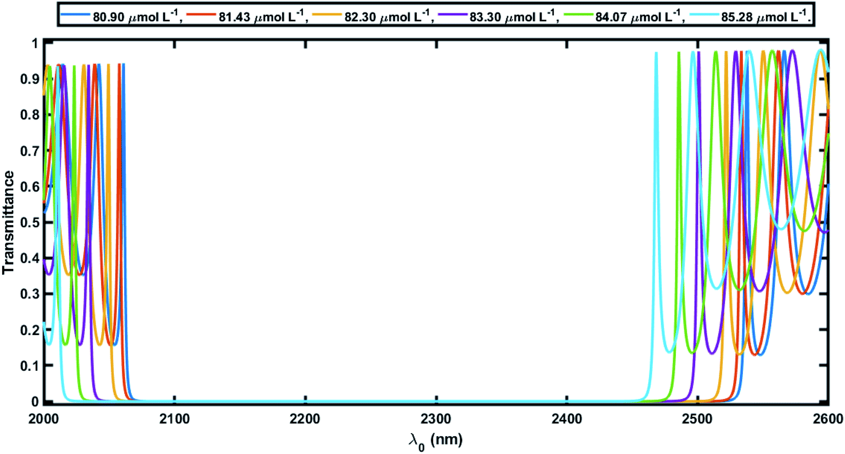
In order to elaborate, for the numerical results showing the performance of the 1D defective APC structure, we studied the transmission spectra of perfect periodic and defective APCs, as shown in Fig. 3 and 4, respectively. Fig. 3 shows six wide PBGs of zero transmission in the short wavelength of the infrared region of the electromagnetic spectrum corresponding to six blood serum samples of various creatinine concentrations in accordance with Table 2. These six samples of blood serum were poured into the voids of both PSi layers of an APC without defects, one by one separately. It could also be observed in Fig. 3 that as the creatinine concentration in the blood serum sample increased from 80.9 μmol L−1 to 85.28 μmol L−1 (as per the data given in Table 2), the higher and lower band edges (λh and λl, respectively) of all the six PBGs were shifted toward the lower wavelength side with almost a constant PBG width (Δλ = λh – λl) (Table 3). This is due to reason that the effective refractive index of the PSi layer of porosity ratio 34% had a high value of 3.2 and was almost constant, whereas the neff of the PSi layer of porosity ratio 87% varied between 2.8 to 2.68, depending on the refractive index of the blood serum samples of different creatinine concentrations, as evident in Fig. 2. This P and nv dependent behavior of the neff of the PSi layer changed the refractive index constant between the PSi layers of the structure. This change in the refractive index contrast between the PSi layers was compensated by shifting the respective PBG toward the lower wavelength side.
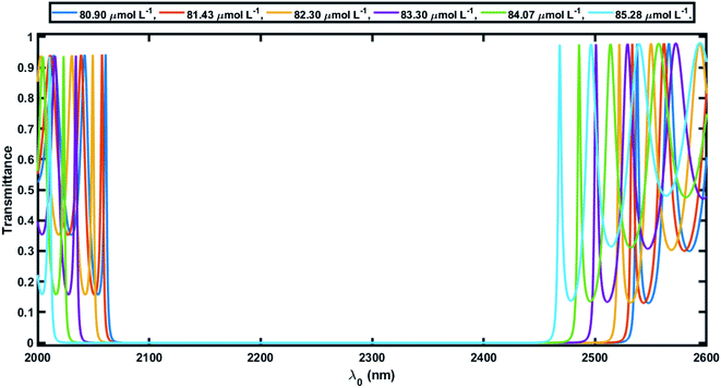 |
| | Fig. 3 The transmission spectra of 1D APC [(AB)18/Si] as a function of the wavelength corresponding to six different blood serum samples of creatinine concentration 80.9, 81.43, 82.3, 83.3, 84.07, and 85.28 μmol L−1 at normal incidence. Here, A and B represent PSi layers of porosity ratios 34% and 87%, respectively. | |
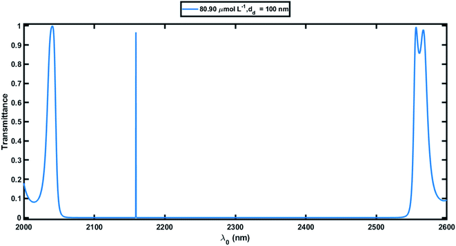 |
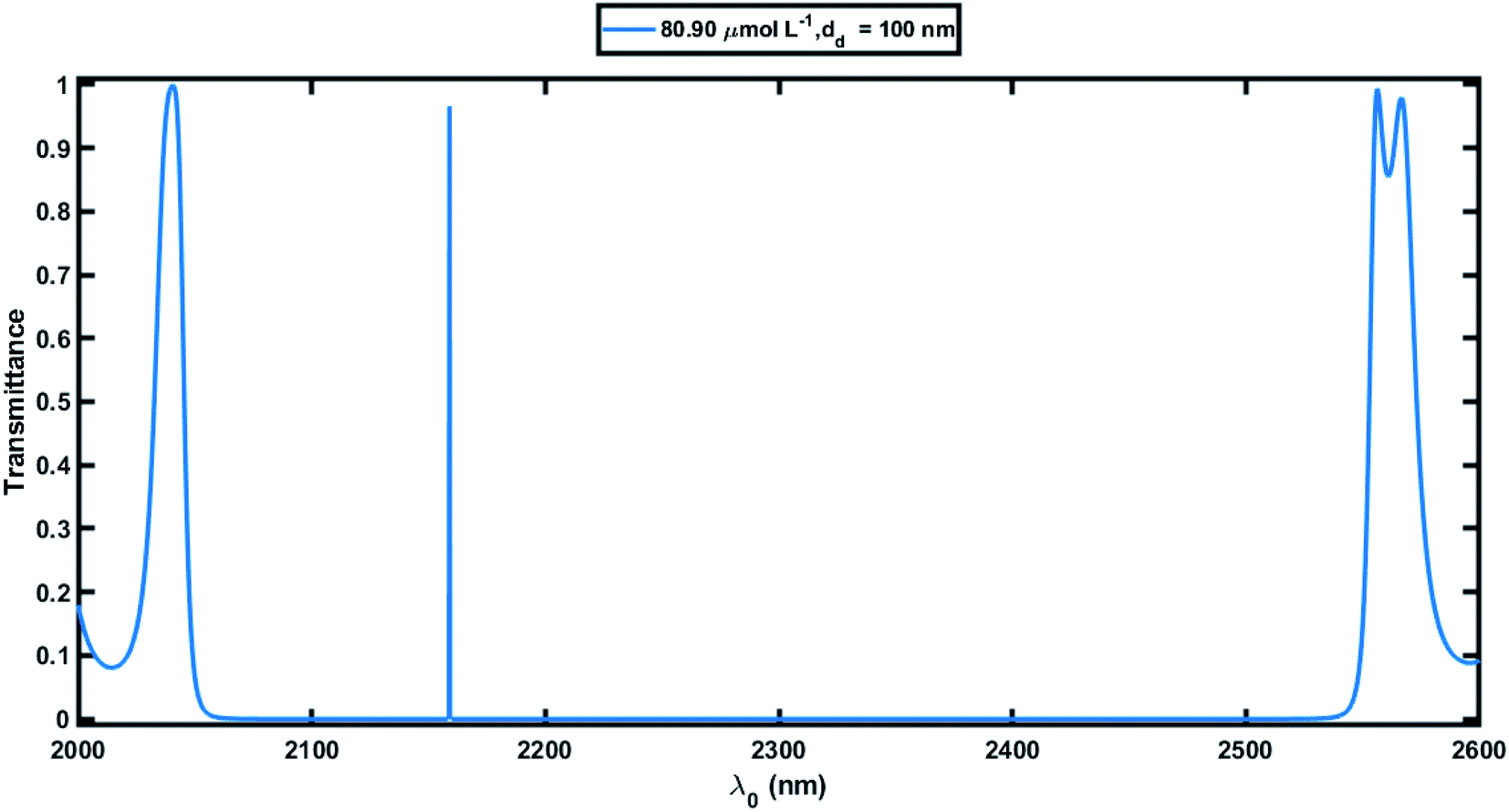
| | Fig. 4 The transmission spectra of 1D defective APC [(AB)9/D/(AB)9/Si] as a function of the wavelength corresponding to the blood serum sample of creatinine concentration 80.9 μmol L−1 at normal incidence. Here, D represents a defect layer of thickness dd = 100 nm. | |
Table 3 PBGs of the biophotonic sensor loaded with various blood serum samples (θ0 = 0°)
| Creatinine blood serum concentration (μmol L−1) |
Lower edge of PBG λl (nm) |
Higher edge of PBG λr (nm) |
Width of PBG Δλ = λh − λl (nm) |
| 80.90 |
2082 |
2509 |
427 |
| 81.43 |
2079 |
2504 |
425 |
| 82.30 |
2070 |
2493 |
423 |
| 83.30 |
2055 |
2472 |
417 |
| 84.07 |
2044 |
2456 |
412 |
| 85.28 |
2032 |
2439 |
407 |
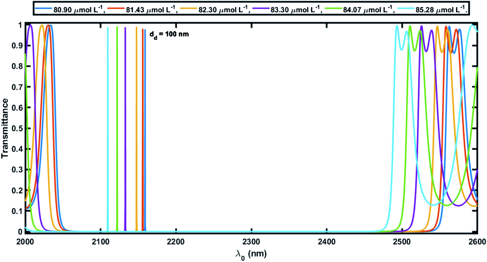
Next, we studied the transmission spectra of the 1D defective APC's structure [(AB)N/2/D/(AB)N/2/substrate] at normal incidence, as shown in Fig. 4. Here the defect region of width dd = 100 nm was filled with the blood serum sample of creatinine concentration 80.90 μmol L−1. The transmission spectra showed a transmission peak of intensity 96.59% located at 2159 nm within the PBG of the defective APC, which was almost the same as observed in Fig. 3. Further the blood serum samples of different creatinine concentrations in accordance with Table 2 were poured into the voids of the PSi layers as well as in the defect layer region of the structure one by one, and we observed the effects of these samples on the intensity and location of the defect mode inside the PBG. It can be noticed in Fig. 5 that as the creatinine concentration in the blood serum samples increased, the PBG edges and position of the defect mode inside the PBG corresponding to each sample were shifted toward the lower wavelength side due to the decrease in the reflective index contrast between both PSi layers of the structure (Fig. 2). Thus all the wavelengths of the incident radiation which lie inside the PBG were completely prohibited, except the wavelength corresponding to the defect mode. The mobility of the defect mode inside the PBG, due to each blood serum sample, could also be interpreted by the concept of standing waves as Δ = pλ = Neffγ. Here, the symbols Δ, p, Neff, and γ are used to represent the optical path difference, an integer, the effective refractive index of the cavity region, and the geometrical path difference, respectively. The proposed biosensor exhibited a sensitivity of about 464.2 nm per RIU at normal incidence, corresponding to a defect layer thickness dd = 100 nm, which is reasonably higher than the planar photonic crystal-based biosensor with a sensitivity of 306.25 nm per RIU proposed by Aly et al. at an oblique incidence of 85°.55 Moreover, the Q factor, FOM, and LOD of the proposed biosensor were 1.28 × 10⁵, 3.06 × 10⁴, and 4.14 × 10⁻⁶, respectively(at θ0 = 0°).
 |
| | Fig. 5 The transmission spectra of 1D defective APC [(AB)9/D/(AB)9/Si] as a function of the wavelength corresponding to six different blood serum samples of creatinine concentration 80.9, 81.43, 82.3, 83.3, 84.07, and 85.28 μmol L−1 at normal incidence. Here, D represents a defect layer of thickness dd = 100 nm. | |
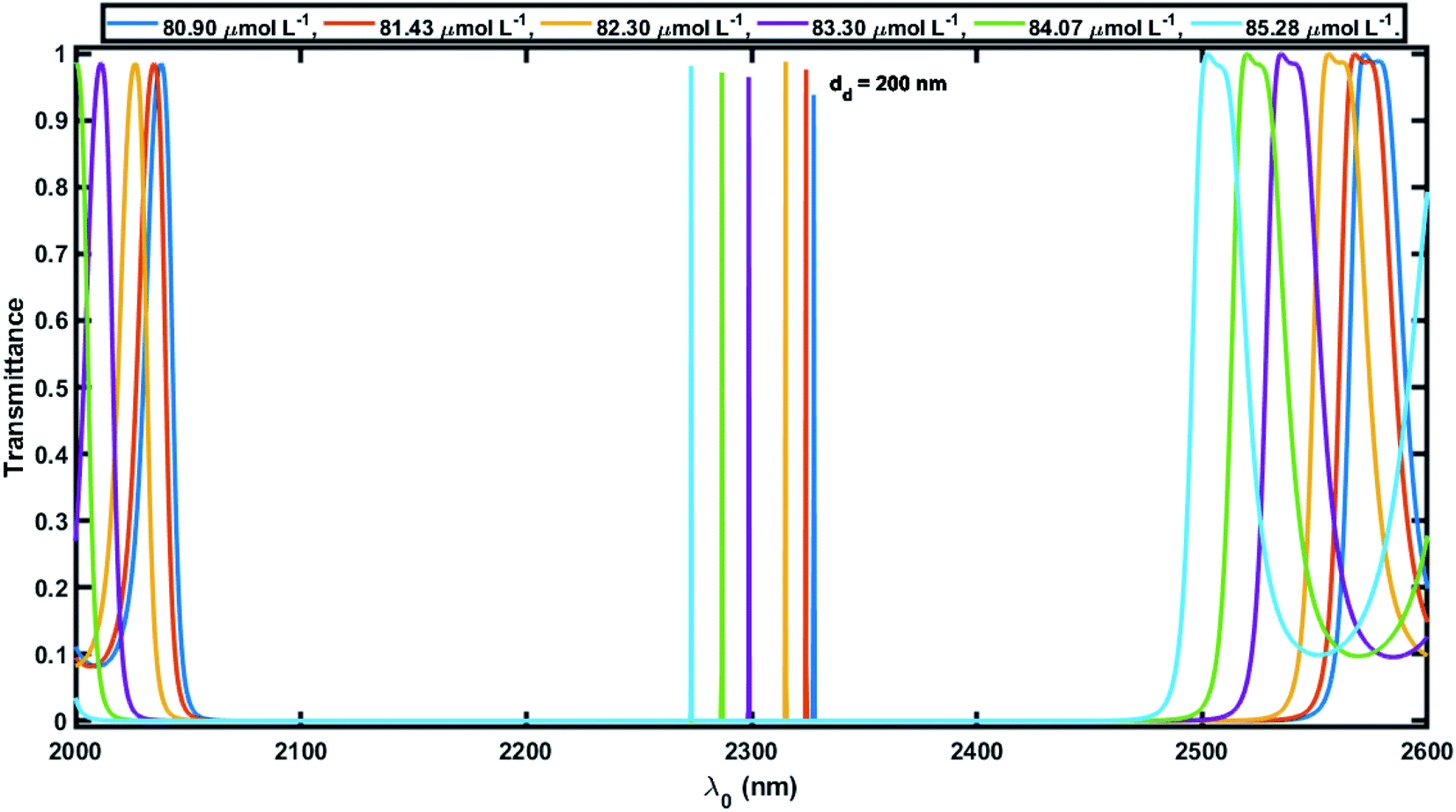
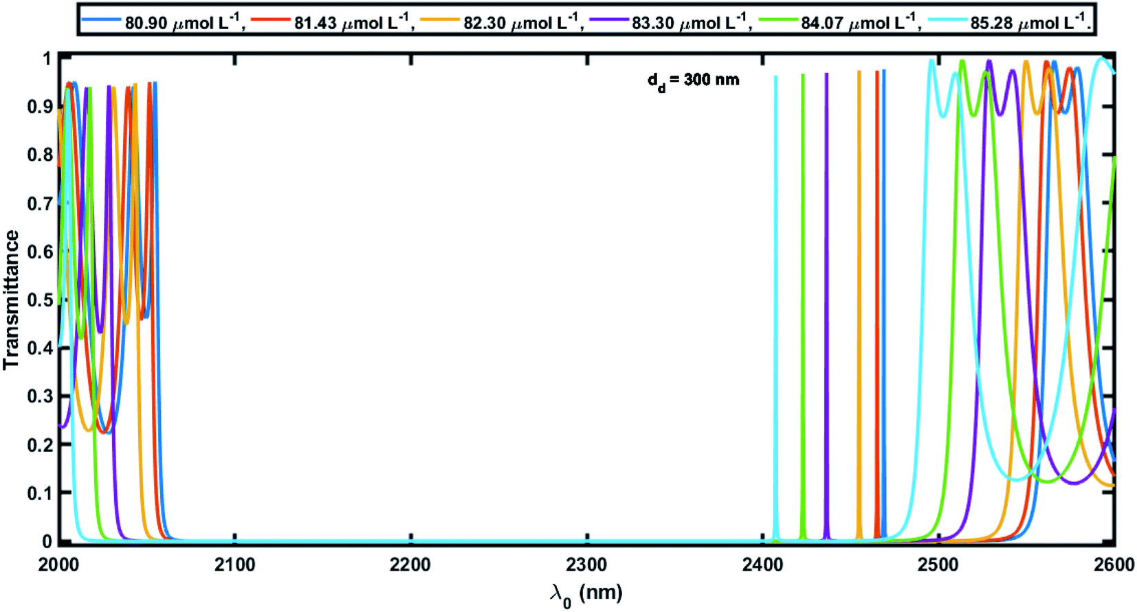
Next, efforts were made to increase the sensitivity of the proposed biosensor further by increasing the thickness of the defect layer. The increase in the thickness of the defect layer (dd) also increased the geometrical path difference, which in turn improved the sensitivity. Fig. 6 and 7 show the transmission spectra of the proposed biosensor corresponding to defect layer thicknesses of 200 nm and 300 nm, respectively, at normal incidence, displaying that the increase in the thickness of the defect layer region causes the positions of the respective defect modes to shift to the higher wavelength side. This increase in the thickness of the defect layer region also alters the amplitude of each defect mode slightly. Due to the increase in dd = 100 nm to 200 nm, the average sensitivity was raised from 464.2 nm per RIU to 525.90 nm per RIU, respectively. The sensitivity of the proposed biosensor attained a maximum value of 638.90 nm per RIU corresponding to a value of dd of 300 nm. Further increasing the value of dd resulted in a decrease in the sensitivity of the proposed design. Moreover the proposed biosensor design with various blood serum samples exhibited an efficient average sensitivity of around 638.90 nm per RIU at normal incidence. Thus the sensitivity of our structure is more than twice the sensitivity of 305.25 nm per RIU at 85° incident angle achieved by Aly et al.55 in their design composed of a 1D planar PC.
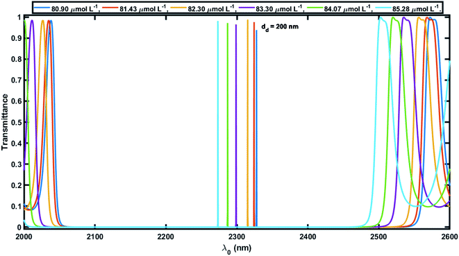 |
| | Fig. 6 The transmission spectra of 1D defective APC [(AB)9/D/(AB)9/Si] as a function of the wavelength corresponding to six different blood serum samples of creatinine concentration 80.9, 81.43, 82.3, 83.3, 84.07, and 85.28 μmol L−1 at normal incidence. Here, D represents a defect layer of thickness dd = 200 nm. | |
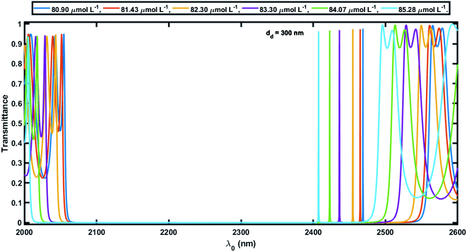 |
| | Fig. 7 The transmission spectra of 1D defective APC [(AB)9/D/(AB)9/Si] as a function of the wavelength corresponding to six different blood serum samples of creatinine concentration 80.9, 81.43, 82.3, 83.3, 84.07, and 85.28 μmol L−1 at normal incidence. Here, D represents a defect layer of thickness dd = 300 nm. | |
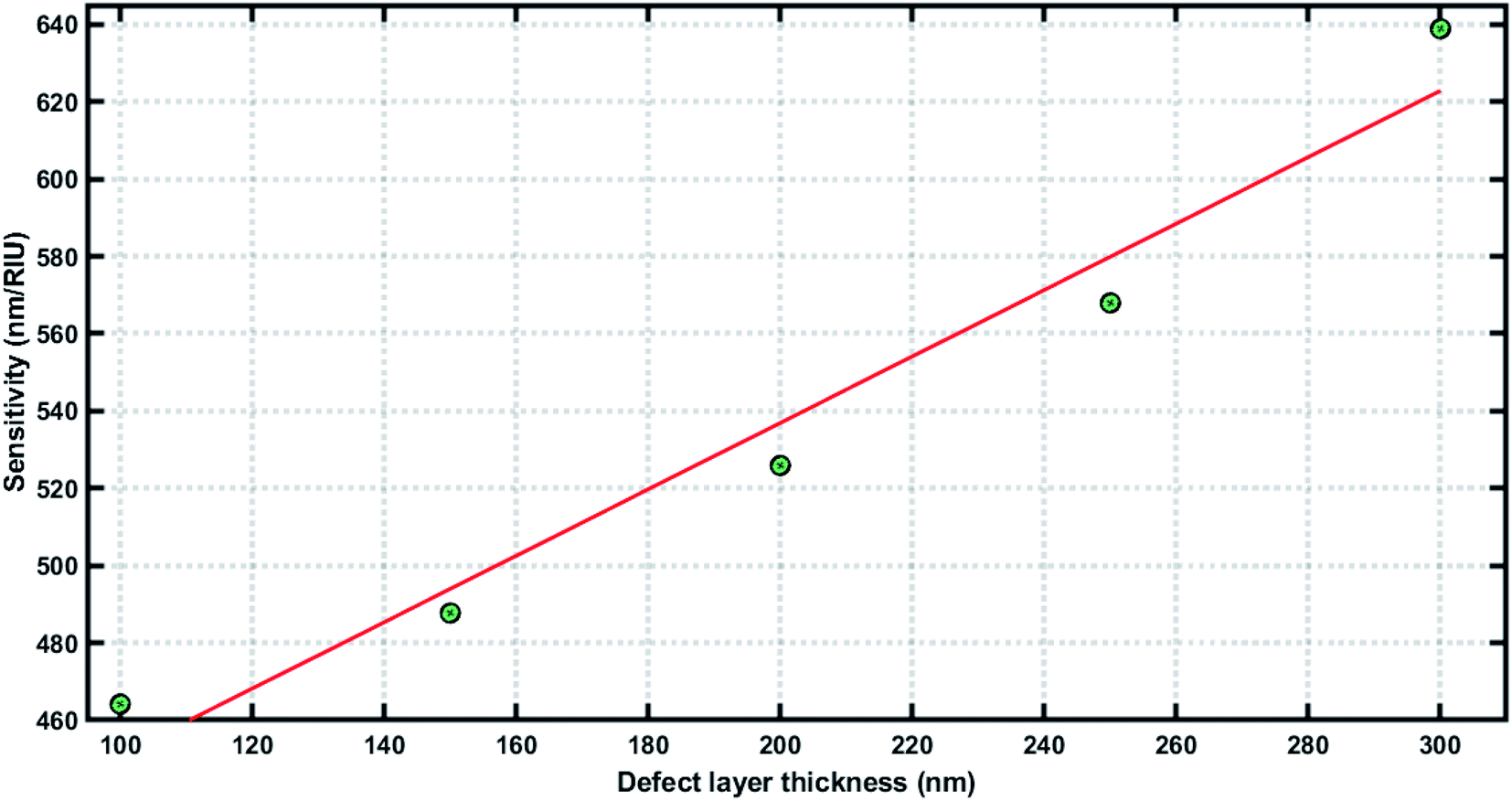
Fig. 8 shows how the average sensitivity (nm per RIU) of the proposed design varied with the thickness of the defect layer (dd) region. It was seen that the sensitivity increased with dd and followed the linear filling equation S = 0.8594dd + 365.04. Here, the square of the correlation factor (R2) between the linear curve fitting and simulated data was 0.9618. The calculated R2 was 0.9618, which indicates a high linearity of the proposed biosensor in comparison with the recent work by Aly et al.,55 where they reported R2 = 0.93967. Moreover, the value of dd was optimized at 300 nm as the maximum, because further increases in the value of dd disturbed the performance of the proposed biosensor due to the appearance of more new peaks inside the PBG.
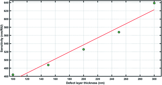 |
| | Fig. 8 Sensitivity (S) of the proposed 1D defective APC-based biosensor as a function of the defect layer thickness (dd). | |
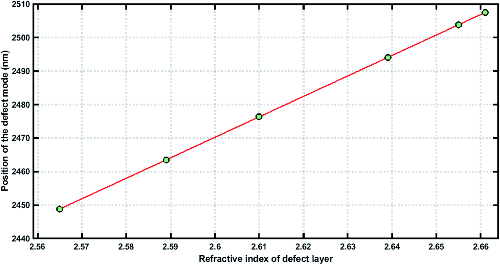
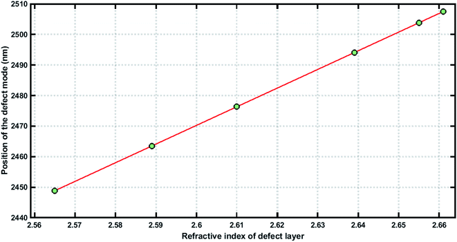
Further, we also analyzed the dependence of the defect mode position as a function of the refractive index value of the defect layer (nd), which was the same as nv in the proposed design. The position of each defect mode inside the respective PBG increased linearly with increasing the refractive index of the blood serum sample poured into the voids of the PSi layers and also into the defect layer region (nd = nv) of the structure. The linear fitting between the refractive index of the blood serum samples (nd = nv) and the respective position of the defect mode inside their PBGs are presented in Fig. 9. The linear fitting of the simulated data of the proposed biosensor [(AB)N/2/D/(AB)N/2/Substrate] can be given according to the following equation.
| λdefect (nm) = 64nd (RIU) + 760, (R2 = 0.9999) |
 |
| | Fig. 9 The defect mode position of the 1D defective APC-based biosensor as a function of the defect layer refractive indices corresponding to six different blood serum samples of creatinine concentration 80.9, 81.43, 82.3, 83.3, 84.07, and 85.28 μmol L−1 inside their respective PBGs at normal incidence. | |
3.4. Analysis of the performance of the biophotonic sensor under optimum conditions
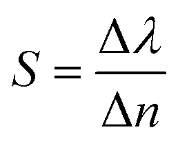
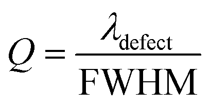
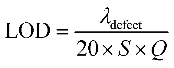
From the above discussions, the optimum conditions are N = 18, dd = 300 nm, and θ0 = 0°. In order to illustrate the performance of our proposed biosensor composed of 1D defective APC in the presence of various blood serum samples of different concentrations, we calculated the S, Q factor, FOM, and LOD values of our biophotonic sensor. These parameters are very important for evaluating the efficiency and performance of any biosensor. The parameters can easily be obtained with the help of the following expressions:49,50
Sensitivity,
| |
 | (13) |
Quality factor,
| |
 | (14) |
Figure of merit,
| |
 | (15) |
Limit of detection,
| |
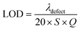 | (16) |
where the refractive index of the blood serum sample (
nd =
nv = 2.661 RIU) at a creatinine concentration of 80.90 μmol L
−1 and the corresponding peak wavelength of the defect mode were used as references to obtain Δ
λ and Δ
n for various blood serum samples, where Δ
λ =
λdefect (corresponding to each sample) −
λdefect (at 80.9 μmol L
−1) and Δ
n =
nd (corresponding to each sample) −
nd (at 80.9 μmol L
−1). Here, FWHM represents the full width of half maximum of the defect at that mode.
Table 4 summarizes all the above data for the proposed biosensor corresponding to dd = 300 nm at θ0 = 0°. The sensitivity of the proposed biosensor ranged from 637.73 nm per RIU to 640.29 nm per RIU, corresponding to the sample with a creatinine concentration between 81.43 and 85.28 μmol L−1 under consideration. The average sensitivity of the proposed 1D defective APC structure [(AB)N/2/D/(AB)N/2/Substrate] was about 638.90 nm per RIU. Thus, the proposed biosensor design was capable of measuring the change in the refractive index of many body fluids effectively and provided a high value of sensitivity as compared to many sensor designs reported earlier.53–55 The Q factor and FOM of our design varied between (1.51 to 0.75) × 105 and (2.60 to 1.961) × 104 RIU, corresponding to samples of creatinine concentration varying from 80.90 to 85.28 μmol L−1, respectively.
Table 4 Biophotonic sensor analysis loaded with different blood serum samples
| Creatinine blood serum concentration (μmol L−1) |
n (RIU) |
Peak wavelength (nm) |
S (nm per RIU) |
FWHM (nm) |
Q × 105 |
FOM × 104 (RIU) |
| 80.90 |
2.661 |
2468.7497 |
— |
0.0164 |
1.51 |
— |
| 81.43 |
2.655 |
2464.9233 |
637.7333 |
0.0245 |
1.01 |
2.60 |
| 82.30 |
2.639 |
2454.7113 |
638.1091 |
0.0245 |
1.00 |
2.60 |
| 83.30 |
2.610 |
2436.1679 |
638.8588 |
0.0246 |
0.99 |
2.60 |
| 84.07 |
2.589 |
2422.7019 |
639.5528 |
0.0245 |
0.99 |
2.61 |
| 85.28 |
2.565 |
2407.2818 |
640.2906 |
0.0327 |
0.74 |
1.96 |
Finally, the LOD of the proposed biosensor was calculated with the help of eqn eqn (16). The value of the LOD varied between (1.92 to 2.55) × 10−6 RIU, corresponding to a sample of concentration 80.80 to 85.28 μmol L−1. This value is very low as per desire, which makes our biosensor capable of resolving very small changes in the refractive index of samples in which we want to find the creatinine concentration in the blood serum of the patient to be investigated. Moreover, Table 5 compares the findings of the proposed 1D defective APC-based biophotonic sensing designs with the previous works based on 1D defective planar photonic crystals recently carried out by various research groups worldwide. This comparison highlights how the APC-based designs may be a better alternative for high-performance biophotonic sensors at normal incidence, which is not possible with conventional 1D defective planar photonic designs at normal incidence. It is evident from Table 5 that the proposed biosensor possessed high sensitivity and a much better performance in contrast to the recent research works mentioned in Table 5.
Table 5 Comparison of the numeric values for the sensitivity, FOM, and LOD of the proposed design with previous designs for evaluating the performance of the proposed biophotonic sensor design using a 1D defective APC structure
| Year |
S (nm per RIU) |
FOM (RIU) |
LOD × 10−6 |
Frequency range |
Ref. |
| 2017 |
180 |
— |
— |
Near infrared (NIR) |
56 |
| 2019 |
25.7–45.06 |
— |
— |
NIR |
57 |
| 2019 |
42–43 |
— |
— |
NIR |
58 |
| 2020 |
306.25 |
(1.5–10.3) × 104 |
1.04 |
Visible to NIR |
55 |
| 2021 |
71–75 |
— |
— |
NIR |
59 |
| 2021 |
51–150.6 |
153.5–14036.8 |
— |
Visible |
60 |
| This work |
637–640.3 |
(1.96–2.6) × 104 |
(1.9–2.6) |
NIR |
— |
4. Conclusion
In this study, we successfully investigated and theoretically developed a high-sensitivity biophotonic sensor capable of sensing creatinine concentration in various blood serum samples. The proposed design was composed of a 1D defective APC. The modified TMM approach was applied to investigate the performance of the biosensor at normal incidence. The biosensing technique of this sensor utilized the tuning of the defect mode inside the PBG of the transmission spectra of the 1D defective APC at normal incidence depending upon various blood serum samples. The maximum sensitivity of 640.29 nm per RIU at 85.28 μmol L−1 was found with the optimum value of the defect layer of thickness of 300 nm, which has not been achieved in ordinary photonic sensors at normal incidence. The proposed idea may be explored to develop various biosensor designs capable of investigating various body fluids for getting instant and accurate results in medical science.
Conflicts of interest
There are no conflicts to declare.
References
- J. D. Joannopoulos, S. G. Johnson, J. N. Winn and R. D. Meade, Photonic Crystals: Molding the flow of Light, Princeton University Press, 2008, pp. 1–22 Search PubMed
 .
. - J. C. Knight, J. Broeng, T. A. Birks and P. S. J. Russell, Science, 1998, 282, 1476–1478 CrossRef CAS PubMed .
- C. M. Bowden, J. P. Dowling and H. O. Everitt, J. Opt. Soc. Am. B, 1993, 10, 280 CrossRef .
- S. K. Awasthi, A. Mishra, U. Malaviya and S. P. Ojha, Solid State Commun., 2008, 146, 506–509 CrossRef CAS .
- S. K. Awasthi, Indian J. Phys., 2021 DOI:10.1007/s12648-020-01939-5 .
- S. K. Awasthi, R. Panda and L. Shiveshwari, Phys. Plasmas, 2017, 24, 072111 CrossRef .
- L. Shiveshwari and S. K. Awasthi, Phys. B, 2020, 597, 412360 CrossRef CAS .
- E. Yablonovitch, Phys. Rev. Lett., 1987, 58, 2059–2062 CrossRef CAS .
- S. John, Phys. Rev. Lett., 1987, 58, 2486–2489 CrossRef CAS PubMed .
- S. K. Awasthi, R. Panda and L. Shiveshwari, Phys. Plasmas, 2018, 25, 052103 CrossRef .
- S. K. Awasthi, U. Malaviya and S. P. Ojha, J. Opt. Soc. Am. B, 2006, 23, 2566–2571 CrossRef CAS .
- A. Nagaty, A. Mehaney and A. H. Aly, Chin. Phys. B, 2018, 27, 094301 CrossRef .
- A. H. Aly, H. A. Elsayed and C. Malek, Opt. Appl., 2018, 48, 53–64 CAS .
- A. Mishra, S. K. Awasthi, P. Singh, U. Malaviya and S. P. Ojha, J. Mod. Opt., 2012, 59, 601–610 CrossRef .
- A. H. Aly, H. A. Elsayed, A. A. Ameen and S. H. Mohamed, Int. J. Mod. Phys. B, 2017, 31, 1750239 CrossRef CAS .
- S. R. Qutb, A. H. Aly and W. Sabra, Int. J. Mod. Phys. B, 2021, 35, 2150012 CrossRef CAS .
- S. E. S. Abd El-Ghany, W. M. Noum, Z. S. Matar, Z. A. Zaky and A. H. Aly, Phys. Scr., 2020, 96, 035501 CrossRef .
- A. Mehaney, A. Nagaty and A. H Aly, J. Supercond. Novel Magn., 2018, 31, 4173–4177 CrossRef .
- A. H. Aly and A. Mehaney, Indian J. Phys., 2017, 91, 1021–1028 CrossRef CAS .
- A. H. Aly and H. A. El Sayed, J. Mod. Opt., 2017, 64, 871–877 CrossRef .
- A. H. Aly and Z. A. Zaky, Cryogenics, 2019, 104, 102991 CrossRef CAS .
- M. Yunianto, A. N. Permata, D. Eka, D. Ariningrum, S. Wahyuningsih and M. Ahmad, Mater. Sci. Eng., 2017, 176, 012014 Search PubMed .
- N. Ayyanar, G. T. Raja, M. Sharma and D. S. Kumar, IEEE Sens. J., 2018, 18, 7093–7099 CAS .
- J. Raveendran, P. E. Resmi, T. Ramachandran, B. G. Nair and T. G. Satheesh Babu, Sens. Actuators, B, 2017, 243, 589–595 CrossRef CAS .
- A. H. Aly, S. M. Shaban and A. Mehaney, Appl. Opt., 2021, 60, 3224–3231 CrossRef PubMed .
- A. H. Aly, A. Nagaty, Z. Khalifa and A. Mehaney, J. Appl. Phys., 2018, 123, 185102 CrossRef .
- H. Kurt and D. S. Citrin, Opt. Express, 2005, 25, 10316–10326 CrossRef .
- A. A. Ameen, H. ElSayed and A. H. Aly, RSC Adv., 2021, 11, 14915–14921 RSC .
- V. V. Nikolaev, G. S. Sokolovskii and M. A. Kaliteevskii, Semiconductors, 1999, 33, 147–152 CrossRef CAS .
- C.-A. Hu, C.-J. Wu, T.-J. Yang and S. L. Yang, Opt. Commun., 2013, 291, 424–434 CrossRef CAS .
- M. A. Kaliteevski, R. A. Abram, V. V. Nikolaev and G. S. Sokolovski, J. Mod. Opt., 1999, 46, 875–890 CrossRef CAS .
- X. Sun and A. Yariv, Opt. Express, 2007, 15, 17323–17333 CrossRef PubMed .
- S. K. Srivastava and A. Aghajamali, Phys. B, 2016, 489, 67–72 CrossRef CAS .
- J. Scheuer, W. M. J. Green, G. A. DeRose and A. Yariv, IEEE J. Sel. Top. Quantum Electron., 2005, 11, 476–484 CAS .
- T.-W. Chang, H.-T. Hsu and C.-J. Wu, J. Electromagn. Waves Appl., 2011, 25, 2222–2235 CrossRef .
- L. Jiang and X. Li, Optik, 2016, 127, 916–919 CrossRef CAS .
- A. E. Khalil, A. H. El-Saeed, M. A. Ibrahim, M. E. Hashish, M. R. Abdelmonem, M. F. O. Hameed, M. Y. Azab and S. S. A. Obayya, Opt. Quantum Electron., 2018, 50(158), 1–12 CAS .
- A. Mehaney, M. M. Abadla and H. A. Elsayed, J. Mol. Liq., 2021, 322, 114978 CrossRef CAS .
- M. M. Abadla, H. A. Elasyed and A. Mehaney, Phys. E, 2020, 119, 1140201 CrossRef .
- P. Mehrotra, J. Oral Biol. Craniofacial Res., 2016, 6, 153–159 CrossRef .
- A. Zaky and A. H. Aly, Appl. Opt., 2021, 60, 1411–1419 CrossRef PubMed .
- M. El Beheiry, V. Liu, S. Fan and O. Levi, Opt. Express, 2010, 18, 20702–22714 CrossRef PubMed .
- S. Kim, J. Lee, H. Jeon and H. J. Kim, Appl. Phys. Lett., 2009, 94, 133503 CrossRef .
- V. S. Y. Lin, K. Motesharei, K. P. S. Dancil, M. J. Sailor and M. R. Ghadiri, Science, 1997, 278, 840–843 CrossRef CAS PubMed .
- K. V. Sreekanth, S. Zeng, K. T. Yong and T. Yu, Sens. Actuators, B, 2013, 182, 424–428 CrossRef CAS .
- C. P. Verma, K. Asokan, P. K. Kanaujia, M. Adnan, D. Kanjilal and G. V. Prakash, Appl. Surf. Sci., 2020, 535, 147696 CrossRef .
- S. A. Jenie, S. Pace, B. Sciacca, R. D. Brooks, S. E. Plush and N. H. Voelcker, ACS Appl. Mater. Interfaces, 2014, 6, 12012–12021 CrossRef CAS .
- R. J. Martin-Palma, V. Torres-Costa, M. Arroyo-Hernández, M. Manso, J. Pérez-Rigueiro and J. M. Martinez-Duart, Microelectron. J., 2004, 35, 45–48 CrossRef CAS .
- A. M. Ahmed and A. Mehaney, Sci. Rep., 2019, 9, 6973 CrossRef .
- Z. A. Zaky, A. M. Ahmed, A. S. Shalaby and A. H. Aly, Sci. Rep., 2020, 10, 9736 CrossRef CAS PubMed .
- V. A. Pedrosa, J. Yan, A. L. Simonian and A. Revzin, Electroanalysis, 2011, 23, 1142–1149 CrossRef CAS .
- S. Pineda, Z. J. Han and K. Ostrikov, Materials, 2014, 7, 4896–4929 CrossRef CAS PubMed .
- Z. Chen, M. Lu, D. Zou and H. Wang, J. Environ. Sci., 2012, 24, 541–549 CrossRef CAS .
- W. Junge, B. Wilke, A. Halabi and G. Klein, Clin. Chim. Acta, 2004, 344, 137–148 CrossRef CAS .
- A. H. Aly, D. Mohamed, M. A. Mohaseb, N. S. Abd El-Gawaad and T. Trabelsi, RSC Adv., 2020, 10, 31765–31772 RSC .
- M. H. Haron, A. R. MdZain and B. Y. Majlis, IEEE Reg. Symp. Micro Nanoelectron., 2017, 116–117 Search PubMed .
- H. J. El-Khozondar, P. Mahalakshmi, R. J. El-Khozondar, N. R. Ramanujam, I. S. Amiri and P. Yupapin, Phys. E, 2019, 111, 29–36 CrossRef CAS .
- N. R. Ramanujam, I. S. Amiri, S. A. Taya, S. Olyaee, R. Udaiyakumar, A. Pasumpon, K. S. Joseph Wilson, P. Mahalakshmi and P. P. Yupapin, Microsyst. Technol., 2019, 25, 189–196 CrossRef .
- A. Bijalwan, B. K. Singh and V. Rastogi, Optik, 2021, 226, 165994 CrossRef CAS .
- K. M. Abohassan, H. S. Ashour and M. M. Abadla, RSC Adv., 2021, 11, 12058–12065 RSC .
|
| This journal is © The Royal Society of Chemistry 2021 |
Click here to see how this site uses Cookies. View our privacy policy here. 
 Open Access Article
 This Open Access Article is licensed under a Creative Commons Attribution-Non Commercial 3.0 Unported Licence
 *a and
Arafa H. Alyb
*a and
Arafa H. Alyb


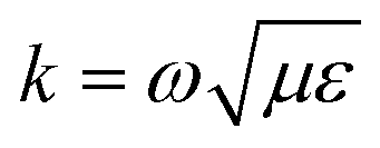 is the wavenumber of the propagating cylindrical electromagnetic wave inside a material of permittivity ε and permeability μ.

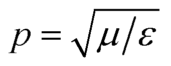 is the intrinsic impedance of the medium, and
  are the first-order derivatives of the Bessel and Neumann functions, respectively.30 The transfer matrix, which connects the electric and magnetic fields in the jth layer of refractive index nj at interfaces ρj−1 and ρj, is given as28–30 (assuming ρj−1 = ρj):
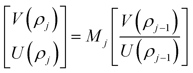

 where j takes the values of 0 and f, corresponding to the core and substrate, respectively. The expression of Sml is given as:30
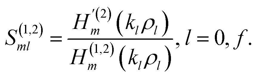
 and
and  are the first and second kind of Hankel functions and their first-order derivatives, respectively. Finally the transmittance of the proposed 1D defective APC is obtained by: