
 Open Access Article
 This Open Access Article is licensed under a Creative Commons Attribution-Non Commercial 3.0 Unported Licence
Tunable electronic and optical properties of a BAs/As heterostructure by vertical strain and external electric field
X. Q. Deng *,
R. Q. Sheng and
Q. Jing
*,
R. Q. Sheng and
Q. Jing
Hunan Provincial Key Laboratory of Flexible Electronic Materials Genome Engineering, Changsha University of Science and Technology, Changsha 410114, China. E-mail: xq_deng@163.com
First published on 21st June 2021
Abstract
Based on the first-principles method, we investigated the electronic properties of a BAs/arsenene (As) van der Waals (vdW) heterostructure and found that it has an intrinsic type-II band alignment with a direct band gap of 0.25 eV, which favors the separation of photogenerated electrons and holes. The band gap can be effectively modulated by applying vertical strain and external electric field, displaying a large alteration in the band gap via the strain and experiencing an indirect-to-direct band gap transition. Moreover, the band gap of the heterostructure varies almost linearly with external electric field, and the semiconductor-to-metal transition can be realized in the presence of a strong electric field. The calculated band alignment and optical absorption reveal that the BAs/As heterostructure could present an excellent light-harvesting performance. The absorption strength can be tuned mainly by interlayer coupling, while external electric field shows clear regulating effects on the absorption strength and absorption edge.
1. Introduction
Recently, small molecules1–4 and two-dimensional (2D) materials5–8 have attracted increasing attention because of their potential in next-generation electronic and photonic applications, such as organic light-emitting diodes (OLEDs),2 spin filtering effect (SFE),3 field effect transistors (FETs),6 and optoelectronic devices.8 2D materials display numerous intriguing physical properties that are distinct from those of their bulk phases as the electronic structure can be substantially altered. To modulate the electronic and optical properties of monolayers, numerous individual monolayers (MLs) with different bandgaps have been vertically stacked to fabricate a van der Waals (vdW) heterostructure,9–11 which may break through the limitation of a single material. In addition, some new physics may be achieved at their interface. For instance, a GeSe/phosphorene vdW p–n heterostructure was found to have an indirect band gap and the typical type-II heterostructure characteristic, facilitating the effective separation of electrons and holes between valence-band maximum (VBM) and conduction-band minimum (CBM) states.12 The arsenene stacked to C3N could present excellent light-harvesting performance, and the band gap of the heterostructure can be tuned via strain or external electric field.13 A boron arsenide (BAs) film, the emerging group V–VII compound,14 which has been deposited on the basal plane of hexagonal silicon carbide, is a direct gap material with a room temperature energy gap of about 1.4 eV. As a photoelectrode, boron arsenide was found to be photoactive under both visible light and UV-Vis irradiation.15 Moreover, BAs have an ultrahigh lattice thermal conductivity, κ, of over 2000 W m K−1 at room temperature (RT), which is comparable to that of diamond.16 Furthermore, it has been found that semihydrogenated BAs nanosheets are a promising bipolar magnetic semiconductor (BMS).17 Ullah et al. found that hydrogenated and fluorinated BAs are likely to have comparable stabilities, which can have applications in hydrogen storage devices and ultrafast electronic devices.18 The heterostructure consists of hydrogenated BAs and fluorinated BAs showing type-II semiconductor characteristics, in which the valence and conduction bands are composed of different layers,19 and the same type-II semiconductors can also be found in the SnC/BAs heterostructure.20 The electronic properties of the heterostructure, which consists of hexagonal boron phosphide (h-BP) and hexagonal boron arsenide (h-BAs), can be modulated effectively by an external electric field.21Since BAs and As have hexagonal lattice similar to graphene, what about the performance if we combine the vertical BAs/As heterostructure. In this study, using the first-principles method based on density functional theory (DFT) calculations, we investigated the equilibrium geometry of stable BAs/As heterostructure and electronic properties. The results demonstrate that it has a type-II band-alignment characteristic with a direct band gap of 0.25 eV, which facilitates the separation of electrons and holes. Moreover, the electronic and optical properties can be tuned by vertical strain and external electric field. These results suggest that the BAs/As heterostructures can be used as promising materials for developing novel devices.
2. Models and methods
The geometry optimizations and calculations of electronic properties are performed via the first-principles method based on density functional theory (DFT). All of the calculations are implemented in Atomistix ToolKit.22,23 We employed a Troullier–Martins norm-conserving pseudopotential to represent the atom core and linear combinations of atomic orbitals to expand the valence state of electrons. The convergence criteria for the ionic relaxation are such that the remnant force on each atom is below 0.01 eV Å−1. The exchange–correlation potential is described by the generalized gradient approximation (GGA).24 The equilibrium density matrix (DM) is evaluated by a contour integration method, while the nonequilibrium DM is numerically computed on a line with an imaginary part of 0.001 eV. The real space grid techniques are used with an energy cutoff of 150 Ry as the required cutoff energy in numerical integrations and the solution of the Poisson equation using a fast Fourier transform (FFT). The K-point sampling of the first Brillouin region is set as 11 × 11 × 1. A vacuum layer of 30 Å is set in the plane normal direction, which is sufficient to eliminate the cell-to-cell interactions. The DFT-D3 method25,26 of Grimme has obtained very good agreement with reliable theoretical or experimental results for the calibration results between two-dimensional layered materials. Therefore, we used Grimme DFT-D3 to correct vdW interactions between BAs and As.Four possible stacking orders of BAs/As have been considered, namely TB-, TAs-, HT-, and HB-stacking, as shown in Fig. 1(a)–(d). For TB-stacking and TAs-stacking, B (As) atoms in BAs are right above the top arsenic atoms of arsenene layer when the hexagonal rings of the two layers are aligned. HT-stacking corresponds to the top arsenic atom in the arsenene, which is located in the center of the hexagonal ring of the BAs layer. In contrast, when the bottom arsenic atom of the arsenene layer is in the center of the BAs hexagonal ring, it is marked HB-stacking. The optimized lattice parameters for BAs and As monolayers are 3.450 and 3.615 Å, respectively, and the buckling height of arsenene is 1.4 Å. The 3 × 3 × 1 cell for both BAs and As monolayers is selected as the supercell for heterostructures.
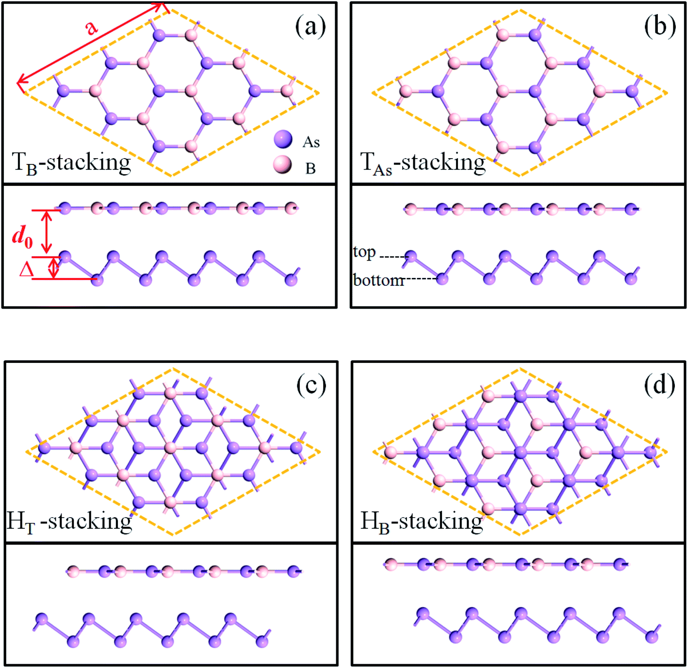 | ||
| Fig. 1 Four stacking structures of BAs/As, where the supercell (3 × 3 × 1) is represented by the diamond frame. (a)–(d) Top and side views of TB-, TAs-, HT-, and HB-stacking. The pink and purple represent B and As atoms, respectively. The interlay distance between BAs and arsenene layer is d0. | ||
In order to find the most stable stacking mode of the BAs/As heterostructure, four stacking structures were geometrically optimized and the corresponding parameters were measured, which are listed in Table 1. The different stacking modes have little effects on the lattice constant (s) of the heterostructure and the buckling height (Δ) of arsenene; the average value is about 10.4 Å and 1.44 Å, respectively.
| Patterns | TB | TAs | HT | HB |
| a (Å) | 10.4089 | 10.3956 | 10.4005 | 10.3963 |
| d0 (Å) | 4.01992 | 4.22762 | 3.98022 | 4.3464 |
| Δ (Å) | 1.43896 | 1.43765 | 1.43832 | 1.43986 |
| Eb (eV) | −3.70844 | −3.50571 | −3.81247 | −3.39489 |
| Eg (eV) | 0.298246 | 0.331807 | 0.254416 | 0.275914 |
The lattice optimized constant of the heterostructure is biased to the BAs layer as the wrinkled arsenene has good flexibility. Binding energy (Eb) is computed to determine the interlayer interaction: Eb = EHS − EBAs − ESnC, where EHS is the total energy of heterostructure, and EBAs and ESnC are the total energies of the isolated BAs and As monolayer, respectively.
The binding energies of TB-, TAs-, HT-, and HB-stacking are −3.70, −3.50, −3.81 and −3.39 eV, respectively, which indicate that the formation of the BAs/As heterostructure is energetically favorable. HT-stacking is the most stable BAs/As stacking structure with the least value, and it has the minimum band gap (Eg) of 0.25 eV and the shortest inter-layer distance (d0) of 3.98 Å in the four configurations. In the following, we choose the HT-stacking BAs/arsenene heterostructure as an example to investigate the strain and electric field regulation.
3. Results and discussion
3.1 Electronic structures
As a comparison, we first calculated the electronic band structures for the BAs and As monolayers, as shown in Fig. 2(a) and (b), respectively. The valence band maximum (VBM) and conduction band minimum (CBM) are at Γ-point, indicating a direct band gap of 0.71 eV for the BAs monolayer. InSe monolayer is a semiconductor with an indirect bandgap of 1.33 eV, where the conduction band minimum (CBM) locates at the Γ point, but the valence band maximum (VBM) locates between M and Γ-point.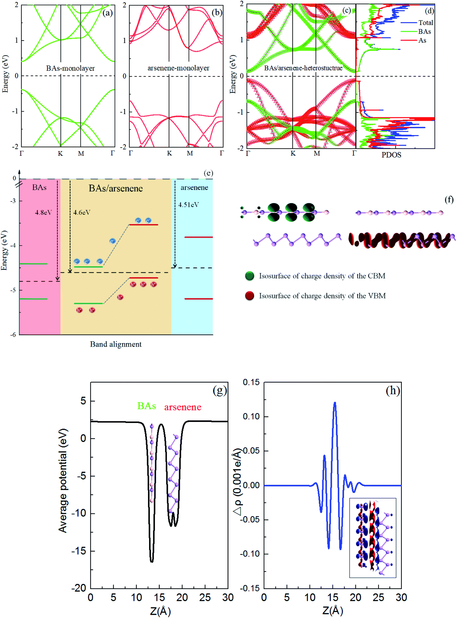 | ||
| Fig. 2 The band structures for (a) BAs and (b) arsenene; (c) and (d) the projected band structure and projected density of states (PDOS) of the BAs/As heterostructure. The subbands contributed by BAs and arsenene are represented by green and red colors, respectively. The Fermi level (EF) is set to zero and indicated by the black dotted line. (e) The band alignment of the heterostructure; (f) isosurface plots of the band decomposed charge densities corresponding to the CBM and the VBM with an isovalue of 0.01 e Å−1; (g) the average electrostatic potential of the heterostructure along the z direction; (h) the plane-averaged charge density difference along the z direction. The inset shows the corresponding isosurface of charge density difference with an isovalue of 0.001 e Å−1, and the red and blue represent electrons gaining and losing, respectively. | ||
The projected band structure of the BAs/As heterostructure is shown in Fig. 2(c). The remarkable changes at VBM and CBM are observed as compared with those of isolated monolayers. The obtained BAs/As heterostructure is also a direct semiconductor with a band gap of 0.25 eV, which is much less than that of a single layer. We can clearly see that the CBM (VBM) of the heterostructure is mainly contributed by the BAs (arsenene) monolayer. The total and partial density of states (PDOS)27–29 are also plotted in Fig. 2(d), along with the decomposed charge density of VBM and CBM in Fig. 2(e). From the calculated PDOS, it can be seen that VBM is dominated by the states from the As layer and the CBM is mainly provided by the states from the BAs layer. The decomposed charge density of the VBM and CBM in Fig. 2(e) also clearly shows that the electrons and holes are mainly localized on the BAs region and As region, respectively, which coincides with the DOS and projected band structure analysis above. Therefore, the full separation of the charge distributions of VBM and CBM will favor the efficient separation of photogenerated electron–hole pairs in the BAs/As heterostructure, which is crucial to the performance of optoelectronic devices.30–32 Furthermore, the band alignment of the BAs/As heterostructure is shown in Fig. 2(f), which also demonstrates the type-II characteristics. Moreover, band offsets are crucial factors in the application of optoelectronic devices. The valence-band offset (VBO) and conduction-band offset (CBO) between the hetero bilayer are 1.19 eV and 0.82 eV in Fig. 2(f), respectively. When the BAs/As heterostructure is irradiated by light, the photogenerated electrons will transition from the valence bands of BAs (arsenene) to the conduction bands, respectively. In addition, the photogenerated electrons in the arsenene layer can be transferred to the conduction band of BAs due to the existence of CBO, while the photogenerated holes can transfer from the valence band of BAs to the arsenene. Therefore, both CBO and VBO can promote the separation of photogenerated electron–hole pairs.33
The work function of As (BAs, heterostructure) is 4.51 eV (4.80 eV, 4.60 eV). Therefore, electrons transfer from As to BAs, and the holes transfer from BAs to arsenene, forming the built-in electric field (Eint) at the interface with the direction of Eint being from As to BAs, which prevents the continuous transferring of charge until dynamic equilibrium. In addition, we also considered the average electrostatic potential of the system. Fig. 2(g) shows that there is a deeper average electrostatic potential well in BAs than arsenene in the heterostructure. The potential difference makes it easier to transfer electrons from the arsenene monolayer to the BAs layer.34
To further clarify the underlying mechanism of the interlayer binding between the BAs/As heterostructure, the integrated charge density difference (Δρ) between the isolated monolayers and heterostructure was investigated. The average charge density difference of the xy plane along the z direction is shown in Fig. 2(h), which is calculated as:
| Δρ(z) = ∫ρhetero(x,y,z)dxdy − ∫ρAs(x,y,z)dxdy − ∫ρBAs(x,y,z)dxdy |
3.2 Electronic structure modified by an external electric field
Applying a vertical external electric field (Eext) to the heterostructure is an effective route to tune the electronic structure, and the calculated results are shown in Fig. 3. The positive direction of Eext is set from As to BAs, as shown in the inset of Fig. 3(a). The electronic structure of the BAs/As heterostructure is considerably changed although the geometrical structure undergoes inconspicuous change under different Eext. In addition, Fig. 3(a) also plots the band gap of the BAs/As heterostructure as a function of the external E-field. The band gap is very sensitive towards electric field regulation. When E-field is positive and less than 0.5 V Å−1, the band gap retains the monotonously decreasing trend and then shows a linear decrease with E-field. When a negative electric field is applied, the bandgap is reduced in a linear way. It is interesting that the BAs/As heterostructure experiences semiconductor to metal transition when the negative external E-field is larger than −0.2 V Å−1, which can lead to tunable transport and conductivity properties.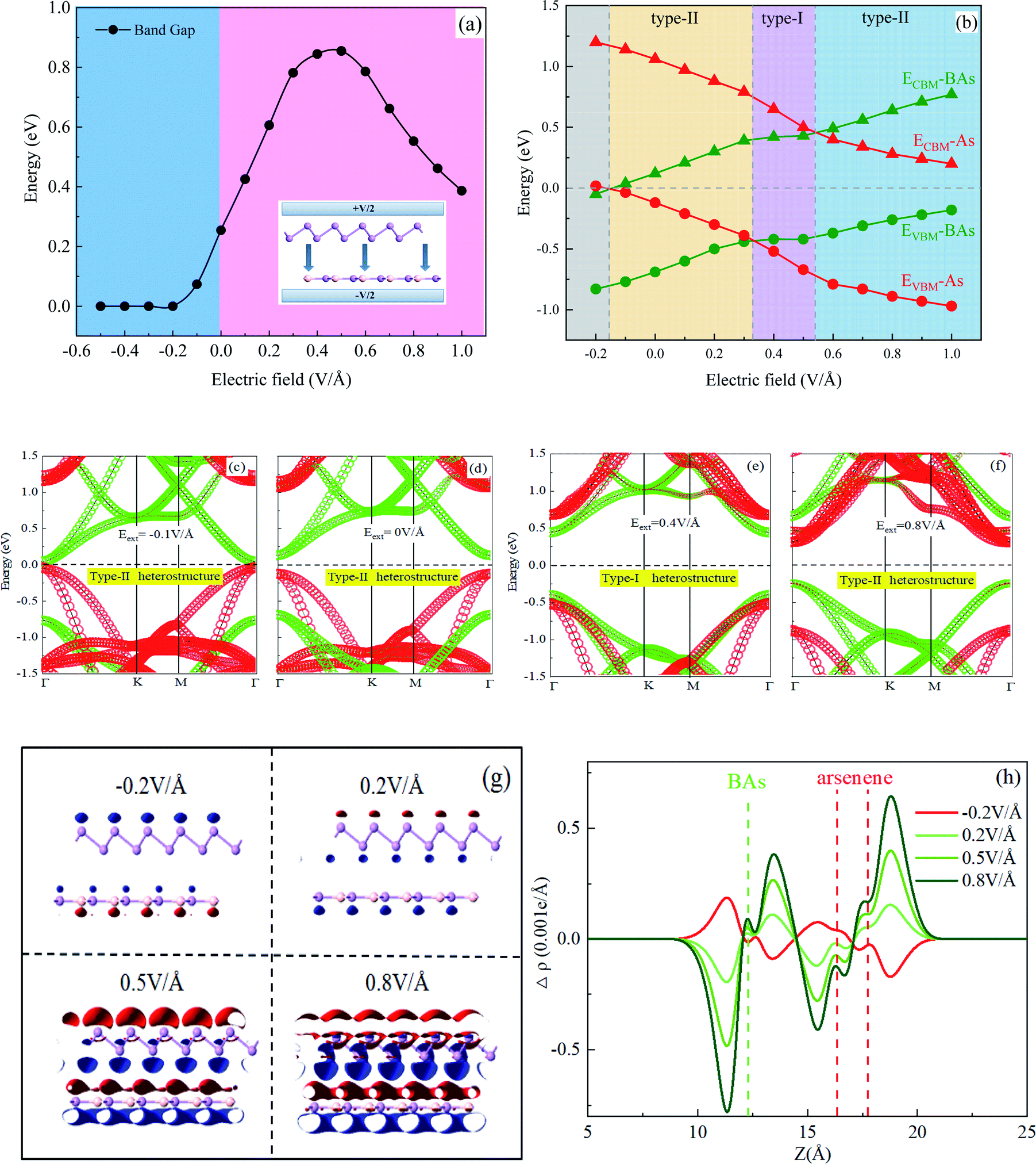 | ||
| Fig. 3 (a) and (b) The calculated band gap and band edge position as a function of E-field for the BAs/As heterostructure, and the inset shows the positive direction of Eext; (c)–(f) the projected band structure of the heterostructure at the E-field of −0.1, 0, 0.4 and 0.8 V Å−1; (g) and (h) the isosurface of integrated charge density difference at the E-field of −0.2, 0.2, 0.5 and 0.8 V Å−1, and the isovalue of the plot is 0.0003 e Å−3. | ||
The changes in the band edges of BAs and arsenene monolayer in the BAs/As heterostructure under electric field regulation are shown in Fig. 3(b). The physical mechanism of applying Eext on the heterostructure is the shift of the band edge, which can be understand by the Stark effect.37 It can be seen that the width of the band gap formed between CBM and VBM for the arsenene (BAs) layer changed slightly under an external E-field. On the other hand, both CBM and VBM of the arsenene layer down-ward shifted in the range of electric field of [−0.2 V Å−1, 1.0 V Å−1], while the BAs layer showed an opposite trend. Therefore, the band alignment type of the BAs/As heterostructure is different under the regulation of electric field due to the opposite trend of CBM and VBM of the two monolayers. Once the Eext exceeds 0.6 V Å−1 or is below 0.3 V Å−1, the type-I heterostructure transforms to type-II with VBM and CBM lying in different monolayers, respectively, resulting in the different spatial distribution of electrons and holes. The BAs/As heterostructure exhibits a type-I behavior with the external E-field of [0.3 V Å−1, 0.5 V Å−1], resulting in both VBM and CBM localized on BAs. For comparison, the variation of projected band structures under the different Eext (−0.1, 0, 0.4 and 0.8 V Å−1) are plotted in Fig. 3(c)–(f). It is found that the band edge of arsenene (the red section) shift downward, while the band edge of BAs (the green section) shifts in the opposite direction under E-field. Therefore, the accumulation of photogenerated electron–hole pairs changes with E-field.
To further explore how external electric field modulates the electric properties of the interlayer binding of the BAs/As heterostructure, the integrated charge density difference is shown in Fig. 3(g) and (h), which is defined as:
| ΔρEext(Z) = ∫ρEext(x,y,z)dxdy − ∫ρE0(x,y,z)dxdy |
3.3 Electronic structure modified by vertical strain
The electronic band structure for the heterostructure can also be easily modified by altering the interlayer spacing distance along the vertical direction, which affects the vdW interaction. In the BAs/As heterostructure, the electronic band structure varied with vertical strain ε investigated, as shown in Fig. 4(a). Here, the vertical strain is defined as ε = d − d0, where d0 = 3.98 Å is the equilibrium interlayer distance. From Fig. 4(a), we can see that the interlayer distance is reduced and the band gap of the heterostructure exhibits a decreasing trend when compressive strain is exerted. On the contrary, a larger interlayer distance is induced and the band gap increases when the stretch strain is applied. In order to understand mechanism of the variation of band gap under vertical strain, the integrated charge density difference is shown in Fig. 4(b)–(d). It can be seen clearly that there is considerable charge accumulation in the middle of the heterostructure with the compressive strain, and the electron transfer from As to BAs. The charge redistribution led to the polarization of electron and formation of interface dipole, causing surface orbital rehybridization. The smaller interlayer distance leads to a stronger interaction between BAs and As, which causes more charges transfer. Thus, a higher built-in E-field can be obtained, which will reduce the band gap of the heterostructure.40 Conversely, the transferring electrons reduce in the intermediate position of BAs/As when applying a stretch strain.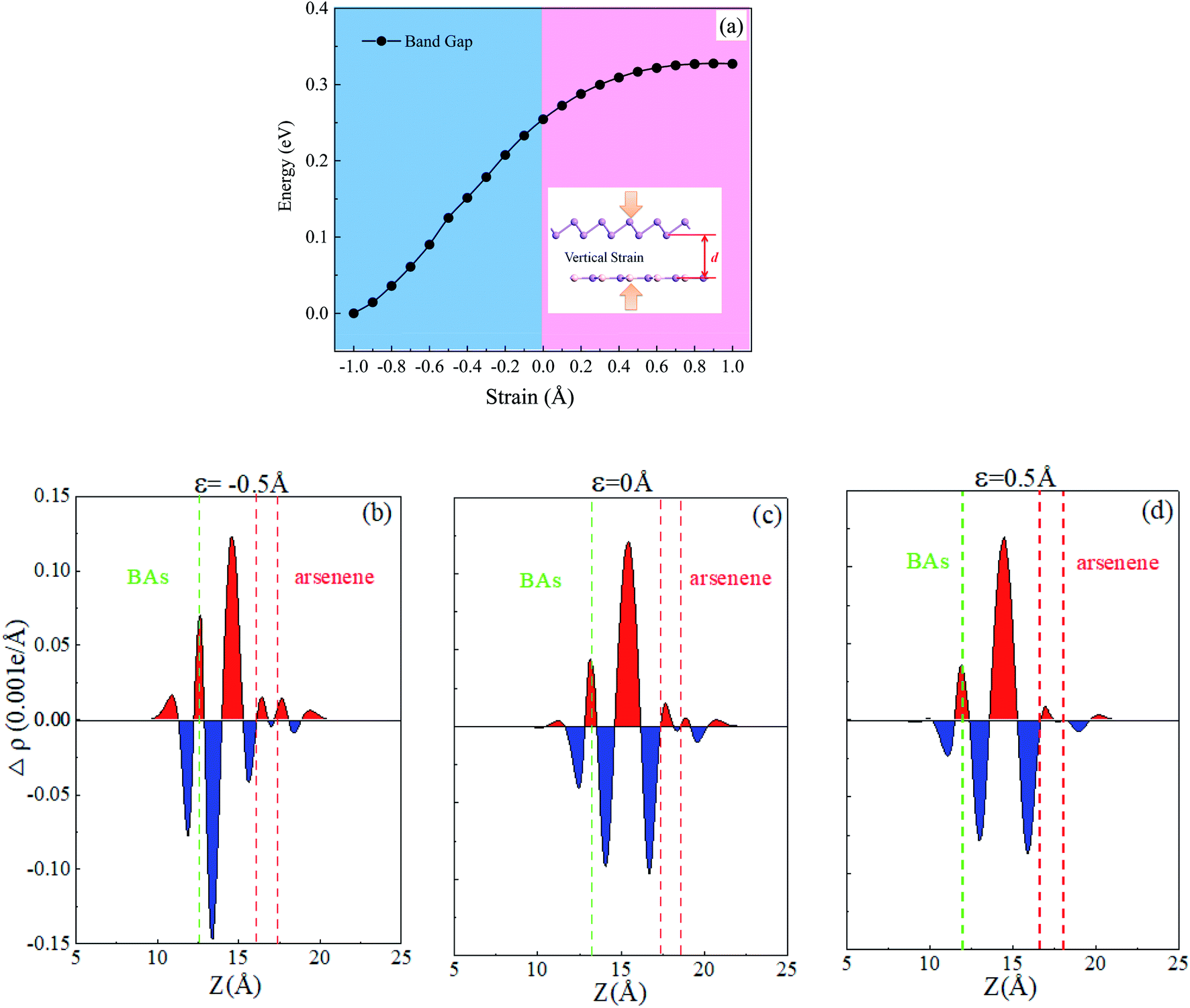 | ||
| Fig. 4 (a) The calculated band gap and band edge position as a function of the vertical strain for the BAs/As heterostructure; (b–d) the plane-averaged charge density difference of the heterostructure under the selected vertical strain (ε = −0.5, 0, 0.5 Å). The green and red vertical dash lines indicate the position of BAs and arsenene layer in the heterostructure. | ||
3.4 Optical properties
Now, we investigated the optical properties of the BAs/As heterostructure under vertical strain and external electric field. The optical absorption coefficient α(ω) was evaluated via density functional theory calculations. There is the weak chemical bonding crossing the vdW gap, and the nature of weak interactions is decisive for numerous extraordinary properties.36where ε1(ω) and ε2(ω) are the real and imaginary parts of frequency-dependent dielectric function, respectively. We calculated the light absorption of the BAs/As heterostructure, isolated BAs and arsenene monolayer in X, Y and Z directions, respectively, as shown in Fig. 5(a). The results show that the absorption peak value of the Z direction is obviously lower than that of X and Y directions. Due to the overlap of the electronic states, the BAs/As heterostructure has a wider absorption range and stronger absorption capacity for visible light compared with the isolated monolayer, which is expected to be applied in solar cells. One possible route to tune the optical absorption characteristics of the heterostructure is to apply a vertical external electric field, as shown in Fig. 5(b): it can be seen that the absorption peak in the Z direction of the BAs/As heterostructure increases with the positive Eext and shows blue-shift towards visible light region, and the absorption range covers the visible region. On the contrary, the absorption spectrum shows red-shift with negative Eext. In addition, interlayer coupling that originates from the different interlayer distances with the vertical strain also affects the optical absorption characteristics, as shown in Fig. 5(c). It can be seen that the absorption peak of heterojunction becomes higher by compression, and the absorption range also changes, leading to blue-shift of the absorption edge, while stretching shows the opposite property. Therefore, the effective modulation of optical absorption characteristics by interlayer coupling or external electric field suggests great potential applications of the BAs/As heterostructure in photodetector devices.
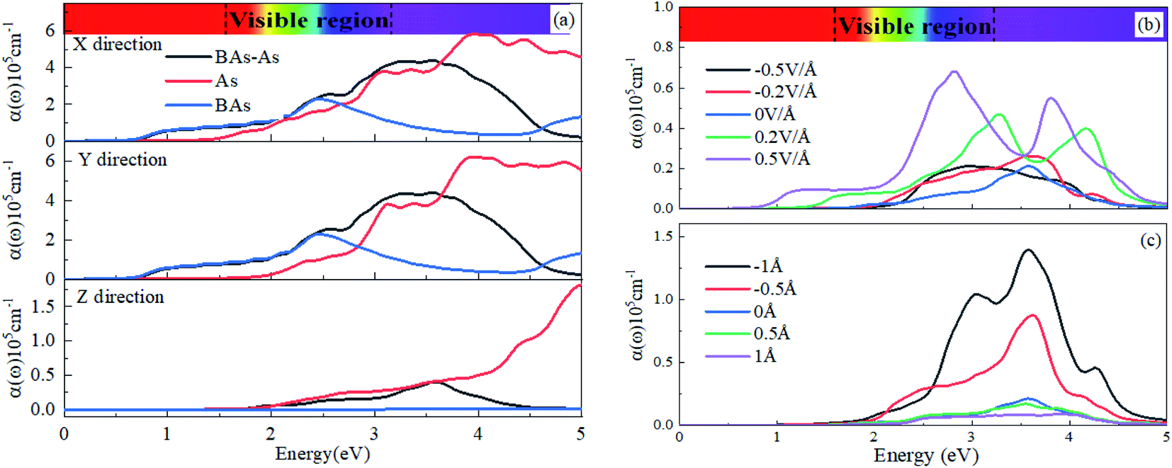 | ||
| Fig. 5 Optical absorption spectra of the heterostructure and monolayers for incident light polarization (a) parallel and perpendicular to the surface. Optical absorption spectra of the heterostructure with different (b) E-field and (c) vertical strain for incident light polarization perpendicular to the surface. | ||
4. Conclusions
We investigated the electronic and optical properties of the BAs/As vdW heterostructure via the density functional theory, and found that these properties can be effectively tuned by applying vertical strain and external electric field. The BAs/As vdW heterostructure exhibited a type-II band alignment with a direct band gap of 0.25 eV, which is good for the separation of photogenerated electron–hole pairs. The energy band varied linearly by vertical strain, and experienced direct–indirect-zero band gap transition. The semiconductor-to-metal transition could be obtained by applying strong electric field. The absorption strength could be tuned mainly by the interlayer coupling, while external electric field showed obvious regulating effects on the absorption strength and absorption edge. The designed vdW heterostructure exhibited a wide absorption range and is expected to have great potential applications in nano-electronic devices and photovoltaics.Conflicts of interest
There are no conflicts to declare.Acknowledgements
This work was supported by the National Natural Science Foundation of China (Grant No. 61771076 and 51604042), and the Scientific Research Fund of Hunan Provincial Education Department (Grant No. 18A140, 18B157 and 17C0031), and the Open Research Fund of Human Provincial Key Laboratory of Flexible Electronic Materials Genome Engineering (Grant No. 202008 and 202013).References
- L. Duan, J. Qiao, Y. Sun and Y. Qiu, Adv. Mater., 2011, 23(9), 1137 CrossRef CAS PubMed.
- C. Zhang, Y. Lu, Z. Liu, Y. Zhang, L. Wang, D. Zhang and L. Duan, Adv. Mater., 2020, 32(42), 2004040 CrossRef CAS PubMed.
- X. Q. Deng, Z. H. Zhang, G. P. Tang, Z. Q. Fan, L. Sun and C. X. Li, Org. Electron., 2016, 35, 1 CrossRef CAS.
- B. M. Duggan, R. Cullum, W. Fenical, L. A. Amador, A. D. Rodríguez and J. Clair, Angew. Chem., Int. Ed., 2020, 132(13), 5025 CrossRef.
- B. Anasori, M. R. Lukatskaya and Y. Gogotsi, Nat. Rev. Mater., 2017, 2(2), 16098 CrossRef CAS.
- Z. Q. Fan, Z. H. Zhang and S. Y. Yang, Nanoscale, 2020, 12(42), 21750 RSC.
- Z. Song, Z. Li, H. Wang, X. Bai, W. Wang, H. Du, S. Liu and C. Wang, Nano Lett., 2017, 17(3), 2079 CrossRef CAS PubMed.
- J. Wang, F. Ma and M. Sun, RSC Adv., 2017, 7, 16801 RSC.
- X. Wang and F. Xia, Nat. Mater., 2015, 14(3), 264 CrossRef CAS PubMed.
- L. Huang and J. Li, Appl. Phys. Lett., 2016, 108(8), 083101 CrossRef.
- J. K. Hu, J. X. Tan, D. Wu, Z. H. Zhang and Z. Q. Fan, Appl. Surf. Sci., 2021, 560, 149858 CrossRef CAS.
- W. Yu, Z. Zhu, S. Zhang, X. Cai, X. Wang, C. Y. Niu and W. B. Zhang, Appl. Phys. Lett., 2016, 109(10), 103104 CrossRef.
- H. Zeng, J. Zhao, A. Q. Cheng, L. Zhang, Z. He and R. S. Chen, Nanotechnology, 2018, 29(7), 075201 CrossRef PubMed.
- X. Wang and F. Xia, Nat. Mater., 2015, 14(3), 264 CrossRef CAS PubMed.
- K. F. Mak and J. Shan, Nat. Photonics, 2016, 10(4), 216 CrossRef CAS.
- D. A. Broido, L. Lindsay and T. L. Reinecke, Phys. Rev. B: Condens. Matter Mater. Phys., 2013, 88(21), 214303 CrossRef.
- R. Zhang, C. Zhang, W. Ji, S. Li, P. Wang, S. Hu and S. Yan, Appl. Phys. Express, 2015, 8(11), 113001 CrossRef.
- S. Ullah, P. A. Denis and F. Sato, ACS Omega, 2018, 3(12), 16416–16423 CrossRef CAS PubMed.
- S. Ullaha, P. A. Denisb and F. Sato, Comput. Mater. Sci., 2019, 170, 109186 CrossRef.
- R. Q. Sheng, X. Q. Deng, Z. H. Zhang and Z. Q. Fan, Phys. Lett. A, 2020, 384(7), 126150 CrossRef CAS.
- S. Ullah, P. A. Denis, M. G. Menezes and F. Sato, Appl. Surf. Sci., 2019, 493, 308–319 CrossRef CAS.
- Z. Q. Fan, X. W. Jiang, J. Chen and J. W. Luo, ACS Appl. Mater. Interfaces, 2018, 10(22), 19271 CrossRef CAS PubMed.
- Z. Q. Fan, X. W. Jiang, J. W. Luo, L. Y. Jiao, R. Huang, S. S. Li and L. W. Wang, Phys. Rev. B, 2017, 96(16), 165402 CrossRef.
- Q. X. Dong, R. Hu, Z. Q. Fan and Z. H. Zhang, Carbon, 2018, 130, 206 CrossRef CAS.
- S. Grimme, J. Comput. Chem., 2004, 25(12), 1463 CrossRef CAS PubMed.
- S. Grimme, J. Antony, S. Ehrlich and H. Krieg, J. Chem. Phys., 2010, 132(15), 154104 CrossRef PubMed.
- H. Şahin, S. Cahangirov, M. Topsakal, E. Bekaroglu, E. Akturk, R. T. Senger and S. Ciraci, Phys. Rev. B: Condens. Matter Mater. Phys., 2009, 80(15), 155453 CrossRef.
- G. Graziano, J. Klimeš, F. Fernandez-Alonso and A. Michaelides, J. Phys.: Condens. Matter, 2012, 24(42), 424216 CrossRef PubMed.
- D. Wang, D. X. Han, L. Liu and L. Niu, RSC Adv., 2016, 6(34), 28484 RSC.
- A. K. Geim and I. V. Grigorieva, Nature, 2013, 499(7459), 419 CrossRef CAS PubMed.
- P. Ajayan, P. Kim and K. Banerjee, Phys. Today, 2016, 69(9), 38 CrossRef CAS.
- Y. Liu, N. O. Weiss, X. Duan, H. C. Cheng, Y. Huang and X. Duan, Nat. Rev. Mater., 2016, 1(9), 16042 CrossRef CAS.
- Z. Guan, C. S. Lian, S. Hu, S. Ni, J. Li and W. Duan, J. Phys. Chem. C, 2017, 121(6), 3654 CrossRef CAS.
- D. Wang, D. X. Han, L. Liu and L. Niu, RSC Adv., 2016, 6(34), 28484 RSC.
- D. S. Koda, F. Bechstedt, M. Marques and L. K. Teles, Phys. Rev. B, 2018, 97(16), 165402 CrossRef CAS.
- H. Kasai, K. Tolborg, M. Sist, J. Zhang, V. R. Hathwar, M. Filsø, S. Cenedese, K. Sugimoto, J. Overgaard, E. Nishibori and B. Iversen, Nat. Mater., 2018, 17(3), 249 CrossRef CAS PubMed.
- L. Huang and J. Li, Appl. Phys. Lett., 2016, 108(8), 083101 CrossRef.
- W. Li, T. Wang, X. Dai, Y. Ma and Y. Tang, J. Alloys Compd., 2017, 705, 486 CrossRef CAS.
- X. C. Ma, Y. Dai, L. Yu and B. B. Huang, Light: Sci. Appl., 2016, 5(2), 16017 CrossRef PubMed.
- C. Xia, J. Du, W. Xiong, Y. Jia, Z. Wei and J. Li, J. Mater. Chem. A, 2017, 5(26), 13400 RSC.
| This journal is © The Royal Society of Chemistry 2021 |