
 Open Access Article
 This Open Access Article is licensed under a Creative Commons Attribution-Non Commercial 3.0 Unported Licence
The impact of fluence dependent 120 MeV Ag swift heavy ion irradiation on the changes in structural, electronic, and optical properties of AgInSe2 nano-crystalline thin films for optoelectronic applications
R. Panda *a,
S. A. Khanb,
U. P. Singhc,
R. Naik*d and
N. C. Mishraae
*a,
S. A. Khanb,
U. P. Singhc,
R. Naik*d and
N. C. Mishraae
aDepartment of Physics, Utkal University, Bhubaneswar 751008, India
bInter-University Accelerator Centre, New Delhi, 110 067, India
cKIIT University, Bhubaneswar, 751024, India
dDepartment of Material Engineering and Physics, ICT-IOC, Bhubaneswar 751013, India
eDepartment of Physics, U.N. College of Sc. and Tech., Adaspur 754011, India
First published on 30th July 2021
Abstract
Swift heavy ion (SHI) irradiation in thin films significantly modifies the structure and related properties in a controlled manner. In the present study, the 120 MeV Ag ion irradiation on AgInSe2 nanoparticle thin films prepared by the thermal evaporation method and the induced modifications in the structure and other properties are being discussed. The ion irradiation led to the suppression of GIXRD and Raman peaks with increasing ion fluence, which indicated amorphization of the AgInSe2 structure along the path of 120 MeV Ag ions. The Poisson's fitting of the ion fluence dependence of the normalized area under the GIXRD peak of AgInSe2 gave the radius of the ion track as 5.8 nm. Microstructural analysis using FESEM revealed a broad bi-modal distribution of particles with mean particle sizes of 67.5 nm and 159 nm in the pristine film. The ion irradiation led to the development of uniform particles on the film surface with a mean size of 36 nm at high ion fluences. The composition of the film was checked by the energy dispersive X-ray fluorescence (EDXRF) spectrometer. The UV-visible spectroscopy revealed the increase of the electronic bandgap of AgInSe2 films with an increase in ion fluence due to quantum confinement. The Hall measurement and EDXRF studies showed that the unirradiated and irradiated AgInSe2 films have n-type conductivity and vary with the ion fluence. The changes in the films were tuned with different ion fluence and are favorable for both optical and electronic applications.
1. Introduction
The response of materials to intense excitation, such as high temperature, high pressure, or particle irradiation, is of considerable interest both for fundamental studies and technological applications. These excitations can modify the structure and many other properties of the material, which can provide new functionalities and hence make the material useful for many applications. Among the different post-deposition excitations employed for modifications of materials in thin films, irradiation by energetic ions with energies more than 1 MeV amu is unique owing to its capability to instantaneously deposit very high energy density in a highly localized columnar region of a few nm radius and a few tens of micrometer length along the ion path in the material.Present accelerators can deliver particles with an energy ranging from a few keV to several hundreds of GeV, and depending upon the energy imparted to the materials, ion beams obtained from these accelerators are classified into two types. The low-energy ion beams have an energy ranging from a few keV to a few hundreds of keV, which lose energy in their passage through elastic collisions with the atoms of the material. The second type of ion irradiation is the swift heavy ions (SHI), which are positively charged ions with large atomic mass and hundreds of MeV energy. When these ions pass through the material medium, they interact with electrons and with nuclei, possibly also with the medium as a whole. Generally, the interaction of SHI with matter results in the transfer of energy of the incident ions to the electrons since the velocity of the ions can be – Bohr velocity of electrons. The ions thereby modify the structural, electrical, optical, optoelectronic, transport, and many other properties of the materials.1 The SHI traversing through a material loses energy mainly through two nearly independent processes: (i) elastic collisions with the target nuclei and (ii) electronic excitation and ionization of the target atoms.2 The first process is called the nuclear energy loss,  , which dominates at low ion energies (keV amu−1) and leads to atomic displacements through direct elastic knock-on process.3–5 The second process is called the electronic energy loss,
  that prevails for SHI and creates significant atomic rearrangements in various types of materials by transferring energy from the excited electrons to the lattice atoms along the path of the ions.6–9 In the case of crystalline materials, when the value of Se exceeds a threshold value, Seth i.e., Se > Seth, the electronic energy loss process leads to the formation of an amorphous latent track along the ion trajectory. The Seth is material dependent, and if Se is less than Seth, some additional defects may appear, and sometimes the pre-existing defects may anneal out.10,11
From previous studies, Ag ions are mostly used for irradiation to obtain significant results, which are beneficial for many fields including antibacterial application and photo-catalytic performance, photonic crystals, surface coatings, and enhancing solar cell efficiency.12,13 Hence, we have preferred Ag ion instead of other ions for implantation as silver diffuses easily into chalcogenide materials.
One of the prominent members of the I–III–VI chalcogenide family of semiconductors is AgInSe2, which has found extensive applications in many areas like photovoltaics,14 preparation of Schottky diodes,15 optoelectronic device as hetero-junction,16 non-linear optical devices,17 light emitting and detecting devices,18 solar cell absorbing material,19 etc. Most of the applications of this material are realized in its thin film form. The material modification by various external energy sources like laser irradiation,20 thermal annealing,21 γ irradiation,22 proton irradiation,23 etc. brings significant changes in their optical as well as structural properties. Though SHI irradiation has been extensively used for the modification of thin films of a variety of materials, only a few studies have been undertaken on SHI induced effects in AgInSe2 films.24–26 In one study, Pathak et al. reported the formation of AgInSe2 nanorods under 200 MeV Ag ion irradiation at a fluence of 5 × 10¹¹ ions per cm2.24 In another study, the same authors reported unexpected complete damage of the chalcopyrite structure of AgInSe2 at extremely low ion fluences (5 × 10¹⁰ ions per cm2).25 In the present study, we have tried to observe the modification by 120 MeV Ag ion at fluences (i) 1 × 10¹¹ ions per cm2, (ii) 1 × 10¹² ions per cm2 and (iii) 1 × 10¹³ ions per cm2 in which two fluences are higher in order. We have reported that each 140 MeV Ni ion traversing the AgInSe2 medium creates two structural modifications: (i) an amorphous column of 1.6 nm radius along the ion path and (ii) a radially compressed crystalline column of 8.2 nm radius surrounding the amorphous column.26 However, the optical and electronic modification due to structural change by the SHI irradiation at different fluences is not investigated in AgInSe2 films.
In the present work, we have examined the 120 MeV Ag ion irradiation-induced modifications on the structural, electrical, and optical properties of AgInSe2 nano-crystalline thin films grown on glass substrates by the thermal evaporation method. The irradiation was done at three different fluences in order to investigate the fluence dependent change in the properties. The structural transformation was studied through grazing incidence X-ray diffraction (GIXRD) and Raman spectroscopy. The morphological change was analyzed by field emission scanning electron microscopy (FESEM). The compositional check was carried out by Energy Dispersive X-ray Fluorescence (EDXRF) spectrometer. The optical study was done by the UV-visible spectrometer that revealed the increase in the optical bandgap. We also demonstrated that the particles on the surface of the pristine films with wide distribution in their size develop into uniform size particles of much smaller size in the irradiated films with an associated increase of bandgap due to quantum confinement. The Hall measurement study was done to measure the conductivity of the films.
2. Experimental procedure
Thin films of AgInSe2 were deposited on glass substrates by the thermal evaporation method from the bulk target. The bulk synthesis involved the melt quenching of a mixture of highly pure Ag (99.99%), In (99.9%), and Se (99.95%) powders in stoichiometric proportions (1![[thin space (1/6-em)]](https://www.rsc.org/images/entities/char_2009.gif) :1:2) taken in a quartz ampoule, which was evacuated at a pressure of 10−5 torr and sealed. The temperature of the quartz ampoule placed in a furnace was slowly raised to 1000 °C and maintained at that temperature for 36 h with continuous rotational shaking of the ampoule to ensure homogeneous mixing of the different constituent elements in it. The powder in the ampoule melted as the furnace temperature was higher than the melting temperature of AgInSe2 780 °C. The melt was then quenched by dropping the ampoule in ice-cooled water to obtain the target in the form of an ingot for thin film preparation. Thin films of AgInSe2 were deposited on a glass substrate by the thermal evaporation method using a Hind High vacuum coating unit (Model-12A4D). The substrate was initially cleaned with a detergent solution and then ultrasonically cleaned with distilled water and acetone. The AgInSe2 ingot was placed in a molybdenum boat kept about 15 cm below the substrate in a vacuum of ∼1 × 10⁻⁵ torr. The deposition was done at room temperature. The films thus developed had a thickness of ∼0.6 μm as measured by the quartz crystal monitor attached inside the coating unit. The as-prepared films were annealed at 200 °C for 1 h in a selenium atmosphere.
:1:2) taken in a quartz ampoule, which was evacuated at a pressure of 10−5 torr and sealed. The temperature of the quartz ampoule placed in a furnace was slowly raised to 1000 °C and maintained at that temperature for 36 h with continuous rotational shaking of the ampoule to ensure homogeneous mixing of the different constituent elements in it. The powder in the ampoule melted as the furnace temperature was higher than the melting temperature of AgInSe2 780 °C. The melt was then quenched by dropping the ampoule in ice-cooled water to obtain the target in the form of an ingot for thin film preparation. Thin films of AgInSe2 were deposited on a glass substrate by the thermal evaporation method using a Hind High vacuum coating unit (Model-12A4D). The substrate was initially cleaned with a detergent solution and then ultrasonically cleaned with distilled water and acetone. The AgInSe2 ingot was placed in a molybdenum boat kept about 15 cm below the substrate in a vacuum of ∼1 × 10⁻⁵ torr. The deposition was done at room temperature. The films thus developed had a thickness of ∼0.6 μm as measured by the quartz crystal monitor attached inside the coating unit. The as-prepared films were annealed at 200 °C for 1 h in a selenium atmosphere.
The annealed films were irradiated by 120 MeV Ag ions using the 15 UD tandem Pelletron accelerator at IUAC, New Delhi. The ions bombarded the sample surface perpendicularly. For uniform irradiation, an ion beam was made to scan 1 cm × 1 cm area of the sample surface. To prevent sample heating, a thick copper ladder was used to mount the samples using silver paste and a low ion flux, φ (∼1 × 10⁹ ions per cm2 per S1) was maintained. At this flux, the increase in temperature on the sample surface during irradiation as estimated using Fourier heat conduction equation27 was found to be below 5 K. Thus, the beam heating effect can be ruled out to account for the observed modifications induced by ion beams. During irradiation, the target ladder was placed inside a high vacuum chamber (10−6 torr). The irradiation was done at three different fluences 1 × 10¹¹, 1 × 10¹², and 1 × 10¹³ ions per cm2.
Structural characterization of the pristine and the irradiated films was carried out in GIXRD mode of a Bruker D8 advanced X-ray diffractometer with Cu Kα (λ = 1.5401 Å) radiation source. The incident angle of X-rays was kept at 2° with respect to the sample surface. GIXRD patterns were recorded over the range of 2θ from 20° to 55° in steps of 0.02° at a scan speed 1° per minute. The transmittance spectra were recorded using a UV-vis spectrophotometer (Bruker IFS 66v/S). Raman spectra of the films were taken using a HORIBA T64000 Raman spectrometer with 514 nm radiation from a 10 mW argon ion laser at room temperature. The microstructural and compositional characterizations were done using the FESEM microscope (ZEISS SIGMA-40 microscope) and EDXRF spectrometer (SHIMADZU-7000), respectively. The electrical study was done by Hall measurement using Ecopia HMS-3000 Hall measurement system.
3. Results and discussion
3.1. Energy loss of 120 MeV Ag ions in AgInSe2 medium
To analyze the evolution of the AgInSe2 phase with 120 MeV Ag ion fluence, we have computed the irradiation parameters Sn, Se, and range R of 120 MeV Ag ions in AgInSe2 and glass substrate using SRIM code.28 Fig. 1 gives the variation of the Sn and Se with depth as the 120 MeV Ag ions penetrate first into the AgInSe2 thin film and then the glass substrate. The ions lose energy along their path in the film, and the substrate finally gets implanted at a depth of about 14.2 μm in the film. Fig. 1 also shows that Se dominates up to a depth of 12 μm, beyond which Sn increases and peaks at the end of the range before the projectile ions get implanted in the glass substrate. Since the implantation occurs far beneath the surface of the substrate, the implanted ions do not contribute to the modifications induced in the film. Further, the Se is about 180 times larger than the Sn in the film. Therefore, the modifications induced into the AgInSe2 films is primarily due to the Se of 120 MeV Ag ions. The Se shows only a small decrease from 16.5 keV nm−1 to 16 keV nm−1 as the ions traverse the thickness (0.6 μm) of the AgInSe2 thin films and then a sudden decrease to 13.7 keV nm−1 as these enter the glass substrate. The Se induced modification in the film is thus uniform along the path of the projectile ions.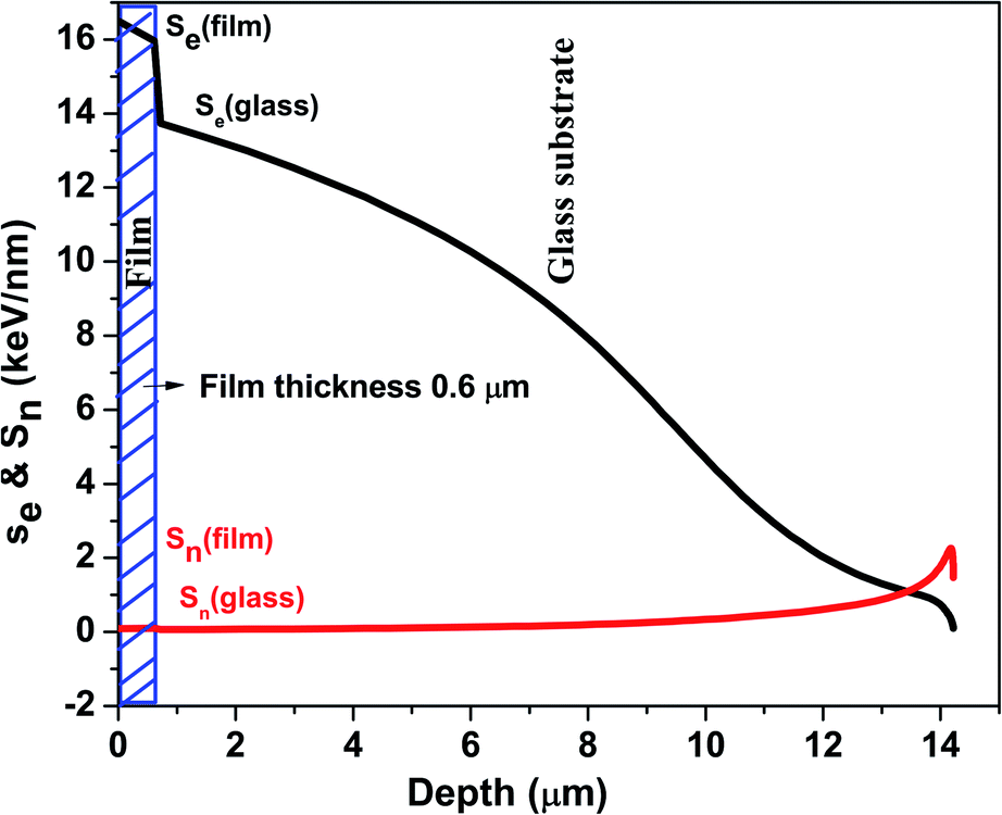 | ||
| Fig. 1 Variation of the electronic energy loss Se and the nuclear energy loss Sn of 120 MeV Ag ions with depth as the ions traverse the thickness of the AgInSe2 thin films. | ||
3.2. Compositional analysis of AgInSe2 thin films by EDXRF
The EDXRF spectrum (Fig. 2) of AgInSe2 thin films revealed the presence of selenium, silver, and indium by their characteristic Kα peaks at 11.20 keV, 22.10 keV, and 24.14 keV, respectively. Analysis of the EDXRF spectra gave the concentration of these elements in the ingot as well as in the films made out of it by thermal evaporation and then irradiated by 120 MeV Ag ions at different fluences (Table 1).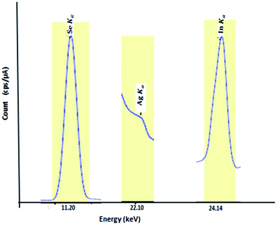 | ||
| Fig. 2 The line scans of Se Kα, Ag Kα, and In Kα in the EDXRF spectrum of pristine AgInSe2 thin film. | ||
| Sample | Ag (atomic %) | In (atomic %) | Se (atomic %) | Off-stoichiometry parameter Δy |
|---|---|---|---|---|
| Ingot | 24.4 | 25.2 | 50.4 | 0.008 |
| Annealed AgInSe2 | 7.686 | 38.112 | 54.202 | −0.112 |
| 1 × 10¹¹ ions per cm2 | 9.504 | 36.364 | 54.132 | −0.087 |
| 1 × 10¹² ions per cm2 | 10.604 | 34.246 | 55.150 | −0.027 |
| 1 × 10¹³ ions per cm2 | 8.408 | 37.008 | 54.584 | −0.086 |
The ingot had a stoichiometric composition of Ag, In, and Se in the ratio ∼1:1:2 corresponding to the AgInSe2 phase. However, the films, both pristine and the irradiated ones, showed the off-stoichiometric composition of these elements (Table 1) with very low Ag concentration compared to the concentration of In and Se. The off-stoichiometry is not much affected by 120 MeV Ag ion irradiation. The defect chemistry model of ternary compounds29 gives the off-stoichiometry parameter Δy (= [2Se/(Ag + 3In)] − 1) for the different samples (Table 1). The parameter Δy is related to the electronic defects. For the films with p-type conductivity, Δy > 0 and that with n-type conductivity, Δy < 0. The negative Δy in all our films indicates that these are n-type, as was confirmed by the Hall measurement discussed later.
3.3. Structural analysis of AgInSe2 thin films irradiated by 120 MeV Ag ions
The XRD spectrum of the AgInSe2 ingot, the films made out of the ingot, and that annealed and irradiated by 120 MeV Ag ions at different fluences are shown in Fig. 3a. The position and relative intensity of all the peaks of the XRD spectrum of the ingot (Fig. 3a(i)) match with that of the polycrystalline AgInSe2 powder reported in the ICDD file (card no. 35-1099). The film deposited by thermal evaporation technique using this ingot as the target did not show any GIXRD peak, which indicated its amorphous structure (Fig. 3a(ii)). Earlier observations have also confirmed the amorphous nature of the as-deposited AgInSe2 films.30 Annealing at 200 °C for 1 h in selenium atmosphere led to the development of a peak at 2θ = 25.51° (Fig. 3a(iii)), which corresponds to the (112) peak of AgInSe2. Annealing at a very low temperature of 200 °C formed the nano-crystalline AIS phase. However, annealing at a higher temperature (250 °C) formed all the peaks of AIS like Ag2Se (002, 120, 102, 121, 013) and AgInSe2 (112), as reported in our earlier paper,31 but the method of preparation was different (DC magnetron sputtering). So, the Ag2Se peak not being present in the current sample might be due to the preparation method (thermal evaporation) and low annealing temperature (200 °C). In the present study, we have taken this annealed film as a reference to compare its GIXRD spectrum with that of the films irradiated by 120 MeV Ag ions at different fluences (Fig. 3a(iv–vi)).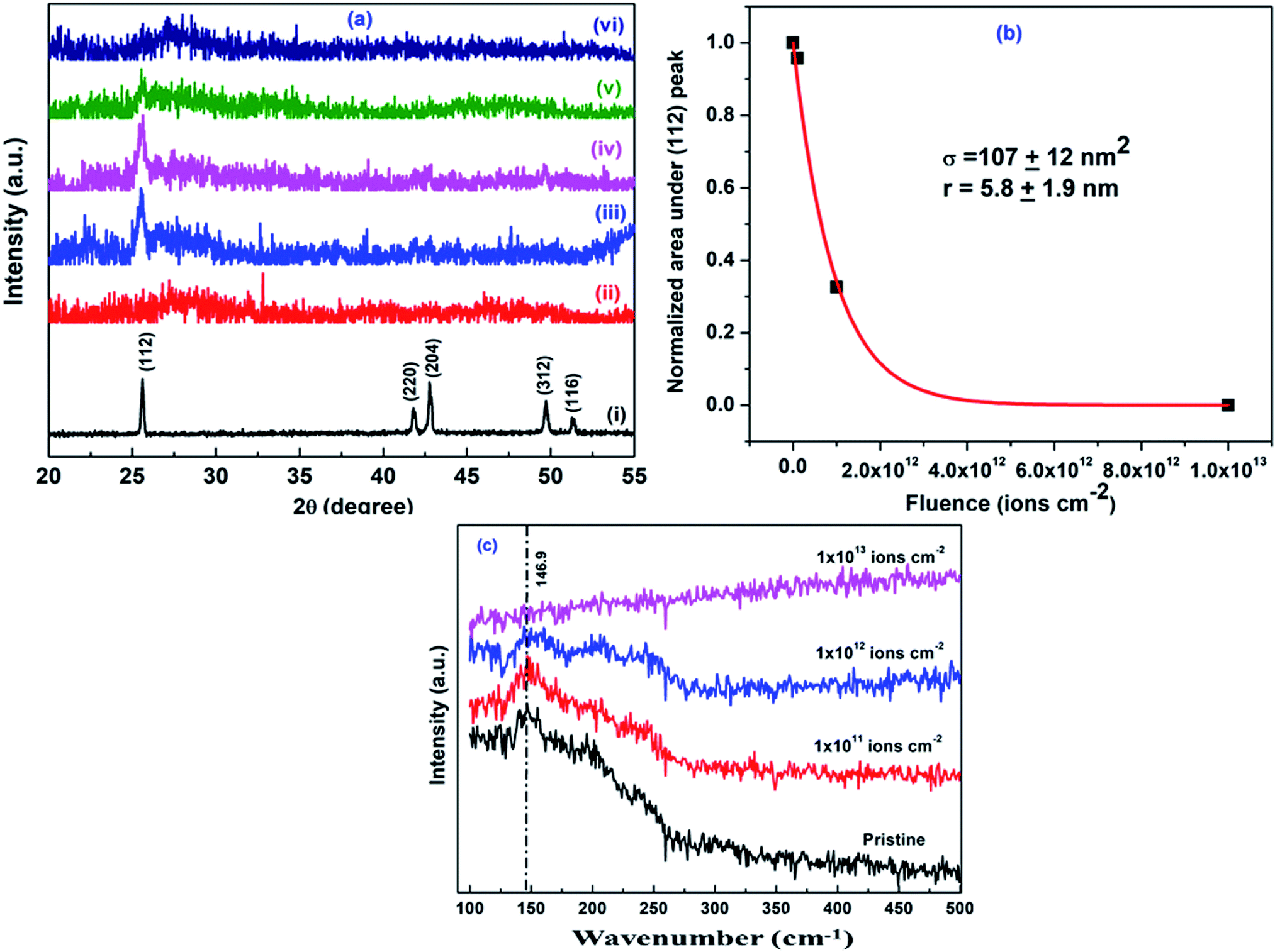 | ||
| Fig. 3 . (a) GIXRD spectrum of (i) AgInSe2 ingot, (ii) as-deposited film made out of the ingot, (iii) the film annealed at 200 °C for 1 h before irradiation and 120 MeV Ag ion irradiated films at fluences (iv) 1 × 10¹¹ ions per cm2, (v) 1 × 10¹² ions per cm2, and (vi) 1 × 10¹³ ions per cm2. (b) Fluence dependent normalized area under the (112) peak of AgInSe2 thin films (c) Raman spectra of pristine and irradiated AgInSe2 thin films. | ||
Irradiation of AgInSe2 films by 120 MeV Ag ions led to suppression of the intensity of its (112) peak with increasing ion fluence. The peak went below the noise level at the fluence of 1 × 10¹³ ions per cm2. Suppression of the GIXRD peak with increasing ion fluence indicates 120 MeV Ag ion irradiation-induced damage in the structure of the AgInSe2 thin film, while the peak disappearing at high ion fluences indicates amorphous track formation along the ion path.32–34 Though the value of Seth for the creation of amorphized latent tracks in AgInSe2 is not known as yet, our observation revealed its value to be less than the Se (16.5 keV nm−1) of 120 MeV Ag ions, which completely amorphized this compound at high ion fluences. To extract the radius of ion tracks, we have fitted the fluence versus normalized area under the (112) GIXRD peak to Poisson equation
| A(φt) = A∞ + (1 − A∞)e−σφt | (1) |
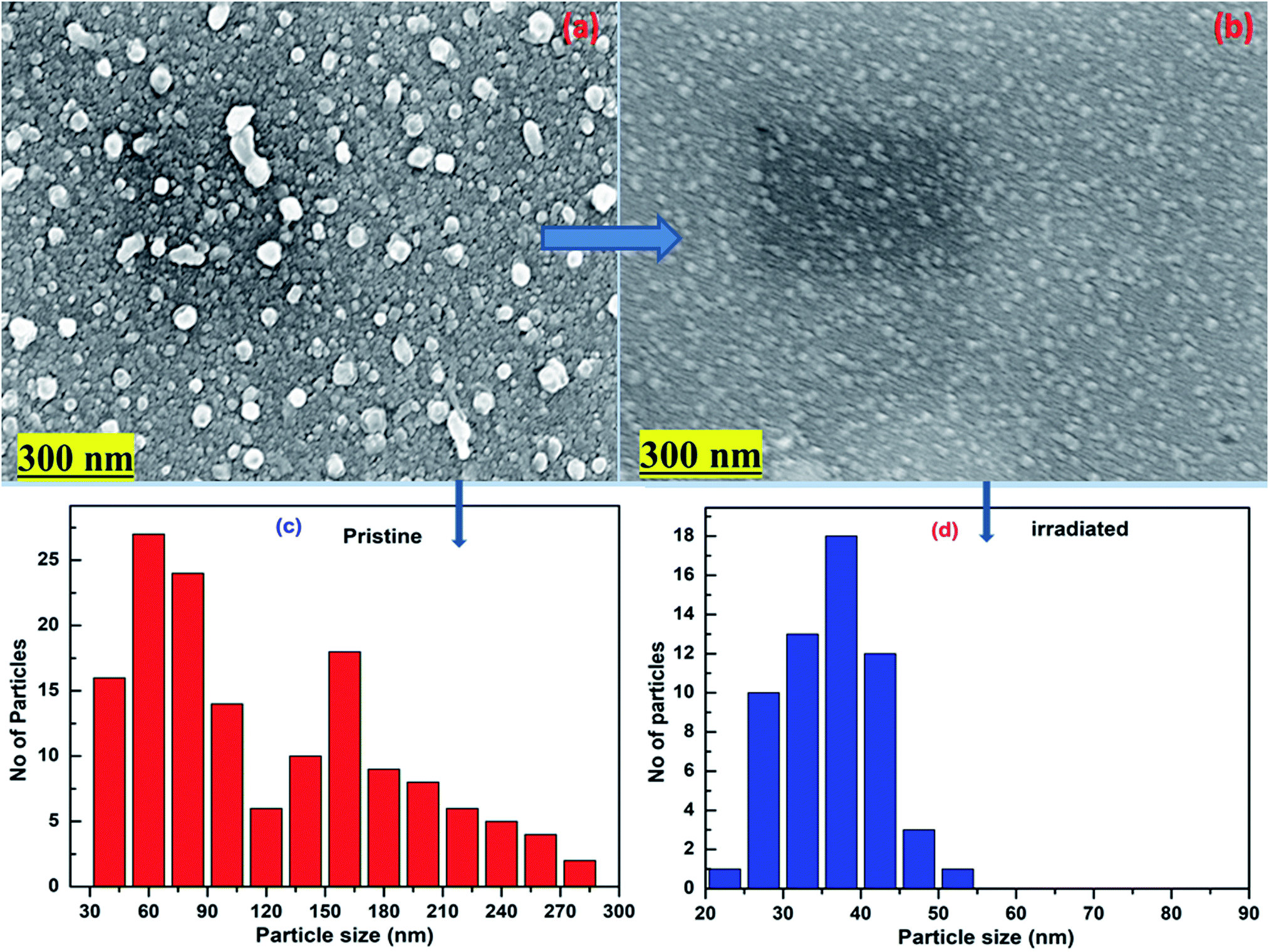 | ||
| Fig. 4 FESEM images of (a) pristine and (b) 1 × 10¹³ ions per cm2 fluence irradiated AgInSe2 thin films (c) histogram of AgInSe2 pristine thin films and (d) histogram of 120 MeV Ag ion irradiated film at the fluence of 1 × 10¹³ ions per cm2. | ||
3.4. Raman spectroscopy study
Raman spectroscopy is a nondestructive chemical analysis method, which gives information about chemical structure, phase, crystallinity, and molecular interactions. It is based upon the interaction of light with the chemical bonds within a material. It is a technique in which the scattered light is used to identify the vibrational modes of the sample. Fig. 3c shows the Raman spectra of pristine and 120 MeV Ag ion irradiated AgInSe2 thin films. All the films except the one irradiated at the fluence 1 × 10¹³ ions per cm2 exhibit a band at 146.9 cm−1, which corresponds to the B2 mode of AgInSe2. B2 mode arises due to the anti-phase motions between In and Se atoms of the chalcopyrite structure.35 This peak exists up to 1 × 10¹² ions per cm2 and disappears at 1 × 10¹³ ions per cm2 fluence. The disappearance of the Raman peak at high ion fluences indicates irradiation-induced amorphization. The Raman result thus agrees with the GIXRD result. So, the present Raman study gives information regarding amorphization and the presence of the AgInSe2 phase.3.5. Micro-structural analysis
Fig. 4a and b shows the FESEM images of the pristine AgInSe2 film and that irradiated by 120 MeV Ag ions at a high fluence (1 × 10¹³ ions per cm2). The minimum fluence necessary for the tracks of radius 5.8 nm (Fig. 3b) to cover the whole film surface is 9 × 10¹¹ ions per cm2 assuming their non-overlap. Thus, at the fluence of 1 × 10¹³ ions per cm2, multiple overlaps of amorphized ion tracks would occur, and the film surface would be completely amorphized. The FESEM images, therefore, represent the surface topography of crystalline AgInSe2 in the pristine film and that in the amorphous state of the irradiated films. Both distinctly large and very small-sized particles are present in the pristine film. The histogram (Fig. 4c) revealed a bi-modal distribution of particle size on the surface of this film. The mean particle sizes of this distribution were 67.5 nm and 159 nm. Irradiation led to the complete disappearance of the large particles, and the small particles became still smaller. The surface of the irradiated films was covered with uniform-sized small particles of mean particle size of 36 nm (Fig. 4d). The 120 MeV Ag ion irradiation has thus fragmented the crystalline grains of AgInSe2, as seen in a few other systems.27,36,37 In addition, irradiation drastically reduced the width of the size distribution of AgInSe2 particles, leading to the formation of uniform size particles. These particles, as was revealed from the GIXRD study (Fig. 3a), are amorphous.3.6. Study of optical properties by UV-visible spectrometer
Fig. 5a shows the transmittance spectra in the wavelength range of 550–1200 nm of the as-deposited films annealed at 200 °C for 1 h and those irradiated by 120 MeV Ag ions at different fluences. The spectra exhibit interference fringes due to uniformity in film thickness.38,39 The as-deposited and the annealed films before irradiation had the highest and lowest transmittance, respectively (Fig. 5a). The as-deposited film was amorphous, where crystallization developed on annealing (Fig. 3). The transmittance of the amorphous chalcogenide thin films has been shown to be higher than that in the crystalline ones.40 The high transmittance in the as-deposited film in the present study seems to be associated with its amorphous nature, which was reduced on annealing as crystallization developed. 120 MeV Ag ion irradiation, as shown above, amorphized the films (Fig. 3a and 4b). Consequently, transmittance increased in the irradiated films (Fig. 5a).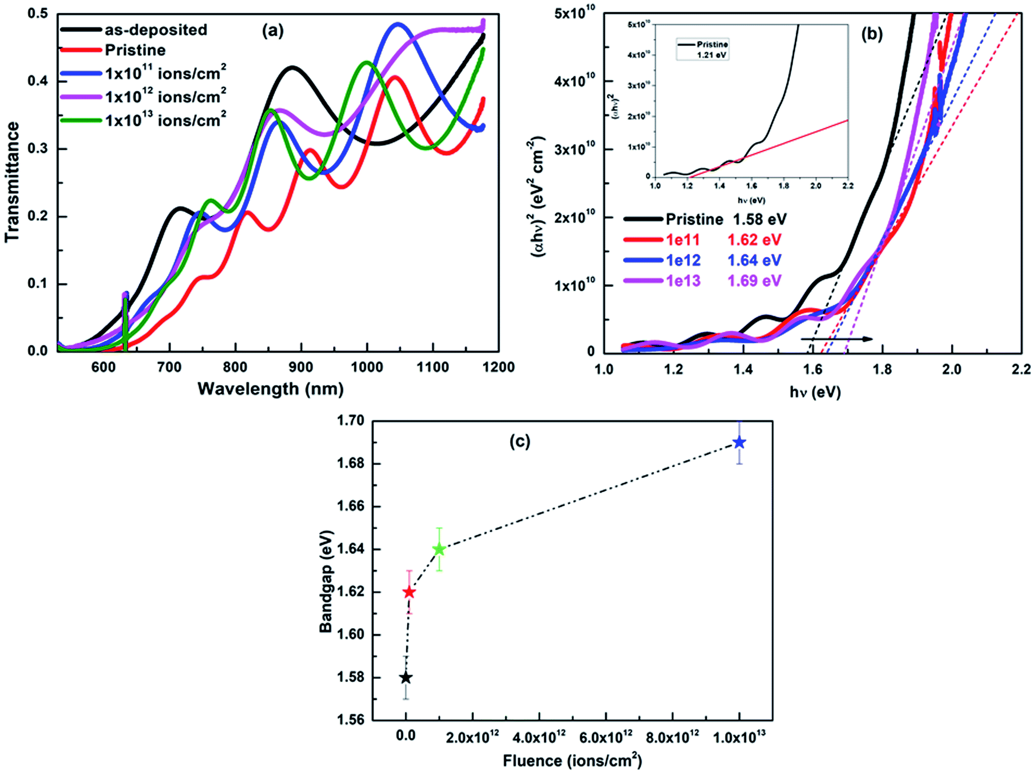 | ||
| Fig. 5 (a) Transmittance spectra of the as-deposited amorphous film, annealed film, and 120 MeV Ag irradiated film at fluences 1 × 10¹¹, 1 × 10¹², and 1 × 10¹³ ion cm−2 (b) hν vs. (αhν)2 plot of pristine and irradiated AgInSe2 thin films. The inset shows the extraction of the fundamental bandgap of AgInSe2 by linear fitting of the oscillatory region. (c) Bandgap variation with fluence. | ||
The amplitude of oscillation interestingly did not follow a monotonic variation with irradiation fluence. It showed a sharp decrease at the intermediate fluence of 1 × 10¹² ions per cm2 and then regained its initial value at high ion fluences (1 × 10¹³ ions per cm2). The amplitude of oscillations directly relates to the reflection of the radiation from the surface of the film and the film substrate interface and hence to their smoothness. In addition to creating amorphous columns along their path, irradiation by 120 MeV Ag ions is also expected to corrugate these reflecting surfaces and destroy their smoothness, as seen in many SHI irradiated systems.41,42 At low ion fluences, where tracks do not overlap, these corrugations would be more due to random protrusion of materials from the track region43 or even due to materials sputtered out of the point of impact of the ions on the surface.44,45 As a consequence, the amplitude of the oscillation is reduced at the fluence of 1 × 10¹² ions cm−2, where the surface will be highly roughened due to incomplete overlap of ion tracks, leading to the reduced amplitude of oscillations as observed (Fig. 5a). At the fluence ten times higher than this value, a complete overlap of ion tracks would lead to the flow of materials and smoothening of the surface, as reported,46–49 which would result in increased amplitude of oscillations as observed (Fig. 5a).
The bandgap (Eg) was estimated from the absorption spectra, which in turn was obtained from the transmission spectra following the relation of the absorption coefficient (a) with transmittance (T)50 for a film of thickness ‘d’, as given below.
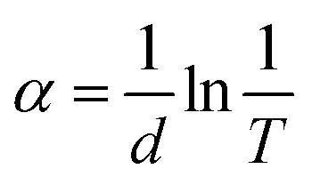 | (2) |
The AgInSe2has three bandgaps, i.e., fundamental bandgap (1.24 eV), spin–orbit splitting band gap (1.34 eV), and crystal field split band gap (1.6 eV).51 These were determined using the Tauc relation52
| αhν = B(hν − Eg)n | (3) |
Extrapolating the best fit to the Tauc plot hν versus (αhν)2 to the energy axis for zero absorption coefficients, as shown in Fig. 5b, gave the bandgap of the pristine AgInSe2 film and those irradiated at different 120 MeV Ag ion fluences. The bandgap of the pristine film was found to be 1.58 eV. This value matches with that due to crystal field splitting of the uppermost valence band.51 The fluence dependence of the bandgap of AgInSe2 (Fig. 5c) clearly indicates its increase from 1.58 eV for the pristine film to 1.69 eV for the film irradiated at the high fluence of 1 × 10¹³ ions per cm2. As stated above, the FESEM study showed a decrease in particle size with increasing irradiation fluence (Fig. 4b). So, the observed increase of the bandgap at high ion fluences is a consequence of the quantum confinement observed in small size particles.53,54
The reported spin–orbit splitting band gap (1.34 eV) could not be extracted in the present study due to the onset of interference fringes in this energy region. The presence of the same interference fringes also did not permit a straightforward determination of the fundamental bandgap from the absorption curves in the low-energy region. Had the surface not been smooth, we would have a linear decrease of the absorption with decreasing energy instead of the interference fringes. We, therefore, did a linear fitting of the region containing interference pattern and extracted the bandgap from the intersection of this line with the energy axis as shown in the inset of Fig. 5a as discussed in our previous paper.30 This bandgap was found to be 1.21 eV for the pristine film, which matches with the reported fundamental bandgap of 1.24 eV.55
3.7. Electrical conductivity by Hall measurement
The electrical parameters like Hall mobility (μ), resistivity (ρ), conductivity (σ), and the carrier concentration (n) of AgInSe2 thin films were determined by Hall measurement. These parameters are given in Table 2. The negative sign of the Hall coefficient indicates the n-type conductivity of films. This result agrees with the negative value of the off-stoichiometry parameter Δy (= [2Se/(Ag + 3In)] − 1) estimated from the EDXRF compositional analysis. Fig. 6 represents the variation of the mobility and carrier concentration of the AgInSe2 film with 120 MeV Ag ion irradiation fluence. This figure shows the increment in mobility with irradiation fluence up to 1 × 10¹² ions per cm2, which may be due to the ionization induced recovery of intrinsic defects during film deposition processes and then mobility reduced at a fluence 1 × 10¹³ ions per cm2, which may be due to the accumulation of displacement-induced defects in the thin film.56 The electrical conductivity is proportional to the product of mobility and carrier concentration in a material. In polycrystalline materials, generally, grain boundaries and confined interface charges produce inter-grain band bending and potential barriers.57 Electrons may be trapped in these potential wells between grain boundaries and could not contribute to the conduction mechanism. Upon irradiation, there is a significant rise in carrier concentration, and hence conductivity is improved drastically. Since mobility is inversely proportional to the carrier concentration, the variation in the carrier concentration with fluence is reversed as the variation of mobility with fluence. The Hall conductivity is directly proportional to the Hall mobility and carrier concentration. Thus, at a low fluence regime, the improvement in conductivity enhanced the carrier concentration and suppressed the same at high ion fluence, where amorphization sets in. The Hall coefficient is negative in all the films due to n-type conductivity because of electrons as charge carriers.| Sample | Mobility (cm2 V−1 S−1) | Hall coefficient | Conductivity (Ω cm)−1 | Carrier concentration (cm−3) |
|---|---|---|---|---|
| Pristine | 32.54 | −771 | 4.507 × 10⁻³ | 8.646 × 10¹⁴ |
| 1 × 10¹¹ ions per cm2 | 143.1 | −7638 | 2.286 × 10⁻² | 8.173 × 10¹⁴ |
| 1 × 10¹² ions per cm2 | 444.1 | −9193 | 2.680 × 10⁻² | 6.790 × 10¹⁴ |
| 1 × 10¹³ ions per cm2 | 30.16 | −7354 | 4.102 × 10⁻³ | 8.488 × 10¹⁴ |
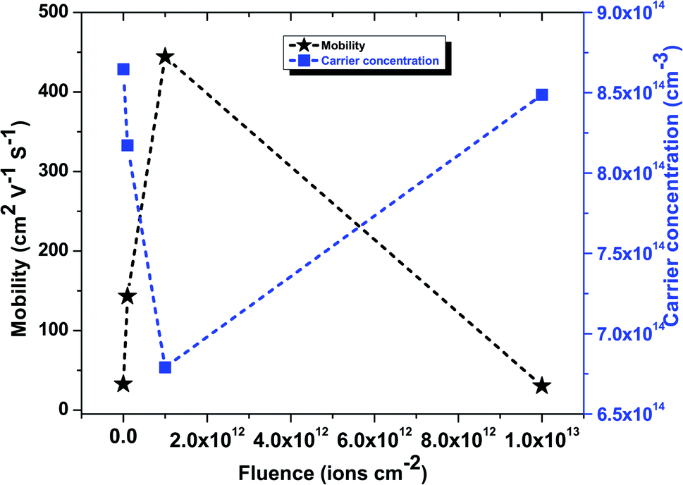 | ||
| Fig. 6 Variation of mobility and carrier concentration with 120 MeV Ag ion irradiation fluences. | ||
4. Conclusion
Thermally evaporated AgInSe2 thin films annealed at 200 °C were irradiated by 120 MeV Ag ions at different fluences. The GIXRD study revealed the creation of amorphous latent tracks along the path of 120 MeV Ag ions in the AgInSe2 thin films. Poisson's fitting of the variation of the area under the GIXRD peaks with ion fluence gave the radius of the tracks as 5.8 nm. The Raman spectroscopy of these samples also showed irradiation-induced amorphization of AgInSe2 films at high fluence. Microstructural analysis by FESEM indicated irradiation-induced fragmentation of grains leading to uniform grain size distribution as compared to the large-sized particles with widely varying particle size distribution in the unirradiated film. Conforming to the reduction of particle size in irradiated films, the UV-visible study indicated the increase in the electronic bandgap due to quantum confinement in small-sized particles obtained at high ion fluences. Both the EDXRF and Hall measurement studies indicated the n-type conductivity of films. The change in both optical and electrical parameters with different ion fluences is suitable for optoelectronic applications.Author contributions
R. Panda: writing – original draft, software, data curation, investigation. S. A. Khan: data collection, investigation. U. P. Singh: visualization, investigation. R. Naik: conceptualization, methodology, writing – review & editing, supervision. N. C. Mishra: conceptualization, review, and editing.Conflicts of interest
There are no conflicts of interest for this manuscript.Acknowledgements
The author, Ms. Panda, thanks IUAC New Delhi for the SHI facility and NISER for the FESEM measurements.References
- D. K. Avasthi and G. K. Mehta, Materials Engineering with Swift Heavy Ions, Springer Netherlands, 2011 Search PubMed.
- A. Meftah, F. Brisardand, J. M. Costantini, M. Hage-Ali, J. P. Stoquert, F. Studer and M. Toulemonde, Swift heavy ions in magnetic insulators: A damage-cross-section velocity effect, Phys. Rev. B: Condens. Matter Mater. Phys., 1993, 48(2), 920 CrossRef CAS PubMed.
- P. Sigmund, Energy density and time constant of heavy ion induced elastic collision spikes in solids, Appl. Phys. Lett., 1974, 25, 169 CrossRef.
- G. S. Was, Ion beam modification of metals: Compositional and microstructural changes, Prog. Surf. Sci., 1990, 32, 211–332 CrossRef.
- Y. Zhang, T. Varga, M. Ishimaru, P. D. Edmondson, H. Xue, P. Liu and W. J. Weber, Competing effects of electronic and nuclear energy loss on microstructural evolution in ionic-covalent materials, Nucl. Instrum. Methods Phys. Res., Sect. B, 2014, 327, 33–43 CrossRef CAS.
- A. Barbu, A. Dunlop, D. Lesueur and R. S. Averbac, Latent tracks do exist in metallic materials, Europhys. Lett., 1991, 15(l), 37–42 CrossRef CAS.
- A. Dunlop, G. Jaskierowicz and S. Della-Negra, Latent track formation in silicon irradiated by 30 MeV fullerenes, Nucl. Instrum. Methods Phys. Res., Sect. B, 1998, 146, 302–308 CrossRef CAS.
- M. Toulemonde, A. Benyagoub, C. Trautmann, N. Khalfaoui, M. Boccanfuso, C. Dufour, F. Gourbilleau, J. J. Grob, J. P. Stoquert, J. M. Costantini, F. Haas, E. Jacquet, K. O. Voss and A. Meftah, Dense and nanometric electronic excitations induced by swift heavy ions in an ionic CaF crystal: Evidence for two thresholds of damage creation, Phys. Rev. B: Condens. Matter Mater. Phys., 2012, 85, 054112 CrossRef.
- H. Rath, P. Dash, U. P. Singh, D. K. Avasthi, D. Kanjilal and N. C. Mishra, Modification of the microstructure and electronic properties of rutile TiO2 thin films with 79 MeV Br ion irradiation, Nucl. Instrum. Methods Phys. Res., Sect. B, 2015, 365, 553–559 CrossRef CAS.
- A. Dunlop, D. Lesueur, J. Morillo, J. Dural, R. Spohr and J. Vetter, High electronic excitations and damage production in GeV-ion-irradiated metals, Nucl. Instrum. Methods Phys. Res., Sect. B, 1990, 48, 419 CrossRef.
- A. Iwase, S. Sakaki, T. Iwata and T. Nihira, Anomalous reduction of stage-I recovery in nickel irradiated with heavy ions in the energy range 100–120 MeV, Phys. Rev. Lett., 1987, 58, 2450 CrossRef CAS PubMed.
- X. Hou, H. Ma, F. Liu, J. Deng, Y. Ai, X. Zhao, D. Mao, D. Li and B. Liao, Synthesis of Ag ion-implanted TiO2 thin films for antibacterial application and photocatalytic performance, J. Hazard. Mater., 2015, 299, 59–66 CrossRef CAS PubMed.
- T. S. Kavetskyy et al. in Formation of a Periodic Structure in a Chalcogenide Film Substrate by Silver Ion Implantation, Advanced Nanotechnologies for Detection and Defence against CBRN Agents, ed. Petkov P., Tsiulyanu D., Popov C. and Kulisch W., 2018, pp. 49–54 Search PubMed.
- K. L. Chopra, P. Paulson and V. Dutta, Thin-film solar cells: An overview, Prog. Photovoltaics Res. Appl., 2004, 12, 69–92 CrossRef CAS.
- P. P. Ramesh, M. O. Hussain, S. Uthanna, S. B. Naidu and J. P. Reddy, Photovoltaic performance of p-AgInSe2/n-CdS thin film heterojunctions, Mater. Lett., 1997, 34, 217 CrossRef.
- D. Pathak, T. Wagner, T. Adhikari and J. M. Nunzi, Photovoltaic performance of AgInSe2-conjugated polymer hybrid system bulk heterojunction solar cells, Synth. Met., 2015, 199, 87–92 CrossRef CAS.
- H. I. Elim, W. Ji, M. T. Ng and J. J. Vittal, AgInSe2 nanorods: A semiconducting material for saturable absorber, Appl. Phys. Lett., 2007, 90, 033106 CrossRef.
- N. D. Abazovic, M. I. Comor, M. N. Mitric, E. Piscopiello, T. Radetic, I. A. Jankovic and J. M. Nedeljkovic, Ligand mediated synthesis of AgInSe2 nanoparticles with tetragonal/orthorhombic crystal phases, J. Nanopart. Res., 2012, 14, 810 CrossRef.
- H. Mustafa, D. Hunter, A. K. Pradhan, U. N. Roy, Y. Cui and A. Burger, Synthesis and characterization of AgInSe2 for application in thin film solar cells, Thin Solid Films, 2007, 515, 7001–7004 CrossRef CAS.
- R. Naik, S. Jena, R. Ganesan and N. K. Sahoo, Effect of laser irradiation on optical properties of Ge12Sb25Se63 amorphous chalcogenide thin films, Indian J. Phys., 2015, 89(10), 1031–1040 CrossRef CAS.
- D. Sahoo, P. Priyadarshini, A. Aparimita, D. Alagarasan, R. Ganesan and R. Naik, Role of annealing temperature on optimizing the linear and nonlinear optical properties of As40Se50Ge10 films, RSC Adv., 2020, 10, 26675–26685 RSC.
- A. K. Anbalagan, C. Y. Jao, M. Syabriyana, C. L. Fan, S. Gupta, M. Chaudhary, Y. Chueh, N. H. Tai and C. H. Lee, Influence of gamma-ray irradiation and post-annealing studies on pentacene films: the anisotropic effects on structural and electronic properties, RSC Adv., 2020, 10, 21092–21099 RSC.
- M. G. Shin, S. H. Hwang, H. S. Cha, H. S. Jeong, D. H. Kim and H. I. Kwon, Effects of proton beam irradiation on the physical and chemical properties of IGTO thin films with different thicknesses for thin-film transistor applications, Surf. Interfaces, 2021, 23, 100990 CrossRef CAS.
- D. Pathak, R. K. Bedi, D. Kaur and R. Kumar, Fabrication of densely distributed silver indium selenide nanorods by using Ag+ ion irradiation, J. Korean Phys. Soc., 2010, 57(3), 474–479 CrossRef CAS.
- D. Pathak, R. K. Bedi, D. Kaur and R. Kumar, 200 MeV Ag+ ion beam induced modifications in AgInSe2 films deposited by hot wall vacuum evaporation method, Chalcogenide Lett., 2011, 8(1), 213–222 CAS.
- R. Panda, M. Panda, H. Rath, B. N. Dash, K. Asokan, U. P. Singh, R. Naik and N. C. Mishra, Structural and morphological modifications of AgInSe2 and Ag2Se composite thin films on 140 MeV Ni ion irradiation, Appl. Surf. Sci., 2019, 479, 997–1005 CrossRef CAS.
- P. Mallick, C. Rath, J. Prakash, D. K. Mishra, R. J. Choudhary, D. M. Phase, A. D. K. Avasthi, D. Kanjilal and N. C. Mishra, Swift heavy ion irradiation induced modification of the microstructure of NiO thin films, Nucl. Instrum. Methods Phys. Res., Sect. B, 2010, 268, 1613–1617 CrossRef CAS.
- J. F. Ziegler, M. D. Ziegler and J. P. Biersack, SRIM-The stopping and range of ions in matter, Nucl. Instrum. Methods Phys. Res., Sect. B, 2010, 268, 1818–1823 CrossRef CAS.
- J. A. Groknink and P. H. Janse, Int. J. Res. Phys. Chem. Chem. Phys., 1978, 110, 17–28 Search PubMed.
- R. Panda, U. P. Singh, R. Naik and N. C. Mishra, Low temperature synthesis of embedded AgInSe2 nano-crystallites in an amorphous matrix, AIP Conf. Proc., 2018, 2005, 030007 CrossRef CAS.
- R. Panda, M. Panda, H. Rath, U. P. Singh, R. Naik and N. C. Mishra, Annealing induced AgInSe2 formation from Ag/In/Ag/In multilayer film for solar cell absorbing layer, Opt. Mater., 2018, 84, 618–624 CrossRef CAS.
- G. K. Mehta, High energy accelerators and material science, PINSA-A: Proc. Indian Natl. Sci. Acad., Part A, 2000, 66, 653–674 CAS.
- R. Biswal, J. John, P. Mallick, B. N. Dash, P. K. Kulriya, D. K. Avasthi, D. Kanjilal, D. Behera, T. Mohanty, P. Raychaudhuri and N. C. Mishra, 200 MeV silver ion irradiation induced structural modification in thin films at 89 K: An in situ x-ray diffraction study, J. Appl. Phys., 2009, 106, 053912 CrossRef.
- H. Rath, B. N. Dash, A. Benyagoub and N. C. Mishra, Sensitivity of Anatase and Rutile Phases of TiO2 to ion irradiation: Examination of the applicability of Coulomb Explosion and Thermal Spike Models, Sci. Rep., 2018, 8, 11774 CrossRef PubMed.
- Y. Jin, K. Tang, Ch. An and L. Huang, Hydrothermal synthesis and characterization of AgInSe2 nanorods, J. Cryst. Growth, 2003, 253, 429–434 CrossRef CAS.
- A. Berthelot, S. Hemon, F. Gourbilleau, C. Dufour, E. Dooryhee and E. Paumier, Nanometric size effects on irradiation of tin oxide powder, Nucl. Instrum. Methods Phys. Res., Sect. B, 1998, 146, 437–442 CrossRef CAS.
- H. Rath, P. Dash, T. Som, J. Prakash, A. Tripathi, D. K. Avasthi, U. P. Singh and N. C. Mishra, Radiat. Eff. Defects Solids, 2011, 15, 1–7 Search PubMed.
- M. Behera, S. Behera and R. Naik, Optical bandgap tuning by laser induced Bi diffusion into As2Se3 film probed by spectroscopic techniques, RSC Adv., 2017, 7, 18428 RSC.
- A. Aparimita, C. Sripan, R. Ganesan and R. Naik, Photo-and thermally induced property change in Ag diffusion into Ag/As2Se3 thin films, Appl. Phys. A, 2018, 124, 267 CrossRef.
- H. Nyakotyo, T. S. Sathiaraj and E. Muchuweni, Effect of annealing on the optical properties of amorphous Se79Te10Sb4Bi7 thin films, Opt. Laser Technol., 2017, 92, 182–188 CrossRef CAS.
- P. C. Srivastava, V. Ganesanb and O. P. Sinha, AFM studies of swift heavy ion-irradiated surface modification in Si and GaAs, Radiat. Meas., 2003, 36, 671–674 CrossRef CAS.
- S. Vauth and S. G. Mayr, Ion bombardment induced smoothing of amorphous metallic surfaces: Experiments versus computer simulations, Phys. Rev. B: Condens. Matter Mater. Phys., 2008, 77, 155406 CrossRef.
- N. Khalfaoui, C. C. Rotaru, S. Bouffard, E. Jacquet, H. Lebius and M. Toulemonde, Study of swift heavy ion tracks on crystalline quartz surfaces, Nucl. Instrum. Methods Phys. Res., Sect. B, 2003, 209, 165–169 CrossRef CAS.
- S. Thomas, H. Thomas, D. K. Avasthi, A. Tripathi, R. V. Ramanujan and M. R. Anantharaman, Swift heavy ion induced surface modification for tailoring coercivity in Fe–Ni based amorphous thin films, J. Appl. Phys., 2009, 105, 033910 CrossRef.
- D. Gupta, M. Chawla, R. Singhal and S. Aggarwal, Nanoscale structural defects in oblique Ar+ sputtered Si(111) surfaces, Sci. Rep., 2019, 9, 15531 CrossRef PubMed.
- A. Gupta and D. K. Avasthi, Large electronically mediated sputtering in gold films, Phys. Rev. B: Condens. Matter Mater. Phys., 2001, 64, 155407 CrossRef.
- P. Dash, P. Mallick, H. Rath, B. N. Dash, A. Tripathi, J. Prakash, D. K. Avasthi, P. V. Satyam and N. C. Mishra, Surface modifications of ultra-thin gold films by swift heavy ion irradiation, Indian J. Phys., 2010, 84(10), 1391–1397 CrossRef CAS.
- H. Thomas, S. Thomas, R. V. Ramanujan, D. K. Avasthi, I. A. A. Omari, S. Al-harthi and M. R. Anantharaman, 200 MeV Ag15+ ion beam irradiation induced modifications in spray deposited MoO3 thin films by fluence variation, Nucl. Instrum. Methods Phys. Res., Sect. B, 2012, 287, 85–90 CrossRef CAS.
- R. Rathika, M. Kovendhan, D. Paul Joseph, K. Vijayarangamuthu, A. Sendil Kumar, C. Venkateswaran, K. Asokan and S. Johnson Jeyakumar, 200 MeV Ag15+ ion beam irradiation induced modifications in spray deposited MoO3 thin films by fluence variation, Nucl. Eng. Technol., 2019, 51(8), 1983–1990 CrossRef CAS.
- A. Aparimita, M. Behera, C. Sripan, R. Ganesan, S. Jena and R. Naik, Effect of Bi addition on the optical properties of Ge30Se70-xBix thin films, J. Alloys Compd., 2018, 739, 997–1004 CrossRef CAS.
- J. L. Shay and B. Tell, Energy band structure of I–III–VI2 semiconductors, Surf. Sci., 1973, 37, 748–762 CrossRef CAS.
- J. Tauc, Optical Properties of Solids, North-Holland, Amsterdam, 1970, p. 159 Search PubMed.
- M. B. Sahana, C. Sudakar, G. Setzler, A. Dixit, J. S. Thakur, G. Lawes, V. M. Naik and P. P. Vaishnava, Bandgap engineering by tuning particle size and crystallinity of SnO2–Fe2O3 nanocrystalline composite thin films, Appl. Phys. Lett., 2008, 93, 231909 CrossRef.
- B. Venugopal, B. Nandan, A. Ayyachamy, V. Balaji, S. Amirthapandian, B. K. Panigrahi and T. Paramasivam, Influence of manganese ions in the band gap of tin oxide nanoparticles: structure, microstructure and optical Studies, RSC Adv., 2014, 4, 6141–6150 RSC.
- D. Pathak, R. K. Bedi and D. Kaur, Growth of AgInSe2 on Si(100) substrate by thermal evaporation technique, Appl. Phys. A, 2009, 95, 843–847 CrossRef CAS.
- G. Fu, L. Zuo, J. Lian, Y. Wang, J. Chen, J. Longtin and Z. Xiao, Ion beam irradiation effect on thermoelectric properties of Bi2Te3 and Sb2Te3 thin films, Nucl. Instrum. Methods Phys. Res., Sect. B, 2015, 358, 229–235 CrossRef CAS.
- R. Rathika, M. Kovendhan, D. Paul Joseph, R. Pachaiappan, A. Sendil Kumar, K. Vijayarangamuthu, C. Venkateswaran, K. Asokan and S. J. Jeyakumar, Nucl. Eng. Technol., 2020, 52, 2585–2593 CrossRef CAS.
| This journal is © The Royal Society of Chemistry 2021 |