
 Open Access Article
 This Open Access Article is licensed under a Creative Commons Attribution-Non Commercial 3.0 Unported Licence
Time dependence of domain structures in potassium sodium niobate-based piezoelectric ceramics
Jia Yang†
a,
Zhipeng Gao† *ab,
Yi Liua,
Zhengwei Xiongb,
Faqiang Zhangc,
Zhengqian Fu*c,
Fangfang Xuc,
Xuefeng Chenc,
Qiang Yanga and
Leiming Fangd
*ab,
Yi Liua,
Zhengwei Xiongb,
Faqiang Zhangc,
Zhengqian Fu*c,
Fangfang Xuc,
Xuefeng Chenc,
Qiang Yanga and
Leiming Fangd
aInstitute of Fluid Physics, China Academy of Engineering Physics, Mianyang, 621900, China. E-mail: z.p.gao@foxmail.com
bJoint Laboratory for Extreme Conditions Matter Properties, Southwest University of Science and Technology, Mianyang 621010, China
cThe Key Lab of Inorganic Functional Materials and Devices, Shanghai Institute of Ceramics, Chinese Academy of Sciences, Shanghai 200050, China. E-mail: fmail600@126.com
dInstitute of Physics Nuclear and Chemistry, China Academy of Engineering Physics, Mianyang, 621900, China
First published on 4th June 2021
Abstract
Piezoelectric materials, which can convert energy between electrical and mechanical forms, are widely used in modern industry. (K,Na)NbO3-based ceramics have attracted extensive attention due to their excellent performance characteristics among the lead-free materials. Piezoelectric properties are closely related to ferroelectric domain structures including the domain morphology and domain wall motion. However, time dependence of ferroelectric domains in (K,Na)NbO3-based ceramics has barely been studied. Here, we synthesized Li-doped KNN ceramics. The morphologies and crystallographic parameters of the domain structures were characterized. Two ferroelectric domains, the 60°/120° and 180° domains, were identified in the ceramic. Surprisingly, the domain structure changed naturally as time passed, and most of the change occurred in the 180° domain wall, while the 60°/120° domains remained nearly unchanged. Our results are different from those of previous studies, which showed that the non-180° domain wall was more prone to movement than the 180° domain wall.
1. Introduction
Piezoelectric materials, which convert energy between electrical and mechanical forms, are widely used in modern technologies such as electronics, sensors, drivers, and resonators.1–3 Lead-based piezoelectric ceramics comprise the main commercial market due to their high Curie temperatures (TC) and piezoelectric coefficients (d33).4,5 However, the toxicity of the lead commonly used in piezoelectric devices is a serious threat to the environment. There is a trend toward the use of environmentally friendly lead-free piezoelectric ceramics. Therefore, (K,Na)NbO3-based materials (KNN materials) have attracted extensive attention due to their good overall performance characteristics, including their high piezoelectric constants and Curie temperatures. Some properties of (K,Na)NbO3 compounds can even match those of PZTs.6–10Many studies have been performed to improve the piezoelectric properties and TC values of these materials.7–15 Chemical doping is one of the most common and effective methods of improving KNN performance. Li, Ta, Sb, and other elements are often used to improve the piezoelectric constants in order to adjust the orthogonal–tetragonal phase transition (To–Tt) from 200 °C to room temperature.10–14 For example, Lin et al.11 doped Li and Ta to raise the d33 values of KNN compounds from 93 pC N−1 to 208 pC N−1. Saito et al.14 improved the d33 of KNN to 416 pC N−1 using a Li–Ta–Sb multi-doping strategy. The literature shows that Li elemental doping can improve the TC values of KNN ceramics, but the TC values of KNN ceramics are typically reduced when the other elements are involved. For example, the TC can increase to more than 500 °C when the Li content is approximately 10 mol%.6
Fundamentally, all of these properties, including the piezoelectric properties and temperature stability, are closely related to the ferroelectric domain structures of the KNN ceramics, including domain morphologies, domain switching, and domain wall motion.10,16,17 Cho et al.18 studied the domain structures and morphologies of Li-doped KNN ceramics using Piezoelectric Force Microscopy (PFM). Zhang et al.19 investigated the domain morphologies of pure KNN ceramics using scanning electron microscopy (SEM) and performed a detailed analysis of their domain sizes and crystallographic characteristics. Their results show that there are two types of domain structures present in the grains: one that consists of 90°, 60°, and 120° domain boundaries and another that consists of 180°, 90°, and 120° domain boundaries. Bah et al.20 revealed hierarchical domain structures in KNN ceramics via transmission electron microscopy (TEM). They analyzed the anti-phase domain boundary (APB) and revealed that the APB results from small mismatches between interfacial structures. In recent years, in situ studies have allowed important progress to been made in understanding of KNN ceramic domain structures. For example, Liu et al.21 found that laminar domains in Mn-doped KNN ceramics can transform into twinned domains as the temperature decreases. The laminar domains can grow in size when the applied electric field decreases. Wu et al.22 found that KNN ceramic temperature stability can be enhanced by adjusting the phase boundaries. In addition, Tan et al.23 used in situ electric field experiments to reveal that domain walls play an important role in KNN ceramic piezoelectric stability.
Furthermore, the time-dependent behaviors of the ferroelectric domains in KNN ceramics can have substantial influence on their aging and fatigue properties. This cannot be ignored in applications. However, although the various ferroelectric properties and structures have been investigated, the time dependence of ferroelectric domains in KNN materials has barely been studied. In this study, we synthesized Li-doped KNN ceramics. The morphologies and crystallographic characteristics of the domain structures were characterized via TEM and changes in the domain structure with time were analyzed. The results might help researchers to understand the aging behavior of KNN ceramics and guide materials design for applications.
2. Materials and methods
The (K0.45Na0.55)0.96Li0.04NbO3 (KNLN) ceramics were prepared via the traditional solid reaction method.24–27 K2CO3 (99.0%), Na2CO3 (99.8%), Li2CO3 (98.0%), and Nb2O5 (99.5%) were used as raw materials and weighed according to the chemical ratio. The raw mixed powder was put into the nylon tank for mixing with ethanol as ball milling medium. The raw powder was mixed by ball milling for 4 hours and then dried in 65 °C for 8 hours. The mixed powder was then pre-sintered in an alumina crucible at 850 °C for 4 h for reaction. The synthesized KNLN powder was subsequently obtained via ball grinding. The obtained KNLN powder was granulated by adding binder (PVA) and a pressure of 200 MPa was used to prepare the cylindrical green body. The ceramic green body was calcined at approximately 1000 °C for 4 h in a crucible filled with the KNLN powder to avoid volatilization of the alkali metal elements. An X-ray diffractometer (XRD, λ = 0.1542 nm, D/Max-2550V, Rigaku, Japan) was used to analyze the sample structure.28–30 The grain morphologies were characterized via scanning electron microscope/SEM (FEI Magellan 400, Oregon, USA). Transmission electron microscope/TEM (JEOL JEM-2100F) with a working voltage of 200 kV was used to reveal the ceramic microstructures. The TEM sample was prepared via mechanical thinning followed by Ar+ milling.3. Results and discussion
Fig. 1(a) shows the XRD pattern of the as-sintered KNLN ceramic. The pattern shows that the as-sintered ceramic has a single phase. The XRD refinement was carried out shown as the inset of Fig. 1(a).31–33 The result indicates this ceramic has a typical perovskite structure (orthorhombic) with point group of Amm2, and the lattice parameters are (a, b, c) = (3.94 Å, 5.65 Å, 5.68 Å). This is in good agreement with the previous literatures.9,10,34 | ||
| Fig. 1 (a) XRD pattern of the as-sintered KNLN ceramic and the inset shows the refinement data; (b) temperature-dependent permittivity of the KNLN ceramic at various frequencies; (c) and (d) SEM images of the ceramic showing grain morphologies; the inset of (c) is a schematic diagram of a grain with a typical perovskite cubic shape; (e) TEM photographs of a KNLN grain; the left-bottom inset of (e) shows the selected electron diffraction patterns in the [001] direction, while the top-right inset of (e) is a magnified image of a pore in the grain. | ||
Fig. 1(b) shows the temperature dependence of the dielectric constant at 10 kHz, 100 kHz, and 1000 kHz, respectively. It is obvious that two phase-transition peaks can be found. The first broad peak located at approximately 130 °C is related to the polymorphic phase transition from orthorhombic to tetragonal (TO–T). The second sharp peak, which is the ferroelectric–paraelectric phase transition temperature (TC) of the KNLN ceramic, is located at approximately 452 °C. From these results, it is clear that the prepared ceramic is pure and has no second phase.
Fig. 1(c) and (d) show SEM micrographs of ceramic grains with typical perovskite-cubic shapes and an average size of approximately 10 µm. Fig. 1(e) shows a TEM image of a KNLN grain. The left-bottom inset of Fig. 1(e) is the selected electron diffraction pattern, which shows that the flat surface seen in Fig. 1(e) is the {001} surface of a single crystal. It is worth noting that the KNLN ceramic has an orthorhombic structure, but the grains grow in a perovskite-cubic shape with surfaces of {100}, {010}, and {001} [inset of Fig. 1(c)].
There are some pores wrapped inside the grain [Fig. 1(e)]. The top-right inset of Fig. 1(e) is a magnified image of a pore. The pores in this area occasionally fail to penetrate the grain, with a layer of samples on its upper or lower side. We can see that the pores in the grain have six contact surfaces with smooth edges and corners, all of which are {100} surfaces. The parallel lines seen in the pore area might be the domain structure. The grains and pores can form regular polyhedral shapes, thus indicating that liquid-phase mass transfer occurs during grain growth.35 These phenomena can be explained by a grain-growth liquid-phase mass transfer process that occurs faster than pore elimination, thus producing pores wrapped inside grains. Furthermore, the uniformity of the liquid-phase mass transfer process causes the pores in the grains to have regular shapes. The liquid phase present during grain growth of KNLN ceramics might form due to the alkali metal oxide, which has a relatively low melting point and forms a liquid phase during sintering.
Fig. 2(a) shows a TEM image of a triangular grain with a grain size of approximately 8 µm and straight grain boundaries. The grain boundaries are marked by yellow lines. Abundant patterns related to the ferroelectric domains are seen inside the grain. Fig. 2(b) and (c) show selected-area electron diffraction (SAED) patterns projected along the [111] and [112] zone axes, respectively. From these images and patterns, we can see that there is a single grain and the patterns in the grain are from the ferroelectric domain structure rather than from overlapping grains. Fig. 2(d) and (e) show the spatial orientations of various domain walls and trace lines. Fig. 2(f) shows the non-180° domain structure models in the triangular grain with indexing of the domain walls and trace lines.
 | ||
| Fig. 2 (a) TEM image of a triangular grain with straight grain boundaries. The grain boundaries are marked by yellow lines; (b) and (c) the corresponding selected-area electron diffraction (SAED) patterns projected along the [111] and [112] zone axes, respectively; (d)–(f) the non-180° domain structure model in the triangular grain; (d) and (e) the spatial orientations of different domain walls and trace lines; (f) indexing of the domain walls and trace lines. | ||
In orthorhombic symmetry, the orientation of spontaneous polarization is along the 〈110〉 direction. Consequently, the permissible boundaries are {100} planes for 90° domains; {110} or {hkk} planes for 60° and 120° domains; and arbitrary for 180° domains. Specifically, the Miller indices of the {hkk} walls are irrational and depend on spontaneous strain tensor coefficients.36,37 The trace lines of non-180° domain boundaries can be approximated based on SAED patterns along the [111] and [112] zone axes. The observed [1![[2 with combining macron]](https://www.rsc.org/images/entities/char_0032_0304.gif) 1] and [11] vectors indicate that the grain surface is close to the [111] plane. This matches well with the triangular morphology. Correspondingly, the domain boundaries are located on {110} [Fig. 2(d) and (e)]. The domain boundaries with 〈110〉-oriented trace lines are edge-on with the view direction between the [111] and [112] zone axes, where the (11l) and (1kl) planes are satisfied by intersecting with the grain surface.
1] and [11] vectors indicate that the grain surface is close to the [111] plane. This matches well with the triangular morphology. Correspondingly, the domain boundaries are located on {110} [Fig. 2(d) and (e)]. The domain boundaries with 〈110〉-oriented trace lines are edge-on with the view direction between the [111] and [112] zone axes, where the (11l) and (1kl) planes are satisfied by intersecting with the grain surface.
Fig. 3(a)–(d) present high-resolution TEM images of the grain. Based on the results from Fig. 2 and 3, we can determine that there are two ferroelectric domains in this KNLN grain. All of the waving boundaries in Fig. 3(a)–(d) can be 180° domains; some of them are marked by a yellow oval. The non-180° domain boundaries observed in Fig. 3 are 60°/120° domains and are highlighted by parallel lines. The 60°/120° domain walls are straight and exhibit two morphologies. One has a laminar structure with a width of approximately 35 nm, while the other has width of approximately 300 nm. The grain boundaries are marked by straight, red lines in Fig. 3(a) and are clearly different from the domain walls.
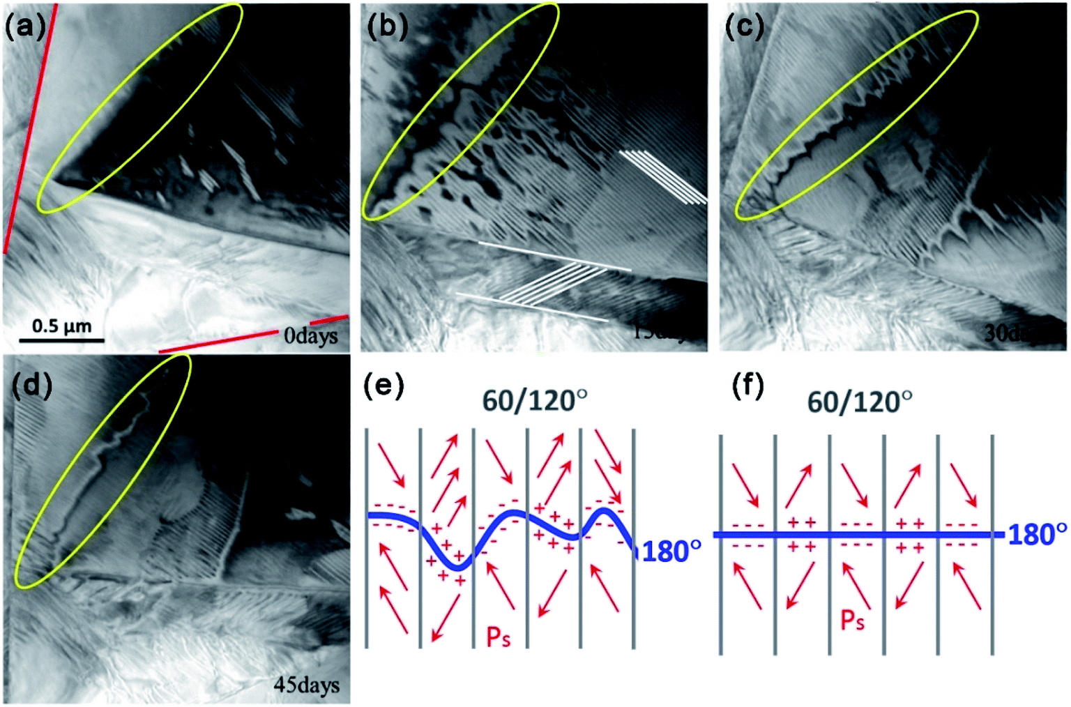 | ||
| Fig. 3 Evolution of the domain structure in a triangular grain over time. (a)–(d) TEM images are taken along similar orientations at time intervals of 15 d. The slight rotation between different images is caused by TEM holder sample positions that differ slightly between experiments. The grain boundaries are marked by straight, red lines in (a). The 60°/120° and 180° domains are indicated in (b) by parallel, white lines and yellow ovals, respectively. (e) and (f) A proposed model of the domain walls shows the domain structure (e) before and (f) after aging. | ||
In order to investigate domain structure evolution in the triangular grain, we fixed the observation area and applied a time interval of 15 d. The domain structures in the triangular grain exhibit significant differences every 15 d when observed at the same location under consistent conditions. No driving force such as an electric field or temperature change is present. Careful analysis of the domain morphologies shows that domain structure evolution occurs mainly via 180° domain wall changes, but the 60° domains remain nearly unchanged. As time passes, the waving 180° domain wall shrinks and the 180° domain wall area decreases.
Fig. 3(e) and (f) propose a simple model that seeks to explain this change in the 180° domain walls. Since formation of the 180° domain is related to the depolarization energy,38,39 it is likely that this phenomenon is caused by a change in the bound state or distribution of space charge.39,40 As shown in Fig. 3(e) and (f), electric charges with the same sign accumulate at both sides of the 180° domain walls. This might lead the wall area to exhibit relatively high energy and be unstable. As time passes, the 180° domain walls decrease the unstable area and lower the energy by shrinking rather than remaining unchanged. This process is observed as the 180° domain wall moving from Fig. 3(e) and (f). These results reveal that the 180° domain structure in KNLN ferroelectric ceramics evolves naturally even without electrical poling.
The domain structure of a ferroelectric ceramic is generally disordered before electrical poling and there is no net spontaneous polarization. After poling, the electric dipole is arranged along the direction of the electric field. When the electric field is removed, the electric dipole needs high energy to maintain the saturated polarization state, so it spontaneously reorients towards the disordered state.39–42 This process is known as aging behavior.43 Previous studies have shown that the change in the 180° domain does not produce strain during reorientation, while changes in non-180° domains produce strain that leads to changes in performance.44,45 Therefore, it is widely believed that the aging phenomenon is caused only by flipping of non-180° domains.40,43–46 However, our experiments show that the 180° domain in KNLN ceramics changes with time, and that this might influence aging behavior. This result can help researchers to understand aging behavior in KNN ceramics and guide future materials applications.
In this study, we prepared Li-doped KNN ceramics and the morphologies of the ferroelectric domain structures were characterized. Two ferroelectric domains, the 60°/120° and 180° domains, were identified in this ceramic. The domain structure would change as time passed. Most of the change occurred in the 180° domain wall, while the 60°/120° domains remained nearly unchanged. These results are different from those of previous studies, which showed that the non-180° domain wall was more prone to movement than the 180° domain wall. This result can help to promote understanding of KNN ceramic aging behavior and guide future material applications.
Data availability
The data that support the findings of this study are available from the corresponding author upon reasonable request.Conflicts of interest
There are no conflicts to declare.Acknowledgements
This work was supported by the CAEP Foundation (2018AB02) and National Natural Science Foundation of China (11904299, U1930124).References
- K. Wang, Z. Shen, B. Zhang and J. Li, J. Inorg. Mater., 2014, 29(1), 13–22 CrossRef CAS.
- M. Acosta, N. Novak, V. Rojas, S. Patel, R. Vaish, J. Koruza and J. Rödel, Appl. Phys. Rev., 2017, 4(4), 041305 Search PubMed.
- L. Xiang, X. Zhang and J. Wu, J. Mater. Chem. A, 2020, 8(20), 10026–10073 RSC.
- S. E. Park and T. R. Shrout, J. Appl. Phys., 1997, 82(4), 1804–1811 CrossRef CAS.
- S. W. Choi, R. T. Shrout, S. J. Jang and A. S. Bhalla, Ferroelectrics, 1989, 100(1), 29–38 CrossRef CAS.
- Y. Guo, K. Kakimoto and H. Ohsato, Appl. Phys. Lett., 2004, 85(18), 4121–4123 CrossRef CAS.
- J. Li, K. Wang, B. Zhang and L. Zhang, J. Am. Ceram. Soc., 2006, 89(2), 706–709 CrossRef CAS.
- D. W. Baker, P. A. Thomas, N. Zhang and A. M. Glazer, Appl. Phys. Lett., 2009, 95(9), 091903 CrossRef.
- J. Li, K. Wang, F. Zhu, L. Cheng and F. Yao, J. Am. Ceram. Soc., 2013, 96(12), 3677–3696 CrossRef CAS.
- K. Wang and J. Li, Adv. Funct. Mater., 2010, 20(12), 1924–1929 CrossRef CAS.
- D. Lin, K. W. Kwok and H. L. W. Chan, J. Appl. Phys., 2007, 102(3), 034102 CrossRef.
- P. Palei, P. Kumar and D. K. Agrawal, Journal of Microwave Power and Electromagnetic Energy, 2012, 46(2), 76–82 Search PubMed.
- E. Hollenstein, D. Damjanovic and N. Setter, J. Eur. Ceram. Soc., 2007, 27(13), 4093–4097 CrossRef CAS.
- Y. Saito, H. Takao, T. Tani, T. Nonoyama, K. Takatori, T. Homma, T. Nagaya and M. Nakamura, Nature, 2004, 432(7013), 84–87 CrossRef CAS PubMed.
- J. Rödel, W. Jo, K. T. Seifert, E. Anton, T. Granzow and D. Damjanovic, J. Am. Ceram. Soc., 2009, 92(6), 1153–1177 CrossRef.
- J. E. García, J. D. S. Guerra, E. B. Araújo and R. Pérez, J. Phys. D: Appl. Phys., 2009, 42(11), 115421 CrossRef.
- P. Zheng, J. Zhang, Y. Tan and C. Wang, Acta Mater., 2012, 60(13–14), 5022–5030 CrossRef CAS.
- J. H. Cho, N. R. Yeom, S. J. Kwon, Y. J. Lee, Y. H. Jeong, M. P. Chun, J. H. Nam, J. H. Paik and B. I. Kim, J. Appl. Phys., 2012, 112(5), 53 CrossRef.
- Y. Qin, J. Zhang, Y. Gao, Y. Tan and C. Wang, J. Appl. Phys., 2013, 113(20), 84 CrossRef.
- M. Bah, N. Alyabyeva, R. Retoux, F. Giovannelli, M. Zaghrioui, A. Ruyter, F. Delorme and I. Monot-Laffez, RSC Adv., 2016, 6(54), 49060–49067 RSC.
- D. Lin, S. Zhang, C. Cai and W. Liu, J. Appl. Phys., 2015, 117(7), 074103 CrossRef.
- C. Zhao, B. Wu, K. Wang, J. Li, D. Xiao, J. Zhu and J. Wu, J. Mater. Chem. A, 2018, 6(46), 23736–23745 RSC.
- Z. Fan, S. Zhang and X. Tan, J. Eur. Ceram. Soc., 2020, 40(4), 1217–1222 CrossRef CAS.
- K. Shan, Z.-Z. Yi, X.-T. Yin, D. Dastan and H. Garmestani, Dalton Trans., 2020, 49, 6682–6692 RSC.
- K. Shan, Z.-Z. Yi, X.-T. Yin, D. Dastan and H. Garmestani, Dalton Trans., 2020, 49, 8549–8556 RSC.
- K. Shan, Z.-Z. Yi, X.-T. Yin, D. Dastan, F. Altaf, H. Garmestani and M. A. Faisal, Surf. Interfaces, 2020, 21, 100762 CrossRef CAS.
- W. Hu, T. Li, X. Liu, D. Dastan, K. Ji and P. Zhao, J. Alloys Compd., 2020, 818, 152933 CrossRef CAS.
- A. Jafari, K. Tahani, D. Dastan, S. Asgary, Z. Shi, X.-T. Yin, W.-D. Zhou, H. Garmestani and Ş. Ţălu, Surf. Interfaces, 2020, 18, 100463 CrossRef CAS.
- G.-L. Tan, D. Tang, D. Dastan, A. Jafari, Z. Shi, Q.-Q. Chu, J. Silva and X.-T. Yin, Ceram. Int., 2021, 47(12), 17153–17160 CrossRef CAS.
- G.-L. Tan, D. Tang, D. Dastan, A. Jafari, J. Silva and X.-T. Yin, Mater. Sci. Semicond. Process., 2021, 122, 105506 CrossRef CAS.
- K. Shan, Z.-Z. Yi, X.-T. Yin, D. Dastan, S. Dadkhah, B. T. Coates and H. Garmestani, Adv. Powder Technol., 2020, 31, 4657–4664 CrossRef CAS.
- K. Shan, Z.-Z. Yi, X.-T. Yin, L. Cui, D. Dastan, H. Garmestani and M. A. Faisal, J. Alloys Compd., 2021, 855, 157465 CrossRef CAS.
- K. Shan, F. Zhai, Z.-Z. Yi, X.-T. Yin, D. Dastan, F. Tajabadi, A. Jafari and S. Abbasi, Surf. Interfaces, 2021, 23, 100905 CrossRef CAS.
- Y.-X. Liu, H.-C. Thong, Y.-Y.-S. Cheng, J.-W. Li and K. Wang, J. Appl. Phys., 2021, 129, 024102 CrossRef CAS.
- H. Y. Park, C. W. Ahn, H. C. Song, J. H. Lee, S. Nahm, K. Uchino, H. G. Lee and H. Lee, Appl. Phys. Lett., 2006, 89(6), 062906 CrossRef.
- J. Fousek, Czech. J. Phys. B, 1971, 21, 955–968 CrossRef CAS.
- E. Wiesendanger, Czech. J. Phys. B, 1973, 23, 91–99 CrossRef CAS.
- S. P. Li, W. Cao and L. E. Cross, J. Appl. Phys., 1991, 69(10), 7219–7224 CrossRef CAS.
- U. Robels and G. Arlt, J. Appl. Phys., 1993, 73(7), 3454–3460 CrossRef CAS.
- H. J. Hagemann, J. Phys. C: Solid State Phys., 1978, 11(15), 3333 CrossRef CAS.
- R. C. Bradt and G. S. Ansell, Ageing in tetragonal ferroelectric barium titanate, J. Am. Ceram. Soc., 1969, 52(4), 192–199 CrossRef CAS.
- W. P. Mason, J. Acoust. Soc. Am., 1955, 27(1), 73–85 CrossRef CAS.
- G. H. Jonker, J. Am. Ceram. Soc., 1972, 55(1), 57–58 CrossRef CAS.
- S. Ikegami and I. Ueda, J. Phys. Soc. Jpn., 1967, 22(3), 725–734 CrossRef CAS.
- D. C. Lupascu, Y. A. Genenko and N. Balke, J. Am. Ceram. Soc., 2006, 89(1), 224–229 CrossRef CAS.
- Y. A. Genenko and D. C. Lupascu, Phys. Rev. B: Condens. Matter Mater. Phys., 2007, 75(18), 184107 CrossRef.
Footnote |
| † These authors contributed equally. |
| This journal is © The Royal Society of Chemistry 2021 |