
 Open Access Article
 This Open Access Article is licensed under a Creative Commons Attribution-Non Commercial 3.0 Unported Licence
Natural bamboo leaves as dielectric layers for flexible capacitive pressure sensors with adjustable sensitivity and a broad detection range
Zhihao Liu,
Tianlong Liang,
Yue Xin*,
Jinhao Huang,
Jionghong Liang,
Xiang He,
Chi Zhang ,
Weijia Yang and
Xin He*
,
Weijia Yang and
Xin He*
School of Applied Physics and Materials, Wuyi University, Jiangmen 529020, Guangdong, P. R. China. E-mail: xin3231946@163.com; hexinwyu@126.com
First published on 11th May 2021
Abstract
Developing a high-performance capacitive sensor for diverse application scenarios has posed requirements for the sensor to have high sensitivity, broad detection range, and cost-effectiveness. In this experiment, a flexible pressure sensor with a high sensitivity of 2.08 kPa−1 at pressure lower than 1 kPa, as well as a wide working range of 0–600 kPa and remarkable stability (for at least 4000 cycles), was designed. In the device structure, silver nanowires (Ag NWs)/MXene-composite-coated polydimethylsiloxane (PDMS) and natural bamboo leaves at different growth stages were used as the electrode and the micro-structured dielectric layers, respectively. The rough surface of the composite conductive materials and the hierarchical microstructure of the bamboo leaves ensured a high sensitivity and broad pressure range of the sandwich-structured sensor, and the different sizes of the microstructures yielded adjustable sensitivity of the sensor. Furthermore, the outstanding performance of the proposed device made it possible to detect the actual object load, human physical stimuli, and proximity distance, demonstrating applications of flexible and wearable devices in various fields, such as weight/force tapping, breath/wrist pulse/speech, joint bending, and approach distance.
1 Introduction
Recently, the development of flexible and wearable sensors (FWSs) has been in high demand for electronic skin, human-computer interfaces, soft robotics, healthcare monitoring, and biomedical diagnostics.1–9 Capacitive pressure sensors (CPSs), which are generally considered as a parallel plate capacitor consisting of a top/bottom electrode and a dielectric layer, have become an attractive type of FWS due to their advantages of simple structure fabrication, low power consumption, negligible temperature fluctuation, fast response, and excellent stability.10–14 However, the low sensitivity and narrow detection range are still limiting the overall performance and further applications of CPSs.15–17 The sensing function of the capacitive sensor in response to the external stimuli is realized by monitoring the capacitance changes. Thus, it is essential to increase the structural compressibility and further the capacitance variation under a given load to improve the sensing capability of the capacitive sensor, and the structural modification of the device is usually regarded as one of the most effective approaches. For example, the dielectric layer is constructed by the template method to possess the porous structure, enhancing compressibility and further increasing the sensor sensitivity.18–25 Furthermore, the fabrication of a regular or irregular microstructure of the elastomeric electrode or dielectric layer is also adopted to improve the sensitivity and the related performance of the sensor.5,26–33 Park et al. combined the superiority of the two concepts, developing a capacitive sensor with a porous pyramid dielectric layer. The assembled sensor showed a high sensitivity of 44.5 kPa−1 within the range of fewer than 100 Pa.19However, the construction of the porous structure or microstructure generally requires complicated and expensive approaches, such as photolithography, chemical etching, curing, and pre-stretching/UV exposure.5,14,19,25,27,34,35 Therefore, a cost-effective and convenient process of producing the delicate microstructure is highly desired. Fortunately, some natural plants can facilitate the fabrication of the elaborate microstructure in the capacitive sensor to synergistically improve the sensing capability.36–38 For example, Guo et al. developed a tactile sensor with a micro-patterned elastomeric electrode replicated from natural lotus leaves. The device exhibited a high sensitivity of 1.2 kPa−1 (<2 kPa), ultralow detection limit (<0.8 Pa), and a short response time of 36 ms.38 Sharma et al. created a capacitive sensor by directly utilizing the silver-nanowire-coated leaf skeleton as the electrode and the freeze–dried rose petal as the dielectric layer. The sensor could respond to the pressure between 0.007 kPa and 60 kPa, showing the maximum sensitivity of 0.08 kPa−1.37
However, the transfer process of dielectric layer not only leads to the destruction of the fine microstructure of natural plants, but also increases the complexity of the technology. Herein, we proposed a flexible capacitive pressure sensor based on the natural bamboo-leaf dielectric layer and Ag NW/MXene composite electrode to improve the sensitivity and enlarge the detection range by a simple and low-cost fabrication approach. Owing to the two scales of the bamboo leaf microstructure and the rough surface of the composite electrode, the fabricated sensor was endowed with high and adjustable sensitivity with a maximum value of 2.08 kPa−1, as well as a good sensing capability even when the pressure was up to 600 kPa. Our device as a strain and proximity sensor was capable of detecting the actual object load, human physical stimuli, and proximity distance, demonstrating its possible applications in flexible electronics.
2 Results and discussion
2.1 Fabrication of capacitive pressure sensors
Fig. 1a and b represent the SEM images of the prepared Ag NWs, displaying an average diameter of ∼100 nm. Diffraction peaks in XRD pattern match well with the crystal planes of metallic silver (Fig. 1c). The SEM image of the MXene after etching reveals its feature of the multi-layered structure, and the corresponding element mapping confirms that it consists of C, Ti, O, and F elements (Fig. 1d). Fewer-layered MXene sheets were gained by a further ultrasonic process. XRD pattern of MXene in Fig. 1e indicates that the aluminum layer in raw material Ti3AlC2 is etched by etching solution, eventually leading to the disappearance of aluminum peak around 39.8° and the increase of layer spacing. Within the electrode, the two conductive components were tightly interconnected due to the two opposite surface charges of Ag NWs and MXene sheets (Fig. 1f). The energy dispersive spectrometer (EDS) pattern of the 1D composite structure also proves that the main elements are C, Ti, O, F, and Ag. After etching, there are many hydrophilic groups concentrated on the surface of MXene sheets. Infrared spectrum of the composite electrode was characterized to investigate surface group (Fig. 1g). The characteristic peaks at 3436 cm−1 assigned for –OH group, 2980, 2920 and 1396 cm−1 for C–H vibrations, and 1050 cm−1 for C–F bonds.39,40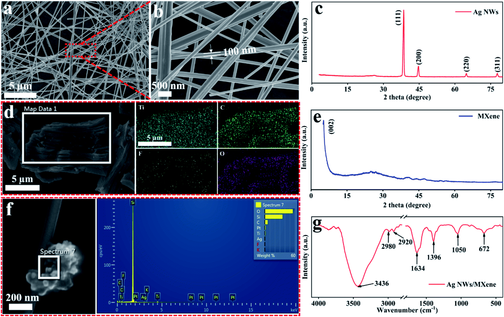 | ||
| Fig. 1 SEM images of Ag NWs (a and b); XRD pattern of Ag NWs (c); SEM and corresponding element mappings of multi-layered MXene (d); XRD pattern of few-layered MXene (e); SEM image and infrared spectrum of the composite electrode material (f and g). | ||
A capacitive pressure sensor was fabricated using a natural bamboo leaf as the dielectric layer and Ag NW/MXene composite materials as electrodes (see the Experimental section for details), with a sandwich-structure shown in Fig. 2a. To facilitate the transfer of Ag NW/MXene composite conductive materials from the filter membrane to the PDMS substrate after vacuum filtration, the mass ratio of Ag NWs to MXene sheets was controlled at 5![[thin space (1/6-em)]](https://www.rsc.org/images/entities/char_2009.gif) :1. SEM images of the composite electrode show that the Ag NWs are wrapped by the MXene sheets, producing a one-dimensional (1D) combination structure with a coarse surface (Fig. 2b and c). The fabricated rough composite electrode is favourable for yielding more contact points with the dielectric layer during the loading process, thereby improving the sensor performance.38
:1. SEM images of the composite electrode show that the Ag NWs are wrapped by the MXene sheets, producing a one-dimensional (1D) combination structure with a coarse surface (Fig. 2b and c). The fabricated rough composite electrode is favourable for yielding more contact points with the dielectric layer during the loading process, thereby improving the sensor performance.38
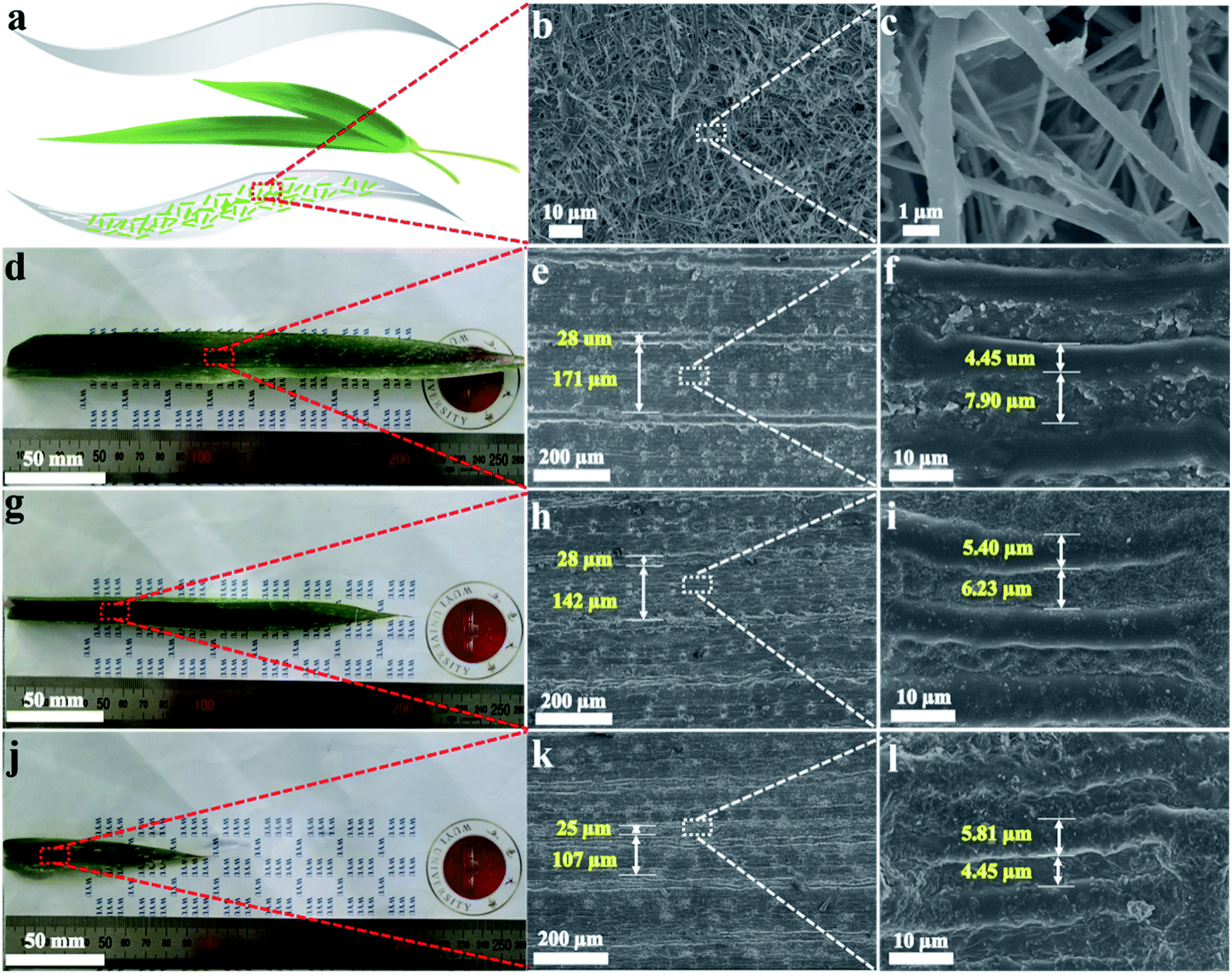 | ||
| Fig. 2 Structure diagram of the flexible capacitance sensor (a); SEM images of the Ag NW/MXene composite electrode with different scales (b and c); real photographs and corresponding SEM images of natural bamboo leaves at senile (d–f), mature (g–i), and infantile stages (j–l), the diameter ratios of the bulge to the groove within the hierarchical microstructure are about 1:6, 1:5, and 1:4 in a large scale, and 3:5, 4:5, and 6:5 in a small scale. | ||
To evaluate the effect of the microstructure scale of dielectrics on the sensor performance, the bamboo leaf at different growth stages was used as the dielectric layer of the capacitive sensor (Fig. 2d, g, and j). SEM images with a scale-bar of 200 μm display that the bulges and grooves are regularly and straight distributed on the leaf surface (Fig. 2e, h, and k). The average diameters of the convex/concave parts were 28/171 μm, 28/142 μm, and 25/107 μm, which corresponded to the leaves at senile, mature, and infantile stages, respectively, suggesting that the width of the adjacent bulges gradually increases as the leaf matures. It is worth noting that a sub-microstructure with similar morphology was observed under a scale-bar of 10 μm when the groove regions were magnified (Fig. 2f, i, and l). The average diameters of the convex/concave parts decreased accordingly, exhibiting the values of 4.45/7.90, 5.40/6.23, and 5.81/4.45 μm for the leaves at different growth stages. Therefore, the results denote the natural bamboo leaves render a hierarchical structure with similar morphology, as well as different sizes determined by the mature degree.
2.2 Performance and working principle of capacitive pressure sensors
The sensing performance of flexible capacitive sensors with the hierarchical microstructure was further characterized. The pressure sensors using the bamboo leaves at the infantile, mature, and senile stages were named i-sensor, m-sensor, and s-sensor, respectively. Sensitivity (S) of the capacitive sensor relies on the slope of the capacitance change versus the applied pressure curve, expressed by the equation: S = δ(ΔC/C0)/δP (where C and C0 refer to the capacitance at the loading and initial states, ΔC is the variation of capacitance (C − C0), P represents the applied pressure).41,42 The comparison of the three pressure sensors' relative capacitance changes was provided in Fig. 3a. As expected, the sensitivity of the micro-structured sensors is adjustable, hinging on the size of the hierarchical microstructure. There are three distinct sensitivity ranges within 0–600 kPa for the sensors. The highest sensitivity of 2.08 kPa−1 was achieved for the m-sensor within the initial small pressure range of 0–1 kPa, which was 1.41 and 9.04 times higher than that of the s-sensor and the i-sensor, respectively. In the second range of 1–100 kPa, the sensitivity of the i-sensor, m-sensor, and s-sensor reduced to 0.06, 0.08, and 0.16 kPa−1, respectively. Moreover, the m-sensor and s-sensor still had a significant sensing capability (S = 0.01 kPa−1) within the third high-loading range of 100–600 kPa. Table 1 is a summary of the maximum sensitivity and the detectable pressure range of the hierarchical-micro-structured sensor, compared with those of the capacitive pressure sensor based on the dielectric layer with a natural or replicated microstructure (natural or dried rose petal,37,43 PDMS with lotus leaf/micropillar array/porous air gap structure,15,20,36,38 and Ecoflex with a cube sugar structure18) in previous literature. Notably, our device simultaneously exhibited the highest sensitivity and a considerably wide detection range.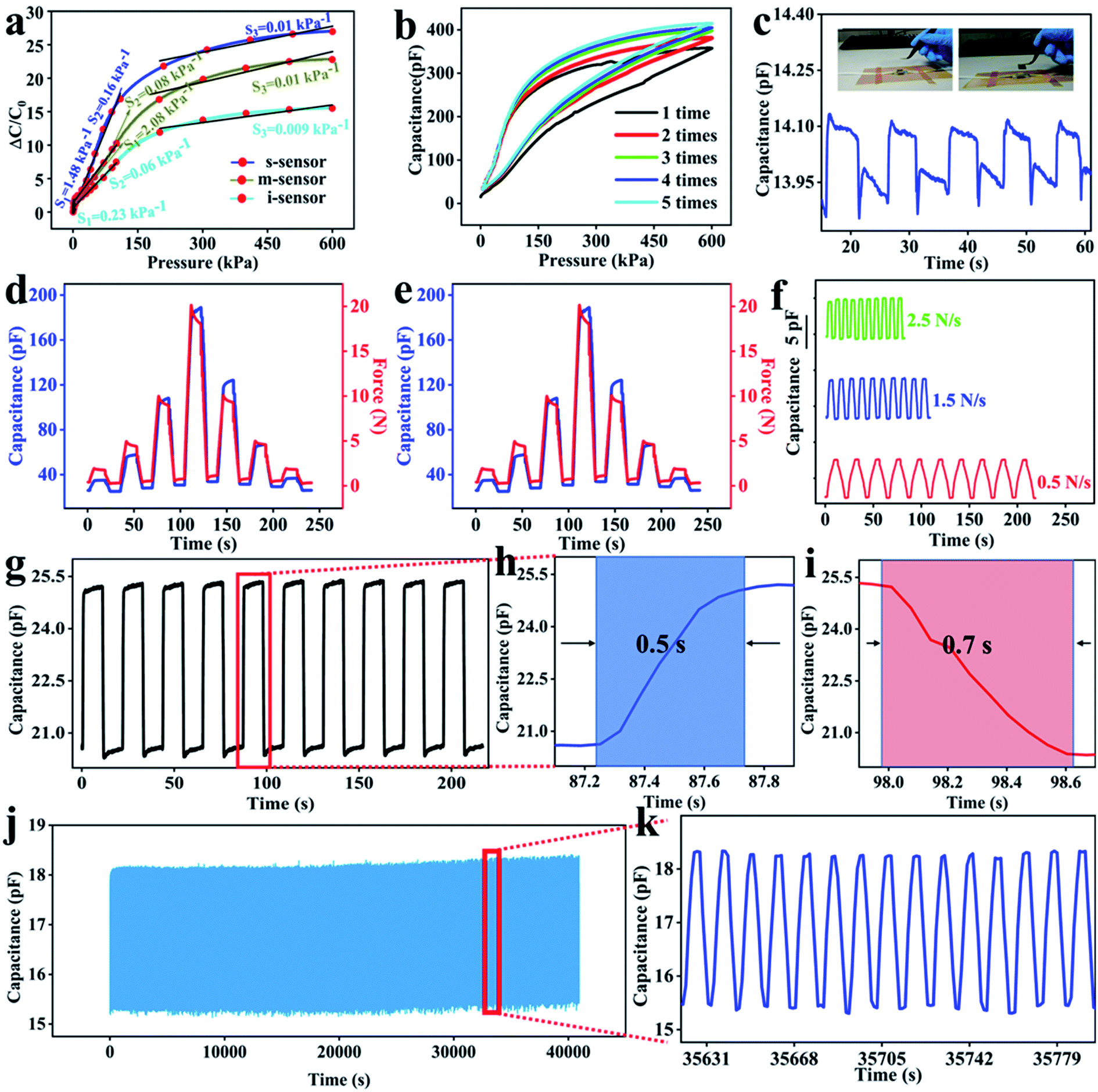 | ||
| Fig. 3 Performance analysis of flexible pressure sensors based on bamboo leaves-dielectric layers. (a) Capacitance changes-loading curves of hierarchical micro-structured sensors; (b) hysteresis curves of the sensor for the first five cycles within a response range of 0–600 kPa; (c) test of the sensor's capability of detecting a lightweight object by loading/unloading a piece of iron sheet with a weight of 0.2 g; (d) capacitance responses under the stepped loading/unloading forces of 2, 5, 10, and 20 N; cyclic capacitance responses under the loading forces of 2, 4, and 10 N (e), as well as those at loading speeds of 0.5, 1.5, and 2.5 N s−1 (f); (g) time-resolved capacitive response of the sensor under 1 N; dynamic response (h) and relaxation time (i) of the sensor for a single cycle; (j) stability test of the device under 5 N for 4000 cycles; (k) magnified curves of (j) at the later cycle stage. | ||
| Dielectric layer | Sensitivity max. | Detection range | Ref. |
|---|---|---|---|
| Nylon net | 0.33 kPa−1 (<1 kPa) | 1–5 kPa (0.007 kPa−1) | 43 |
| Rose petal | 0.08 kPa−1 (<5 kPa) | ∼60 kPa | 37 |
| Dried rose petal | 1.54 kPa−1 (<1 kPa) | 1–40 kPa (0.068 kPa−1) | 36 |
| 40–115 kPa (0.014 kPa−1) | |||
| PDMS with lotus leaf structure | 1.194 kPa−1 (<2 kPa) | 2–15 kPa (0.077 kPa−1) | 38 |
| PDMS with micropillar array structure | 0.42 kPa−1 (<1.5 kPa) | 1.5–13 kPa (0.04 kPa−1) | 15 |
| PDMS with high porosity and air gaps | 1.15 kPa−1 (<1 kPa) | 1–400 kPa (0.02 kPa−1) | 20 |
| 400–1000 kPa (0.004 kPa−1) | |||
| Porous Ecoflex with a cube sugar structure | 0.601 kPa−1 (<5 kPa) | 5–130 kPa (0.077 kPa−1) | 18 |
| Bamboo leaf (m-sensor) | 2.08 kPa−1 (<1 kPa) | 1–100 kPa (0.08 kPa−1) | This work |
| 100–600 kPa (0.01 kPa−1) | |||
| Bamboo leaf (s-sensor) | 1.48 kPa−1 (<1 kPa) | 1–100 kPa (0.16 kPa−1) | This work |
| 100–600 kPa (0.01 kPa−1) |
Other sensing properties were investigated by taking the m-sensor as an example (Fig. 3b–k). The hysteresis behaviour of the sensor was analysed by loading/unloading pressures on the device for the first five cycles within 0–600 kPa (Fig. 3b). From the second cycle, the hysteresis loop began to change a little, revealing good recoverability of the capacitive sensor within a wide pressure range. Then the device's capability of detecting a lightweight object was evaluated by repeatedly loading/unloading a piece of iron sheet with a weight of 0.2 g (∼20 Pa) (Fig. 3c). The regular and stable curve reflects that the sensor can reliably respond to a small weight through the capacitance signals. To test the dynamic stability of the micro-structured sensor, a single response to a step-increased and decreased force of 2, 5, 10, and 20 N, and the cyclic responses to a gradient force of 2, 4, and 10 N (Fig. 3d and e) were monitored. The sensor capacitance increased as the external force was elevated, and the capacitance profile exhibited an excellent match with the force input, reflecting that the sensor possesses outstanding stability and good pressure recognition. In addition, the sensor showed a rapid change and good recovery in its capacitance at different loading/unloading speeds of 0.5, 1.5, and 2.5 N s−1 with a constant force of 2.5 N (Fig. 3f), demonstrating favourable reversibility of the sensor. The response time of the pressure sensor was studied by detecting ten cycles under 1 N (Fig. 3g). During the cycling, the device capacitance abruptly changed. A typical cycle curve is amplified in Fig. 3h and i, which display that the response and relaxation time of the sensor are 0.5 and 0.7 s, respectively. However, the measurement of the response time is restricted by the movement rate of the push–pull machine (2.5 N s−1) and the data acquisition rate of the LCR meter (30 data per s). Thus, the actual response time of the sensor was even shorter than what had been measured.10 Compared with the response time, the hysteresis during the unloading process was small, leading to a relatively longer relaxation time. The result is consistent with that shown in Fig. 3b. To assess the mechanical reliability and robustness of the device, the cyclic tests were conducted by dynamically loading/unloading a constant force of 5 N for over 4000 cycles (10 s for each cycle) (Fig. 3j). The response curve for the 10 cycles at the later cyclic stage is shown in Fig. 3k. The negligible capacitance variation during the cycling process denotes the high stability, repeatability, and durability of the sensor.
To understand the working principle of the hierarchical micro-structured sensors, the device models were established by finite element analysis (FEA) to analyse the changes in the stress and deformation under different external pressures (see Experimental section for details). In addition, the comparison was conducted by simulating the capacitance pressure sensor based on a flat dielectric layer (Fig. 4a and b). According to the real scale ratio of the hierarchical microstructure, the diameter ratios of the bulge to the groove were set as 1:6, 1:5, and 1:4 in a large scale, and 3:5, 4:5, and 6:5 in a small scale, corresponding to the s-sensor, m-sensor, and i-sensor, respectively. As the applied pressure increased from 50 to 600 kPa, the generated stress within the sensor was accordingly elevated. Under the same pressure, the sensors possessed different stress distributions, which demonstrates strong dependence on the size of the hierarchical microstructure (Fig. 4a). The microstructure of the sensor dielectric produced the air gap between the electrode and dielectric layer. When the pressure was exerted on the sensor, the air gap volume decreased, and the stress preferentially accumulated at the contact point between the electrode material and the micro-structured bulge. Thus, the highest stress was concentrated in the s-sensor due to the largest air gap. However, the flat sensor without the air gap exhibited high resistance to the external pressure, resulting in low structural compressibility (Fig. 4b). Furthermore, we simulated the change in the displacement between the two electrodes under various loads for the flat and micro-structured sensors. Under a certain pressure, the largest displacement change was achieved by the s-sensor because of its largest stress and highest structural compression (Fig. 4c).
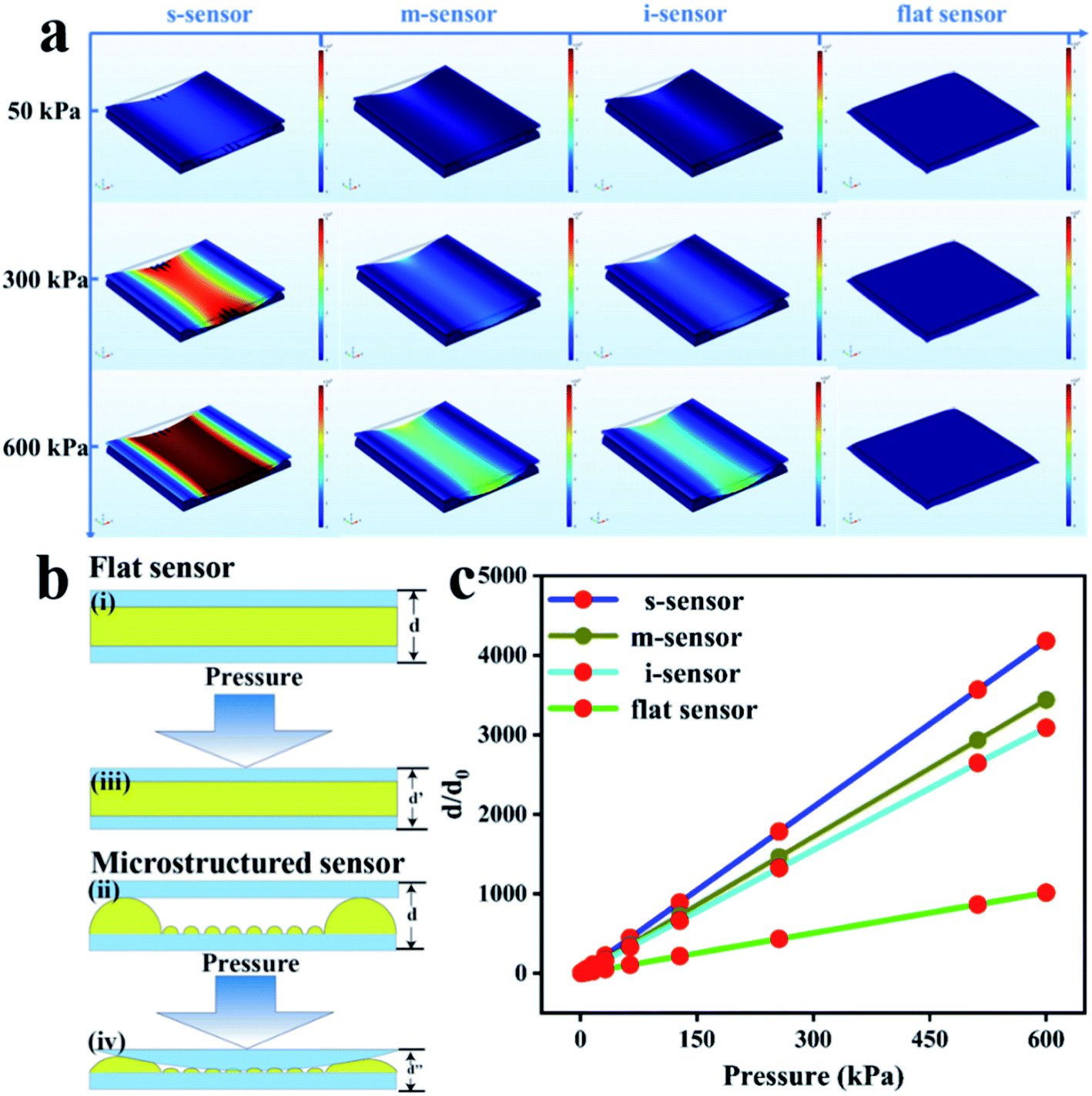 | ||
| Fig. 4 (a) Comparison of the stress distributions of the s-sensor, m-sensor, i-sensor, and flat sensor; (b) schematic diagram of the distance and contact area changes under a given load for the micro-structured and flat sensors; (c) compression displacements as the applied pressures for the s-sensor, m-sensor, i-sensor, and flat sensor. | ||
Additionally, the working principle of the capacitive sensor based on the bamboo leaf was used to explain the reasons for its high sensitivity and wide detection range. In general, the high sensitivity of a sensor originates from a large capacitance change under a given pressure. In accordance with the capacitance definition of a parallel plate capacitor (C = εS/4πkd, where ε corresponds to the dielectric constant, d represents the distance between the two plates, k is the electrostatic constant, and S refers to the effective area of the capacitor plate),44 the structural parameters (ε, d, and S) can be altered to realise a notable change in the capacitance during the loading/unloading process, and then improve the sensor sensitivity. In the hierarchical micro-structured sensor, the increasing stress compels the elastic electrode to contact with the micro-structured bulges during the loading process. As a result, the remarkable increase in the capacitance is realised due to an increase in the contact area between the electrode and dielectric layer and a decrease in the distance of the air gap. Furthermore, the large deformation makes the effective dielectric constant (ε) increase accordingly because of the permeation of the elastomer PDMS into the air gap. Hence, a notable capacitance change is received under a certain pressure, thereby endowing the sensor with high sensitivity. Moreover, our sensors can maintain a considerable sensing capability within a wide pressure range owing to a continuous contact of the electrode with the large- and small-scale microstructure of the bamboo leaf.
2.3 Applications as strain and proximity sensors
To demonstrate the practical applications of the micro-structured device as a strain and proximity sensor, its capabilities of detecting the actual object load, human physical stimuli, and proximity distance were investigated. The sensor's detection of an object loading was evaluated by repeatedly placing and removing a standard weight of 10 g. The distinguishable and steady capacitance changes were acquired, and the signal output exhibited a fixed maximum of capacitance, reflecting a highly stable response of the sensor (Fig. 5a). To verify the high speed in response to dynamic pressures, the finger and spanner quickly tapped at the device (Fig. 5b and c). The capacitance signals synchronously changed as the tap proceeded, revealing excellent repeatability and rapid response of the sensor.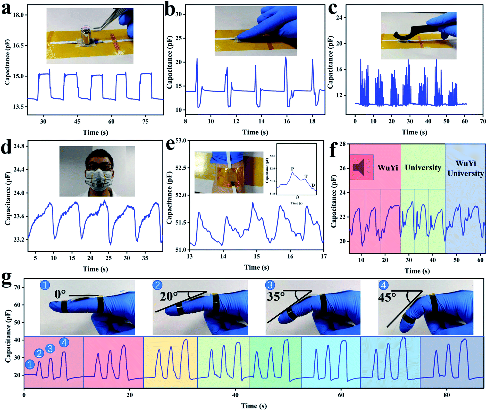 | ||
| Fig. 5 Applications as a strain sensor. Real-time capacitance changes of the sensor in response to the press of weight (a), finger (b), and spanner (c); detecting human physiological signals from the breath (d), wrist pulse (e), and speech (f); capacitance changes of the index finger bending with various angles of 0°, 20°, 35°, and 45° (g). | ||
For the convenient detection of human physiological signals, the pressure sensor was adhered to the mask, wrist, and throat of a volunteer to monitor its real-time responses to the breath, wrist pulse, and pronunciation of the volunteer (Fig. 5d–f). The respiratory rate that provides important biological signals for the physiological condition of the human body was detected by fixing the pressure sensor on a mask. When the volunteer exhaled, the air pressure pushed the sensor to compress, yielding an increase in capacitance. When the volunteer inhaled, the air pressure on the sensor was removed, and thus the sensor capacitance gradually decreased and finally recovered to its original value (Fig. 5d). The radial artery pressure is another significant indicator of the clinical diagnosis. Thus, the sensor was used to monitor the real-time wrist. The typical pulse waveform indicated the pulse at a frequency of 75 beats per min with the repeatable pattern shape, suggesting a healthy state of the volunteer (Fig. 5e). The inset in Fig. 5e presents a zoom-in pattern of the single pulse, revealing the three characteristic peaks of the arterial waveform, including the percussion wave (P wave) and the tidal wave (T wave) related to the typical radial artery pulse vibration, as well as the diastolic wave (D wave) corresponding to the late systolic artery pulse vibration.18,19 In addition, the vocalisation recognition was evaluated by attaching the sensor to the volunteer's throat. The vibration of Adam's apple from the pronunciation can bring pressure to the sensor to change the output of capacitance signals.28 When the volunteer spoke the words ‘Wuyi’ and ‘University’ three times and the phrase ‘Wuyi University’ once, the distinct capacitance changes and different patterns of signals were observed (Fig. 5f). Notably, the signals kept the repeated waveform outputs when the volunteer spoke the same word. Moreover, the waveform was quite sensitive to the frequency and volume of the speech. The above results denote that the micro-structured sensor offers excellent potential for disease diagnosis and real-time vocal recognition.
To monitor the joint movement of the human body, the sensor was attached to the index finger to detect the capacitance changes in response to the joint bending at various angles of 0°, 20°, 35°, and 45°. The capacitance increased with a rise of the bending angle and returned to the original value when the joint recovered to a relaxed state. Bending the index finger from 0° to 45° for eight cycles demonstrated a stable change in the output waveform, which confirms that the flexible capacitive sensor based on the hierarchical microstructure can accurately identify the joint bending angles (Fig. 5g).
Besides the capabilities of detecting the object load and human activities, the micro-structured device is capable of discerning the approaching distance of the human body as a proximity sensor. The volunteer was asked to suspend a palm periodically on the top of the sensor and removed it by maintaining various distances of 1, 2, 3, and 4 cm (Fig. 6a–d). As the palm approached the device, the capacitance gradually decreased. In other words, the capacitance increased with a decrease in the detection distance between the palm and the sensor. The largest capacitance change was obtained when the detection distance reached a minimum of 1 cm. During the proximity detection process, the system consisting of the human body, the air layer, and the conductive film of the sensor was regarded as a typical organic film field-effect transistor. When the human body approached the conductive film, the interface charges of the sensor were re-distributed, resulting in the capacitance change.45
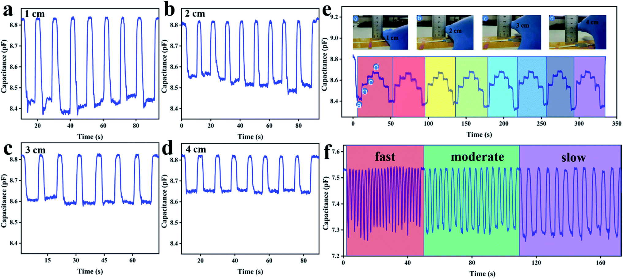 | ||
| Fig. 6 Application as a proximity sensor. Capacitance responses when a palm repeatedly approached and removed from the sensor with a distance between the palm and the sensor of 1 cm (a), 2 cm (b), 3 cm (c), and 4 cm (d); cyclic tests of the capacitance changes with the stepped distances of 1–4 cm (e) and at different approach/departure speeds (f); the insets of (e) are photographs of the approaching process. | ||
To evaluate the reliability of the distance detection, the step distance between the palm and the sensor was cyclically kept at 1, 2, 3, and 4 cm. The output signals showed high repeatability and stability, proving that our sensor can reliably identify the approaching distance (Fig. 6e). In addition, the capacitance could rapidly respond to the approaching distance regardless of the moving speed (Fig. 6f). Thus, the micro-structured device is quite useful in some application scenarios where the measurement of a close distance is required, such as safety pre-warning, human-computer interaction, and health monitoring.
3 Conclusion
To sum up, a simple sandwiched pressure sensor based on the Ag NW/MXene composite electrode and the bamboo-leaf dielectric layer with a hierarchical structure was developed in this experiment. By choosing the appropriate size of the bamboo leaf microstructure, the capacitive sensor was endowed with high sensitivity of 2.08 kPa−1 within a low-pressure range, a broad detection range up to 600 kPa, and excellent mechanical stability over 4000 cycles. The designed sensor could reliably detect a lightweight object load and the external force of repeated real-time taps. Furthermore, the applications of a strain sensor to the respiratory rate and wrist pulse monitoring, vocal recognition, and joint movement were demonstrated, and the detection of the approaching distance by a proximity sensor was proven. It is expected that the micro-structured sensor is an applicable candidate for wearable devices, human-computer interfaces, disease diagnosis, and pre-warning.4 Experimental section
4.1 Construction of flexible strain and proximity sensors
Ag NWs were synthesised via a hydrothermal method, as described in the previous work.46 MXene sheets were obtained from the layer-structured Ti3AlC2, which was prepared by selectively etching Al of MAX phase precursor powder (11 Technology Co., Ltd., China). Initially, 1.6 g of LiF was dissolved in 9 M of HCl, and then 1 g of Ti3AlC2 powder was introduced into the above mixture through magnetic stirring. After the etching reaction at 35 °C for 48 h, the resulting solution was repeatedly centrifuged at 3500 rpm and washed with deionised water until the supernatant pH value was approximately 6. Finally, the obtained precipitate was further ultrasonic-processed in an ice bath under the Ar atmosphere for 2 h to achieve fewer-layered MXene sheets. The composite conductive materials were prepared by mixing the Ag NWs and MXene sheets with a weight ratio of 5:1.
The sensor electrode was fabricated by coating and transferring the composite onto the PDMS (Sylgard 184, Dow Corning) substrate via a vacuum-filtration process. The bamboo leaves (the main chemical components include flavonoids, active polysaccharides, special amino acids and their derivatives47) at different growth stages were repeatedly rinsed with deionised water, and the absorbent cotton was used to remove the excess water carefully. The clean and dry leaves were cut into 10 mm × 10 mm in area as the dielectric layers. Subsequently, the flexible capacitive pressure sensor was integrated through the natural dielectric layer sandwiched by the two Ag NW/MXene composite electrodes.
4.2 Finite element analysis (FEA) simulation of natural plant structures
FEA was conducted to simulate the natural bamboo structure at different growth stages utilising the commercial package COMSOL5.4. The simulation models of the bamboo leaves were established according to the proportion of their real sizes. All the bamboo leaves displayed the hierarchical microstructure consisting of the regular bulges and grooves in two scales. In a large scale, the diameter ratio of the bulge to the channel was set as 1:6, 1:5, and 1:4 corresponding to the s-sensor, m-sensor, and i-sensor, respectively. In a small scale, the ratios were controlled at 3:5, 4:5, and 6:5. To evaluate the advantage of the hierarchical microstructure, the capacitive sensors based on the planar and micro-structured dielectric layers were compared to analyse the stress-distribution and deformation-displacement under various pressures. The surface morphology of the electrodes was ignored, and metal plates were used.
4.3 Characterization
The morphology of the dielectric layers and electrode materials were characterized using a field emission scanning electron microscope (FE-SEM, Zeiss Sigma 500, Germany). The composition of conductive material was evaluated utilising an X-ray diffractometer (XRD, X'pert Pro MFD, Panalytical, The Netherlands) with a Cu Kα radiation (λ = 1.54178 Å). A push–pull force gauge (LE, LiShi, China) was used to subject stresses on the sensors. The response performance of stress-dependent sensor was performed by monitoring the capacitance variations of the device in real-time utilizing an LCR (Inductance, Capacitance, Resistance) measurement instrument (IM3526, Rizhi, Japan) at the frequency of 1 MHz.Conflicts of interest
There are no conflicts to declare.Acknowledgements
This work was supported by the Natural Science Foundation of Guangdong Province (2021A1515010691); Major Program of Basic Research and Applied Research of Guangdong Province (2019KZDXM051); Wuyi University-Hong Kong-Macau Joint Research and Development Fund (2019WGALH06); Laboratory of Optoelectronic Materials and Applications (Department of Education of Guangdong Province) (2017KSYS011); College Students Maker Space Project of Wuyi University (2020CX07); Special Fund for Scientific and Technological Innovation Cultivation of University Students in Guangdong Province (pdjh2020b0610).References
- X. Wang, L. Dong, H. Zhang, R. Yu, C. Pan and Z. L. Wang, Adv. Sci., 2015, 2, 1500169 CrossRef PubMed.
- J. C. Yang, J. Mun, S. Y. Kwon, S. Park, Z. Bao and S. Park, Adv. Mater., 2019, 31, e1904765 CrossRef PubMed.
- Q. J. Sun, X. H. Zhao, C. C. Yeung, Q. Tian, K. W. Kong, W. Wu, S. Venkatesh, W. J. Li and V. A. L. Roy, ACS Appl. Mater. Interfaces, 2020, 12, 37239–37247 CrossRef CAS PubMed.
- Y. Guo, M. Zhong, Z. Fang, P. Wan and G. Yu, Nano Lett., 2019, 19, 1143–1150 CrossRef PubMed.
- X. Zeng, Z. Wang, H. Zhang, W. Yang, L. Xiang, Z. Zhao, L. M. Peng and Y. Hu, ACS Appl. Mater. Interfaces, 2019, 11, 21218–21226 CrossRef CAS PubMed.
- E. S. Hosseini, L. Manjakkal, D. Shakthivel and R. Dahiya, ACS Appl. Mater. Interfaces, 2020, 12, 9008–9016 CrossRef CAS PubMed.
- H. Yao, T. Sun, J. S. Chiam, M. Tan, K. Y. Ho, Z. Liu and B. C. K. Tee, Adv. Funct. Mater., 2021, 2008650 CrossRef.
- K. Xu, Y. Lu and K. Takei, Adv. Mater. Technol., 2019, 4, 1800628 CrossRef.
- X. Wang, Y. Gu, Z. Xiong, Z. Cui and T. Zhang, Adv. Mater., 2014, 26, 1336–1342 CrossRef CAS PubMed.
- S. Zhao, W. Ran, D. Wang, R. Yin, Y. Yan, K. Jiang, Z. Lou and G. Shen, ACS Appl. Mater. Interfaces, 2020, 12, 32023–32030 CrossRef CAS PubMed.
- G. J. Zhu, P. G. Ren, J. Wang, Q. Duan, F. Ren, W. M. Xia and D. X. Yan, ACS Appl. Mater. Interfaces, 2020, 12, 19988–19999 CrossRef CAS PubMed.
- P. Zhao, R. Zhang, Y. Tong, X. Zhao, Q. Tang and Y. Liu, Adv. Electron. Mater., 2020, 6, 1901426 CrossRef CAS.
- K. Xia, C. Wang, M. Jian, Q. Wang and Y. Zhang, Nano Res., 2017, 11, 1124–1134 CrossRef.
- G. Y. Bae, S. W. Pak, D. Kim, G. Lee, H. Kim do, Y. Chung and K. Cho, Adv. Mater., 2016, 28, 5300–5306 CrossRef CAS PubMed.
- Y. Luo, J. Shao, S. Chen, X. Chen, H. Tian, X. Li, L. Wang, D. Wang and B. Lu, ACS Appl. Mater. Interfaces, 2019, 11, 17796–17803 CrossRef CAS PubMed.
- S. Pyo, J. Choi and J. Kim, Adv. Electron. Mater., 2018, 4, 1700427 CrossRef.
- S. Chen, B. Zhuo and X. Guo, ACS Appl. Mater. Interfaces, 2016, 8, 20364–20370 CrossRef CAS PubMed.
- D. Kwon, T. I. Lee, J. Shim, S. Ryu, M. S. Kim, S. Kim, T. S. Kim and I. Park, ACS Appl. Mater. Interfaces, 2016, 8, 16922–16931 CrossRef CAS PubMed.
- J. C. Yang, J. O. Kim, J. Oh, S. Y. Kwon, J. Y. Sim, D. W. Kim, H. B. Choi and S. Park, ACS Appl. Mater. Interfaces, 2019, 11, 19472–19480 CrossRef CAS PubMed.
- W. Li, X. Jin, Y. Zheng, X. Chang, W. Wang, T. Lin, F. Zheng, O. Onyilagha and Z. Zhu, J. Mater. Chem. C, 2020, 8, 11468–11476 RSC.
- Y. Kim, S. Jang and J. H. Oh, Microelectron. Eng., 2019, 215, 111002 CrossRef.
- P. Wei, X. Guo, X. Qiu and D. Yu, Nanotechnol, 2019, 30, 455501 CrossRef CAS PubMed.
- S. Kang, J. Lee, S. Lee, S. Kim, J.-K. Kim, H. Algadi, S. Al-Sayari, D.-E. Kim, D. Kim and T. Lee, Adv. Electron. Mater., 2016, 2, 1600356 CrossRef.
- J. Yang, D. Tang, J. Ao, T. Ghosh, T. V. Neumann, D. Zhang, E. Piskarev, T. Yu, V. K. Truong, K. Xie, Y. C. Lai, Y. Li and M. D. Dickey, Adv. Funct. Mater., 2020, 30, 2002611 CrossRef CAS.
- B. Ji, Q. Zhou, J. Wu, Y. Gao, W. Wen and B. Zhou, ACS Appl. Mater. Interfaces, 2020, 12, 31021–31035 CrossRef CAS PubMed.
- J. Yang, S. Luo, X. Zhou, J. Li, J. Fu, W. Yang and D. Wei, ACS Appl. Mater. Interfaces, 2019, 11, 14997–15006 CrossRef CAS PubMed.
- L. Ma, X. Shuai, Y. Hu, X. Liang, P. Zhu, R. Sun and C.-p. Wong, J. Mater. Chem. C, 2018, 6, 13232–13240 RSC.
- Q. Zhou, B. Ji, Y. Wei, B. Hu, Y. Gao, Q. Xu, J. Zhou and B. Zhou, J. Mater. Chem. A, 2019, 7, 27334–27346 RSC.
- K. Wang, Z. Lou, L. Wang, L. Zhao, S. Zhao, D. Wang, W. Han, K. Jiang and G. Shen, ACS Nano, 2019, 13, 9139–9147 CrossRef CAS PubMed.
- X. Zhou, Y. Zhang, J. Yang, J. Li, S. Luo and D. Wei, Nanomater, 2019, 9, 496 CrossRef CAS PubMed.
- Y. Q. Liu, J. R. Zhang, D. D. Han, Y. L. Zhang and H. B. Sun, ACS Appl. Mater. Interfaces, 2019, 11, 38084–38091 CrossRef CAS PubMed.
- Y. Xiong, Y. Shen, L. Tian, Y. Hu, P. Zhu, R. Sun and C.-P. Wong, Nano Energy, 2020, 70, 104436 CrossRef CAS.
- Y. Gao, G. Yu, J. Tan and F. Xuan, Sens. Actuators, A, 2018, 280, 205–209 CrossRef CAS.
- J. Shin, B. Jeong, J. Kim, V. B. Nam, Y. Yoon, J. Jung, S. Hong, H. Lee, H. Eom, J. Yeo, J. Choi, D. Lee and S. H. Ko, Adv. Mater., 2020, 32, e1905527 CrossRef PubMed.
- P. S. Das, A. Chhetry, P. Maharjan, M. S. Rasel and J. Y. Park, Nano Res., 2019, 12, 1789–1795 CrossRef CAS.
- Y. Wan, Z. Qiu, J. Huang, J. Yang, Q. Wang, P. Lu, J. Yang, J. Zhang, S. Huang, Z. Wu and C. F. Guo, Small, 2018, 14, e1801657 CrossRef PubMed.
- A. Elsayes, V. Sharma, K. Yiannacou, A. Koivikko, A. Rasheed and V. Sariola, Adv. Sustainable Syst., 2020, 4, 2000056 CrossRef CAS.
- Y. Wan, Z. Qiu, Y. Hong, Y. Wang, J. Zhang, Q. Liu, Z. Wu and C. F. Guo, Adv. Electron. Mater., 2018, 4, 1700586 CrossRef.
- X. Shi, H. Wang, X. Xie, Q. Xue, J. Zhang, S. Kang, C. Wang, J. Liang and Y. Chen, ACS Nano, 2019, 13, 649–659 CrossRef CAS PubMed.
- D. Kim, T. Y. Ko, H. Kim, G. H. Lee, S. Cho and C. M. Koo, ACS Nano, 2019, 13, 13818–13828 CrossRef CAS PubMed.
- J. Hwang, S. G. Lee, S. Kim, J. S. Kim, D. H. Kim and W. H. Lee, ACS Appl. Polym. Mater., 2020, 2, 2190–2198 CrossRef CAS.
- J. Choi, D. Kwon, K. Kim, J. Park, D. D. Orbe, J. Gu, J. Ahn, I. Cho, Y. Jeong, Y. Oh and I. Park, ACS Appl. Mater. Interfaces, 2020, 12, 1698–1706 CrossRef CAS PubMed.
- Z. He, W. Chen, B. Liang, C. Liu, L. Yang, D. Lu, Z. Mo, H. Zhu, Z. Tang and X. Gui, ACS Appl. Mater. Interfaces, 2018, 10, 12816–12823 CrossRef CAS PubMed.
- B. C. K. Tee, A. Chortos, R. R. Dunn, G. Schwartz, E. Eason and Z. Bao, Adv. Funct. Mater., 2014, 24, 5427–5434 CrossRef CAS.
- Y. Du, G. Yu, X. Dai, X. Wang, B. Yao and J. Kong, ACS Appl. Mater. Interfaces, 2020, 12, 51987–51998 CrossRef CAS PubMed.
- X. He, R. He, A. l. Liu, X. Chen, Z. Zhao, S. Feng, N. Chen and M. Zhang, J. Mater. Chem. C, 2014, 2, 9737–9745 RSC.
- G. K. Mahunu, H. Zhang, M. T. Apaliya, Q. Yang, X. Zhang and L. Zhao, Postharvest Biol. Technol., 2018, 141, 1–7 CrossRef CAS.
| This journal is © The Royal Society of Chemistry 2021 |