
 Open Access Article
 This Open Access Article is licensed under a Creative Commons Attribution-Non Commercial 3.0 Unported Licence
Engineered nano-sphere array of gold-DNA core–shells and junctions as opto-plasmonic sensors for biodetection
Nahid Osanlooa,
Vahid Ahmadi *b,
Mohammad Naser-Moghaddasia and
Elham Darabic
*b,
Mohammad Naser-Moghaddasia and
Elham Darabic
aFaculty of Engineering, Science and Research Branch, Islamic Azad University, Tehran, Iran
bDepartment of Electrical and Computer Engineering, Tarbiat Modares University, Tehran, Iran. E-mail: v_ahmadi@modares.ac.ir
cPlasma Physics Research Center, Science and Research Branch, Islamic Azad University, Tehran, Iran
First published on 9th August 2021
Abstract
In this paper, we design opto-plasmonic sensors by the engineered arrangement of gold-nanospheres. We use DNA-gold nanoparticle (GNP) core–shells and DNA rods as junctions between GNPs with a fishnet ground layer for controlling and improving the absorbance and reflection in the range of 100–300 THz. Based on available data, we check the effects of healthy and cancerous cells on the reflection parameter. Here, we demonstrate how the DNA junctions and distance between the nanospheres can be considered to modify the reflection. These structures can be utilized as opto-plasmonic sensors with high sensitivity to distinguish materials in terms of refractive indices. We can use an array of these sensors for both spectroscopy and optical imaging on a real scale. The proposed structures with different topologies are analyzed and their figure of merits (FOM) and sensitivities are obtained. The structure based on the DNA rods as junctions between GNPs shows the best FOM value of 340 RIU−1 and the core–shell heptamer structure has the best sensitivity of about 1287 nm RIU−1.
Introduction
The metamaterial is known for its particular characteristics and structure, which cannot be found in nature, and has been designed artificially.1,2 This extraordinary behavior of the metamaterial has been considered for manipulating the electromagnetic wave (EM) in the optical regime3 considering the surface plasmon (SP)4 and localized surface plasmon resonance (LSPR).5 The optical metamaterials are used for various goals such as bending6 or absorbing the electromagnetic wave,7 which is essential for a perfect broadband absorber8 or optical cloak design.9 The nanoparticles array was studied for the invisibility10 of an object by modifying the permittivity and controlling the EM field using the optic transformer.11 The optic transformer is considered for determining the effective permittivity of each layer of the optical cloak.12Moreover, the plasmonic behavior of nanoparticles is essential for designing a cloak layer.13,14
The plasmonic characteristic has also been considered for various optical devices, such as nanoantenna15,16 and optical absorber for spectroscopy applications.17
Nowadays, the nanoantennas and nanoabsorber have been developed with various shapes, such as monopole,18 dipole,19 and bowtie,20 for single resonances. On the other hand, more complicated models have been studied for a multi-band and Fano shape, such as ring/disk plasmonic nanocavities21 and heptamer clusters composed of split nanorings.22 In addition, these nanoabsorbers have been considered as a part of an optical sensor for spectroscopy applications23 and other applications, such as solar cells for energy-harvesting.24
Recently, various research studies have been done on designing optical devices that are used for the detection of materials based on frequency shift or other parameters, such as reflection and absorption value.25,26
The metamaterials and metasurfaces with various formations have been developed for THz applications27 and bio-detecting.28 In these metasurfaces, the gaps provide capacitance for concentrating energy and making hotspots to increase the sensitivity of the sensors.29 The split ring resonators in different shapes and nanoapertures are the main form of metamaterials for THz and mid-infrared applications.30 Moreover, the optical absorber is known as another type of metamaterial, which has been developed for optical sensing by increasing the figure of merit as a perfect absorber.31
Herein, a new structure based on an engineered nano-sphere array of gold with DNA junctions as an opto-plasmonic sensor is presented for bio-detection. To improve the sensor structure, we use DNA nanorods to control the electric field inside the structure. The fabrication of DNA nanorods has already been reported.32–34 It is shown that by changing the DNA state and the distance between the arrays, the absorbance properties can be changed. In short, the proposed structure can be used for several applications, including spectroscopy and bio-optical sensors.
Optical materials definition
The plasmonic material
For noble metals (for example, gold, silver, and copper), the dielectric function at frequencies higher than the plasma frequency (ωp < ω) is:
 | (1) |
The DNA material
Organic materials, such as DNA composed of metals and polymers, are considered for controlling the resistance of electronic devices in order to create a switch.37,38 Even though the electrical conductivity of DNA is low, it can be controlled by combining DNA with metal nanoparticles (e.g., Au, Ag, Li) and creating quasi-metal structures.39 The DNA rods have less volume than the metal part (nanospheres and substrate), so the effect of the refractive index of the DNA on the response of the absorber is not impressive. The conductivity of the conventional DNA is very low, in the range of 10−12 S m−1, which is different for various types of DNA.40For example, to increase the conductivity of DNA, it is combined with Li nanoparticles.41 The ε of DNA bio-material components is in the range of 1 to 1.2.42 Therefore, in our simulation, we assume an average value of 1.1 for n and ignore its frequency dependency. Therefore, the bonding of DNA with nanoparticles of silver or gold43 and designing DNA crystals have been considered for using the reconfigurable characteristics of the DNA in the optical spectrum. According to the practical results in ref. 44, we consider that the DNA combined with metal NPs has the conductivity of 1000, which is based on a current–voltage diagram presented in ref. 38. Apparently, the ratio of the DNA to the silver or gold nanoparticle plays an important role in determining the value of the conductivity of the DNA.
Modeling of the proposed structures
The proposed structures are shown in Fig. 1(a)–(d). Here, we use a nanosphere structure that is located on a substrate of Si3N4 with a thickness of 50 nm and a refractive index of 1.74. It is placed on a fishnet form as a ground layer. The thickness of the fishnet layer is assumed to be 10 nm and the size of the apertures is 20 × 20 nm2. The reason for choosing the fishnet structure is its use on skin to detect cancer. On the other hand, it improves the operation. Moreover, the gaps in the fishnet make a new capacitance in our system, and we also have a higher effective inductance value as the electrical length of the metal is increased.45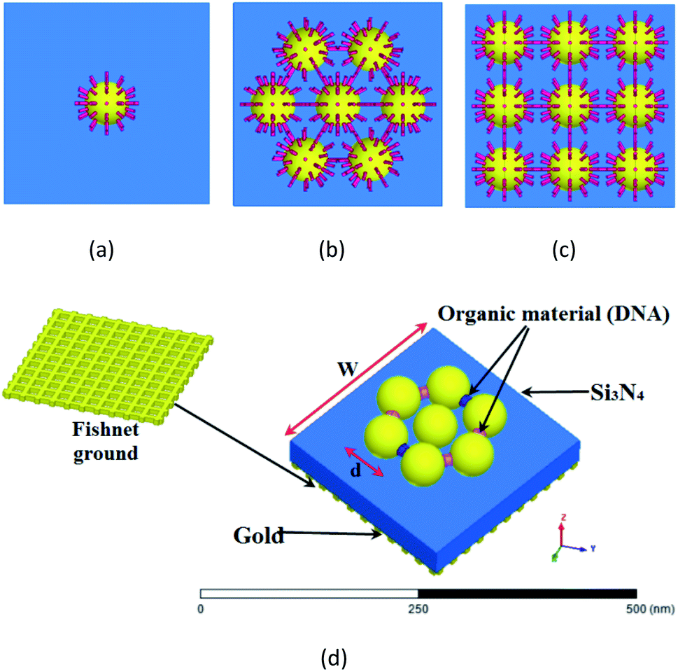 | ||
| Fig. 1 (a) Gold-DNA core–shell nanosphere structure (Type-A). (b) The heptamer gold-DNA core–shell nanospheres structure (Type-B). (c) 3 × 3 nanosphere array of the gold-DNA core–shell structure (Type-C). (d) The geometry of the proposed structure (Type-D) with gold-fishnet ground. | ||
In this paper, the CST microwave studio software is used to simulate our analysis in the time-domain. A hexahedral legacy is defined by the software, and a wave port is utilized to excite the proposed structures.
Because of the symmetrical shape of the structure, the polarization effect can be ignored. Therefore, it does not matter whether the TE or TM mode is examined, so we choose the periodic boundary conditions. We consider the X side as the perfect electric conductor (PEC), and the Y side as the perfect magnetic conductor (PMC) to provide the periodic boundary condition. We take TM polarization in the simulation.
The Palik model is used for the metal nanoparticle, which is known as a practical model, and it is available in the material library of the CST microwave studio.46 It is a tested model for nanoparticles, and will yield almost identical results with experiments. Here, we assume d = 70 nm for the diameter of the nanospheres. As shown in ref. 47 for the diameter of 60 nm, once a gold nanoparticle has the same behavior as a planar surface and for increasing the coupling between elements to provide higher absorption in this study, the diameter of the elements is assumed to be 70 nm and w = 320 nm for the total size of the unit cells.
We will study the structures based on the gold-DNA core–shell or DNA as a junction. First, as shown in Fig. 1(a), we create a nanosphere with a shell of DNA rods with lengths of 15 nm and a diameter of 5 nm. We call this structure Type-A.
In the following, we consider a more complex structure of 7 nanospheres with a shell of DNA rods to create the heptamer structure. This structure is given in Fig. 1(b), and we call it Type-B. The distance from the center of the nanosphere to the center of the other nanospheres is 100 nm, and six nanospheres are arranged with a 60° angle. The DNA rods lengths are 15 nm with a diameter of 5 nm. The height of the nanospheres from the substrate is equal to the length of the DNA rod (15 nm).
In the next step, the 3 × 3 nanosphere array of gold-DNA core–shell is presented in Fig. 1(c), and we call it Type-C.
In the last structure, we connect nanospheres with 30 nm long and 10 nm diameter rods, as shown in Fig. 1(d), and we call this structure Type-D. This structure is a kind of 2D DNA-based plasmonic crystal.33,48 The nanosphere with negative permittivity makes an inductance parallel with resistance, and two capacitances appear on two sides of the nanosphere, where the energy concentrates there. In addition, the dielectric capacitance should be taken into account in an equivalent circuit.49
Discussions and results
As shown in Fig. 1(a)–(d), our focus is on three different structures, Type-B, Type-C and Type-D. These gold-DNA plasmonic structures ultimately can be considered as a sensor element for cancer diagnosis. In this section, the reflectance and electric field distribution are considered as the two main parameters.Gold-DNA core–shell nanospheres
In this section, we study the gold-DNA core–shell nanosphere and examine the structure reflection for the three different structures of Type-A, Type-B and Type-C, as shown in Fig. 2. In Type-A, the reflection value is about −19 dB at the frequency of 290 THz. In Type-B, the reflection value is increased to −16 dB at 240 THz, and it is about −13 dB at 230 THz in Type-C. This reflection increase is originated from the losses of the metal nanosphere resistance. On the other hand, in Type-B and Type-C, with increasing number of nanospheres, the resonance frequency is red-shifted, which can be attributed to the increase of the capacitance in the structures.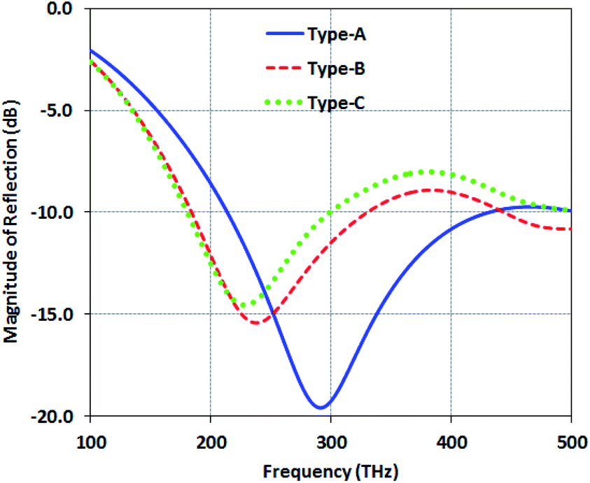 | ||
| Fig. 2 Magnitude of the reflection of structures with gold-DNA core–shell nanospheres (Type-A, Type-B and Type-C). | ||
The distribution and intensity of fields are significant to analyze the performance of each structure. The electric field distribution for Type-A is presented in Fig. 3(a). The simulation results indicate that the conductivity in the DNA rods leads to the diffusion of the field, which makes this structure qualified for optic imaging as a lens covering all over the zone uniformly. Meanwhile, the interaction between DNA and the fishnet network causes the distribution of the field, as presented in Fig. 3(a). Extended field distribution causes an increased absorption field.
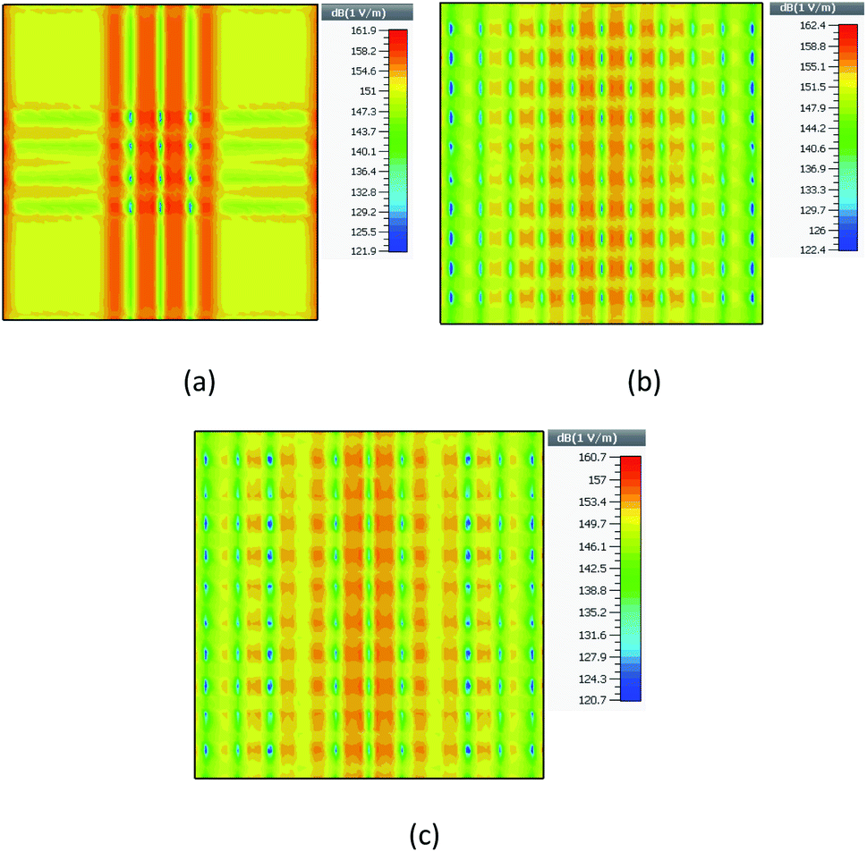 | ||
| Fig. 3 The electric field distribution for (a) Type-A at 290 THz, (b) Type-B at 240 THz, (c) Type-C at 230 THz. | ||
One of the main factors of the sensor elements is the uniformity of the field along the surface, which makes the sensing position independent. Due to the larger number of gold spheres in Types B and C, their gaps capacitance is larger than that of Type-A. So, they will have the higher E-field. However, the larger number of organic rods in Type-C leads to a wider distribution of the field. As a result, the electric field reduces in this case to 160.7 dB, as compared with Type-B with the electric field of 162.4 dB.
Regarding the results, the structure Type-B has better field distribution than the two other types. To adjust Type-B, the density and the conductivity of the DNA rods are increased, and the results are presented in Fig. 4. We assume the values of 100![[thin space (1/6-em)]](https://www.rsc.org/images/entities/char_2009.gif) 000 S m−1 and 1000 S m−1 for the high and low conductivity modes, respectively.
000 S m−1 and 1000 S m−1 for the high and low conductivity modes, respectively.
 | ||
| Fig. 4 Magnitude of the reflection comparison for the four states of conductivity and density of the DNA core–shell of Type-B. | ||
As shown in Fig. 4, the reflection in the low conductivity and low density mode is the same as the reflection in the low conductivity and high density mode. High conductivity and low density mode have lower reflection than low conductivity and low density mode. However, for high conductivity and high density mode, increasing the density leads to a decrease in both reflection and resonance frequency.
In fact, the conductivity of organic materials plays the role of resistance and inductance. They can be controlled by the values of density and conductivity. When the low conductivity is assumed for the organic material, the inductance and resistance value can be neglected. As shown in Fig. 4, the density does not have a considerable effect on the reflection in this mode. When the conductivity is increased, the value of this inductance and resistance cannot be ignored. It means that the inductance and resistance values are more than that in the low conductivity mode, and the higher inductance can reduce the operating frequency, while the resistance provides better matching and lower reflection.
Nanosphere with the DNA junction
Here, we analyze the characteristics of the Type-D structure, where DNA is located as a connection between the nanospheres. These connections give us two options. First, avoid the scattered fields. Second, field control is carried out by DNAs with different conductivity; thereby, absorption and electrical field improvement in these structures can be achieved. Various models can be suggested for this type of nanoparticles and junction between the central and peripheral nanospheres. Plus, the rods with higher conductivity can connect the nanospheres together and lessen their gap capacitance.Here, we propose three structures for Type-D, as shown in Fig. 5. The distance from the center of the nanosphere to the center of the other nanospheres has two values of 80 and 100 nm, and the results are compared for these two values.
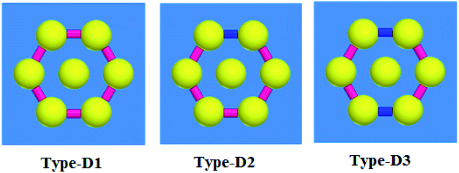 | ||
| Fig. 5 Proposed structures for Type-D1, D2 and D3. | ||
As already mentioned, the conductivity of the DNA can be controlled by combining the DNA with the nanoparticles of Ag, Au or Li. Thus, various conductivities can be assumed for the DNA-based rods. Two main types of conductivities are supposed for this absorber. In the first model, the low conductivity is defined as 1000 S m−1 (pink color).38 When the ratio of the metal NPs is increased in the DNA rod, the conductivity increases. The conductivity of 100000 S m−1 is for the high conductivity case (blue color). In Type-D1, all DNAs are assumed with low conductivity. For Type-D2, one junction is changed to high conductivity. In Type-D3, two junctions are changed to higher conductivity. These cases are selected among many possible cases for changing the two rods' conductivity to a higher value between six rods in Type-D3.
When nanospheres are placed near each other, the energy concentrates on their sides. It means that more energy is stored inside the unit cell, and the Q-factor of the structure increases as described by:
 | (2) |
Fig. 6(a) presents the reflection of the proposed structures for two distances between centers of the nanospheres, d = 80 and 100 nm. As seen here, Type-D3 has the best reflection at the distance of 80 nm, reaching −54 dB. Remarkably, the distance between the nanospheres is a contributory factor in the absorption. Structures with d = 80 nm distance between the centers of nanospheres have more absorption than d = 100 nm. Moreover, the other point is that decreasing the space in the structure will decrease the resonance frequency to a higher value. The reason for this decrease is the increase in the capacitance between nanospheres. Therefore, an increase in power saved in capacitors leads to reflection reduction and causes a higher Q-factor for the distance of 80 nm. To simulate these structures, we use the two-ports model (Fig. 6(b)). As shown in Fig. 6(c), high transmission of about −3 dB is reached beside a high reflection, which makes this nanostructure suitable as an opto-plasmonic sensor for both optical imaging and spectroscopy.
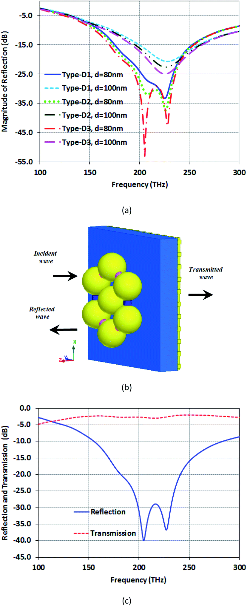 | ||
| Fig. 6 (a) Magnitude of reflection comparison of the proposed structures for two distances between the centers of the nanospheres of 80 and 100 nm. (b) Two-ports model. (c) Magnitude of transmission and reflection of structure Type-D3 at 80 nm distance. | ||
The field distribution of the proposed structures for the two distances, d = 80 and 100 nm, in their resonance frequency is presented in Fig. 7. As shown in Fig. 7(a), (c) and (e), for a distance of 80 nm, the fields of these structures are 164.9 (Type-D1), 166.1 (Type-D2), and 166.5 dB (Type-D3). However, for the structure with a distance of 100 nm as presented in Fig. 7(b), (d) and (f), it is reduced to 161.7 (Type-D1), 161.5 (Type-D2) and 162.6 dB (Type-D3), respectively. As can be seen, the Type-D3 structure has a higher maximum field than the other two in the same distance. It means that more electric field is stored in this nanostructure, and the Q-factor increases. On the other hand, the space between the nanospheres impacts the electric field. With a higher space, the electric field is reduced. Moreover, the electric field is distributed in a broader area for structures with d = 100 nm.
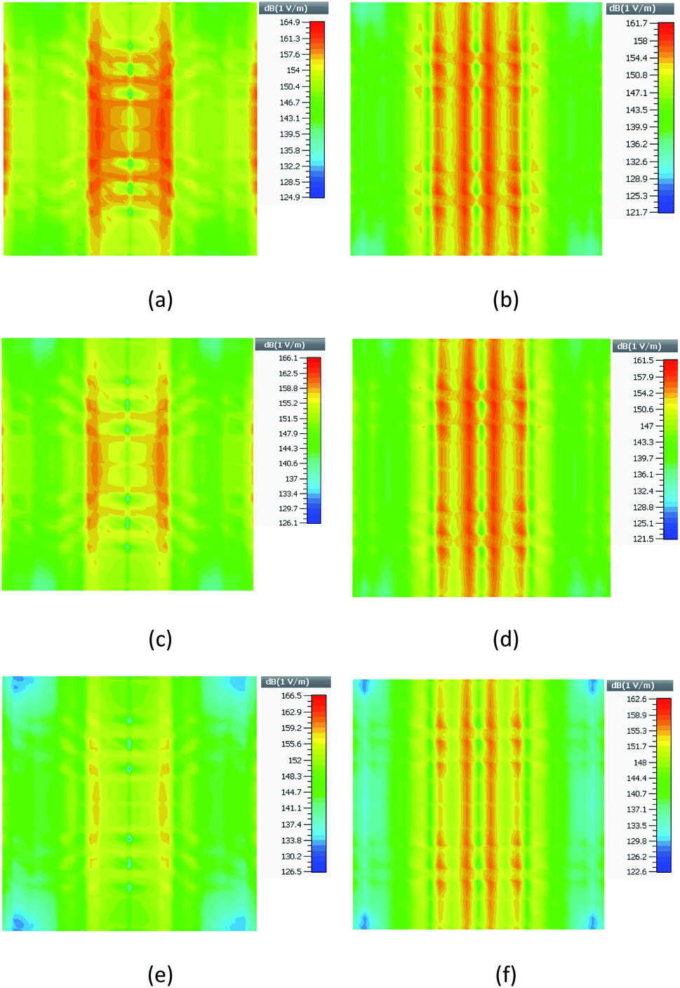 | ||
| Fig. 7 The electric field distribution for (a) Type-D1 with d = 80 nm, (b) Type-D1 with d = 100 nm, (c) Type-D2 with d = 80 nm, (d) Type-D2 with d = 100 nm, (e) Type-D3 with d = 80 nm, and (f) Type-D3 with d = 100 nm. | ||
Proposed structures as biosensors
We evaluate the proposed structures, Type-B, Type-C and Type-D3, as sensors based on some criteria. We consider a coating layer with 100 nm height containing the material under test (MUT), which covers the top of all the structures. The schematic of the Type-D3 sensor is shown in Fig. 8. The figure of merit (FOM) and sensitivity are used to quantify the performance of a sensor. Here, the FOM is defined by:51,52| FOM = ΔI(λ)/(I(λ) × Δn) | (3) |
 | (4) |
 | ||
| Fig. 8 The schematic of MUT over the structure as a biosensor. | ||
The S and FOM are obtained for Δn variations from 1 to 1.2 with steps of 0.05.
Fig. 9 presents variations of the magnitude of the reflection due to the small refractive index (RI) change for Type-B, Type-C and Type-D3. In the equivalent circuit of this structure, we can consider the capacitance increases with the permittivity and assume that the equivalent inductance is constant. We conclude from  that the higher capacitance leads to lower resonance frequency.
 | ||
| Fig. 9 Reflection magnitude and resonance frequency for different values of refractive indices MUT for (a) Type-A, (b) Type-B, (c) Type-C, (d) Type-D1, (e) Type-D2, and (f) Type-D3. | ||
Fig. 9(a)–(f) show the magnitude of reflection and resonance frequency for different values of refractive indices of MUT for Type-A, Type-B, Type-C, Type-D1, Type-D2 and Type-D3. The magnitudes of the reflections for Type-B and Type-D3 are near zero at the resonance frequencies (198 THz for Type-B, 202 and 227 THz for Type-D3). Thus, they have higher FOM as compared with Type-C.
Fig. 10(a) shows the plots of magnitude of reflection of these types of sensors at their resonance frequencies versus variation of RI. Based on the RI effect on the variation of the magnitude of reflection (ΔI), the FOM of these types of sensors is calculated. The values of I for Type-B and Type-C are 0.0043 and 0.19, respectively, at their resonance frequencies. For Type-D3, the values are 0.005 and 0.0025 at its two resonance frequencies. Fig. 10(b) shows the plots of resonance wavelength shift versus variation of RI for these types of sensors. This study shows that the sensitivity for the first resonance (f1) is better than that of the second resonances (f2) in Type-D1, Type-D2 and Type-D3, and the FOM for the second resonances in Type-D1 and Type-D2 is more than that of the first resonance. So, by selecting a special arrangement of DNA rods with different conductivities, we can modify the sensitivity and FOM for the proposed absorber.
 | ||
| Fig. 10 The plots of (a) reflection magnitude versus variation of RI at sensor resonance frequencies, and (b) resonance wavelength shift versus variation of RI for the proposed types of sensor. | ||
The FOM and S of these types of optical sensors are checked in Table 1. While it shows that Type-C has a low FOM, which is about 3 RIU−1, it has a high S of about 1287 nm RIU−1.
| Structure type | Frequency (THz) | FOM (RIU−1) | Sensitivity (nm RIU−1) |
|---|---|---|---|
| Type-A | f = 291.2 | 5 | 737 |
| Type-B | f = 198.4 | 130 | 1079 |
| Type-C | f = 228 | 3 | 1287 |
| Type-D1 | f1 = 202 | 92 | 1289 |
| Type-D1 | f2 = 227.2 | 26 | 781 |
| Type-D2 | f1 = 208 | 80 | 1206 |
| Type-D2 | f2 = 223.6 | 189 | 72 |
| Type-D3 | f1 = 202 | 218 | 1000 |
| Type-D3 | f2 = 227.2 | 340 | 521 |
The FOM of Type-D3 at f1 and f2 is 218 RIU−1 and 340 RIU−1, respectively. The dual-resonance characteristics of the structure can be used for enhancing the quality of sensing by comparing unknown materials. Type-D3 has the best FOM between these structures. Type-B shows the medium FOM and sensitivity of 130 RIU−1 and S 1079 (nm RIU−1).
These sensors can be used for both gas and aqueous biological samples. Recently, various models of nanoabsorbers, nanoapertures, and metasurfaces have been developed as optical sensors. Type-D3 (at f1) is compared with some sensors from previous research studies in Table 2. As we observe, our sensor has high values for both FOM and sensitivity, as compared with the other sensors. The other advantage is its dual-resonance characteristics.
Cancer cell detection
In this section, to detect infected skin tissues from healthy ones, we examine the structure Type-B at high density and high conductivity mode.The use of living cells in the diagnosis of cancer is very much considered. Many scientific efforts have been made to reveal the biological properties of cancer cells for monitoring and detecting the pathway of cancer spread.56 It is well-known in cancer biology that the index of cancer cells is higher than healthy cells. The imaginary part of the refractive index for skin cells is less than 64 × 10−4 in the optical spectrum. These values have been extracted by light extinction estimates technique based on absorption and scattering;57 so, we can neglect it. The refractive indices of skin cells and cancerous ones are about 1.35 and 1.45, respectively.56–59 In this study, the healthy and cancer cells are modeled based on previous practical studies.
Here, a tissue with a thickness of 20 nm is put below the fishnet layer. We assume the refractive index of 1.45 and 1.35 for the cancerous and the healthy skin tissue, respectively. We propose two distribution models, concentrated and non-concentrated for cancerous skin tissue, as shown in Fig. 11(a) and (b), respectively. We perform simulations for different percentages of tissue infections for both distribution models of cancer cells in the skin tissue. Here, we focus on designing a sensor independent of a distribution model of cancerous cells. As mentioned in ref. 59 and 60, so far, there is no exact value for the permittivity of the cancer or healthy cells. Thus, in this study, we assume a periodic boundary condition with some distribution models to predict how much of an impact the distribution models can have on the reflection of the sensor. On the other hand, the arbitrary shape of the nanosurface can alter the phase of the optical wave, which has the same effect as the material variation,61 and this phase variation can be modeled by the distribution model.
 | ||
| Fig. 11 The schematic of two distribution models (a) concentrated and (b) non-concentrated for cancerous skin tissue. | ||
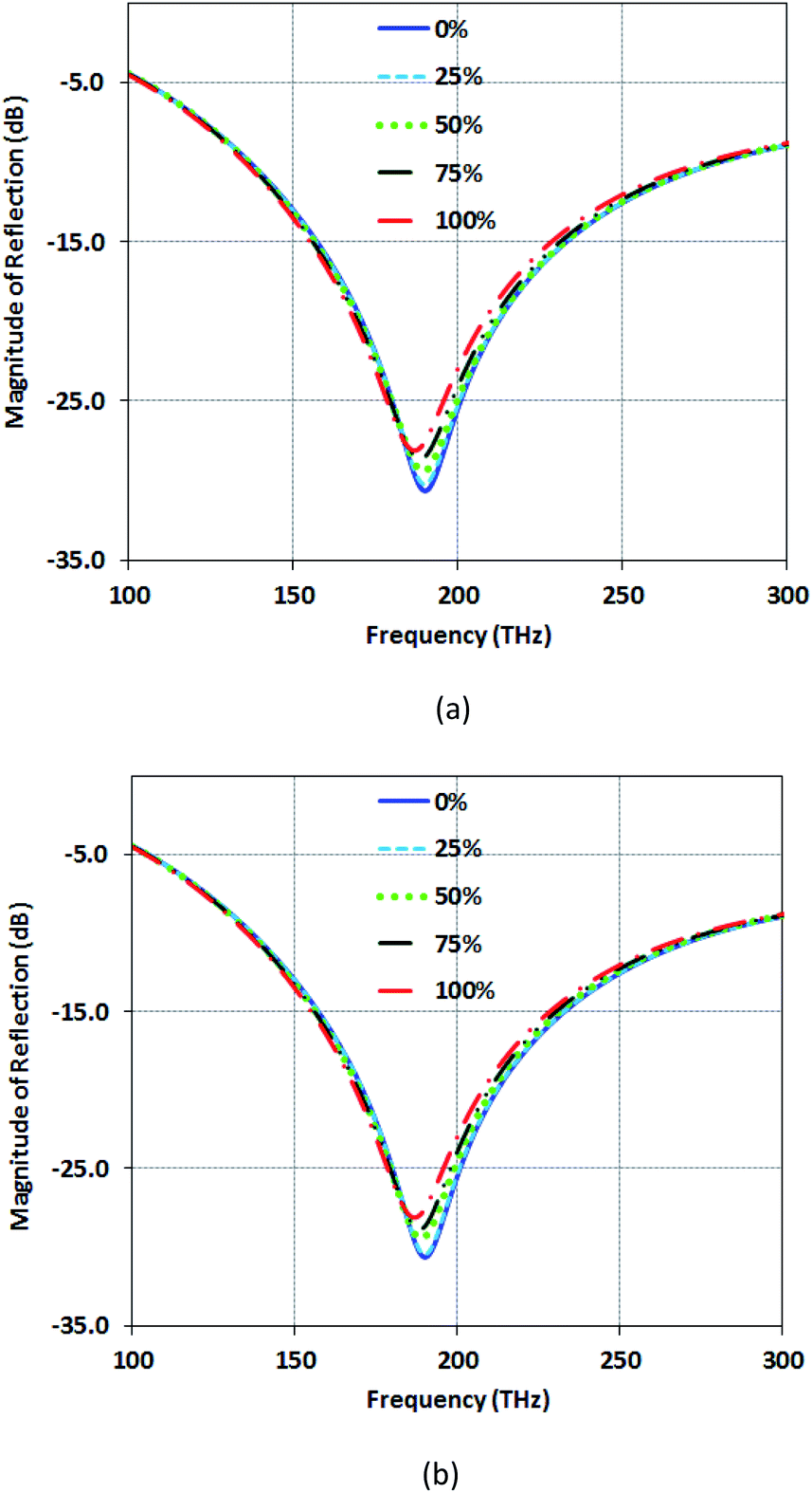
In Fig. 12(a), the reflection magnitude for the concentrated distribution model rises from −31 dB for healthy skin tissue to −28 dB for cancerous tissue at its resonance frequency. Also, in Fig. 12(b), the reflection magnitude for the non-concentrated distribution model (similar to Fig. 12(a)), rises from −31 dB for healthy skin tissue to −28 dB for cancerous tissue. This increase of reflection originates from a larger RI of cancerous tissue than the healthy tissue. For higher percentages of the cancerous tissue, the effective refractive index (neff) of the tissue gets larger, and the capacitance of the tissue under test also increases. The larger capacitance causes the shift to a lower frequency, as shown in Fig. 12(a) and (b). The structure Type-B shows the reflection with the narrow band response. So, it is interesting for optical sensing.
 | ||
| Fig. 12 Magnitude of reflection (dB) for various percentages of cancerous cells for Type-B structure (a) with the concentrated model (b) with a non-concentrated model for cancer cells. | ||
Many types of organic materials, such as red and white blood cells and healthy and cancerous skin cells, have refractive indices in the range of 1.35 to 1.45.58 So, the structure Type-B can be used as a sensor for these materials. Fig. 13 shows that the magnitude of reflection for refractive indices varies from 1.35 to 1.45 under Type-B structure. We can see, as the RI increases, the magnitude of reflection rises to higher values and the resonance frequency is red-shifted. Comparing the results of Fig. 12 and 13 shows that Type-B as a sensor can distinguish materials independent of arrangement and the locations of cells in the samples. This characteristic originates from the high Q-factor resonance of Type-B and the reflection only depends on neff.
 | ||
| Fig. 13 Magnitude of reflection for various RI of materials under the Type-B structure. | ||
Conclusions
In this paper, plasmonic arrays composed of GNPs are studied. Several engineered structures based on the opto-plasmonic effect were proposed. We have used DNA-GNP core–shells and DNA rods as junctions between GNPs for controlling and improving the absorbance. In order to transfer and reflect electromagnetic waves from the biological surface, we have designed the underlying gold layer as a fishnet. The heptamer structure with DNA-GNP core–shells has a uniform electric field, which makes it suitable for distinguishing the cancerous tissue, regardless of the arrangement and location of the cancer cells. On the other hand, these DNA-GNPs structures were used as sensors. The results showed that we could obtain a sensitivity of more than 1000 nm RIU−1. The structure based on the DNA rods as junctions between GNPs shows the best FOM value of 340 RIU−1. The dual-resonance characteristics of this structure can be used for enhancing the quality of sensing by comparing unknown materials. The core–shell heptamer structure has the best sensitivity of about 1287 nm RIU−1. The comparison with previous research showed that these sensors, because of their high sensitivity and dual-resonance characteristics, could be used for both material detection and optical imaging.Conflicts of interest
There are no conflicts to declare.Notes and references
- M. Giloan and S. Astilean, Negative index optical chiral metamaterial based on asymmetric hexagonal arrays of metallic triangular nanoprisms, Opt. Commun., 2014, 315, 122–129 CrossRef CAS.
- X. Jing, W. Wang, R. Xia, J. Zhao, Y. Tian and Z. Hong, Manipulation of dual band ultrahigh index metamaterials in the terahertz region, Appl. Opt., 2016, 55(31), 8743–8751 CrossRef PubMed.
- J. Zhang and N. Asger Mortensen, Ultrathin cylindrical cloak, Prog. Electromagn. Res., 2011, 121, 381–390 CrossRef.
- H.-W. Yoo, L. J. Richter, H.-T. Jung and C. A. Michaels, Surface plasmon polariton Raman microscopy, Vib. Spectrosc., 2012, 60, 85–91 CrossRef CAS.
- M. Zhong and Y. Ye, Role of coupling of localized surface plasmon modes in transmission properties of compound structure metamaterials, Opt. Commun., 2015, 335, 94–98 CrossRef CAS.
- Z. L. Mei and T. J. Cui, Experimental realization of a broadband bend structure using gradient index metamaterials, Opt. Express, 2009, 17(20), 18354–18363 CrossRef CAS.
- R. Ning, J. Bao, Z. Chen and Z. Jiao, Electromagnetically induced absorption in metamaterials and applications in the infrared range, J. Electron. Mater., 2019, 48(7), 4733–4739 CrossRef CAS.
- G. Deng, J. Yang and Z. Yin, Broadband terahertz metamaterial absorber based on tantalum nitride, Appl. Opt., 2017, 56(9), 2449–2454 CrossRef CAS PubMed.
- S. Khosravi, A. Rostami, G. Rostami and M. Dolatyari, Midinfrared invisibility cloak design using composite optical materials, IEEE J. Sel. Top. Quantum Electron., 2016, 22(1), 134–139 Search PubMed.
- N. M. Estakhri and A. Alu, Minimum-scattering superabsorbers, Phys. Rev. B: Condens. Matter Mater. Phys., 2014, 89(12), 121416 CrossRef.
- Y. Cheng, F. Yang, J. Yi Xu and X. J. Liu, A multilayer structured acoustic cloak with homogeneous isotropic materials, Appl. Phys. Lett., 2008, 92(15), 151913 CrossRef.
- D. Diedrich, A. Rottler, D. Heitmann and S. Mendach, Metal–dielectric metamaterials for transformation-optics and gradient-index devices in the visible regime, New J. Phys., 2012, 14(5), 053042 CrossRef.
- M. G. Silveirinha, A. Alù and N. Engheta., Cloaking mechanism with antiphase plasmonic satellites, Phys. Rev. B: Condens. Matter Mater. Phys., 2008, 78(20), 205109 CrossRef.
- M. T. T. Nguyen, D. H. Nguyen, My T. Pham, H. V. Pham and C. D. Huynh, Synthesis and Vertical Self-Assembly of Gold Nanorods for Surface Enhanced Raman Scattering, J. Electron. Mater., 2019, 48(8), 4970–4976 CrossRef CAS.
- Y. Ren, S. Hu, B. Ji, P. Zou, L. Liu and Y. Li, Fano resonance in Al nano-dolmen plasmonic structure for enhanced biosensing, Sensing and Bio-Sensing Research, 2017, 15, 5–11 CrossRef.
- A. Ahmadivand, S. Golmohammadi, M. Karabiyik and N. Pala, Fano resonances in complex plasmonic necklaces composed of gold nanodisks clusters for enhanced LSPR sensing, IEEE Sens. J., 2014, 15(3), 1588–1594 Search PubMed.
- E. Aslan, E. Aslan, M. Turkmen and O. G. Saracoglu, Metamaterial plasmonic absorber for reducing the spectral shift between near-and far-field responses in surface-enhanced spectroscopy applications, Sens. Actuators, A, 2017, 267, 60–69 CrossRef CAS.
- R. Adato, A. A. Yanik and H. Altug, On chip plasmonic monopole nano-antennas and circuits, Nano Lett., 2011, 11(12), 5219–5226 CrossRef CAS.
- P. Biagioni, M. Savoini, J.-S. Huang, L. Duò, M. Finazzi and B. Hecht, Near-field polarization shaping by a near-resonant plasmonic cross antenna, Phys. Rev. B: Condens. Matter Mater. Phys., 2009, 80(15), 153409 CrossRef.
- J. Chen, K. He and Z. Zhang, Triangle defects in bowtie nanoantennas, Appl. Phys. A: Mater. Sci. Process., 2013, 112(3), 591–596 CrossRef CAS.
- A. E. Cetin and H. Altug, Fano resonant ring/disk plasmonic nanocavities on conducting substrates for advanced biosensing, ACS Nano, 2012, 6(11), 9989–9995 CrossRef CAS PubMed.
- S.-D. Liu, Z. Yang, R.-P. Liu and X.-Y. Li, Multiple Fano resonances in plasmonic heptamer clusters composed of split nanorings, ACS Nano, 2012, 6(7), 6260–6271 CrossRef CAS.
- E. Aslan, E. Aslan, M. Turkmen and O. G. Saracoglu, Experimental and numerical characterization of a mid-infrared plasmonic perfect absorber for dual-band enhanced vibrational spectroscopy, Opt. Mater., 2017, 73, 213–222 CrossRef CAS.
- Y. Wang, T. Sun, T. Paudel, Y. Zhang, Z. Ren and K. Kempa, Metamaterial-plasmonic absorber structure for high efficiency amorphous silicon solar cells, Nano Lett., 2011, 12(1), 440–445 CrossRef.
- R. Adato and H. Altug, In-situ ultra-sensitive infrared absorption spectroscopy of biomolecule interactions in real time with plasmonic nanoantennas, Nat. Commun., 2013, 4, 2154 CrossRef.
- H. Durmaz, Y. Li and A. E. Cetin, A multiple-band perfect absorber for SEIRA applications, Sens. Actuators, B, 2018, 275, 174–179 CrossRef CAS.
- C. Ding, L. Jiang, L. Wu, R. Gao, D. Xu, G. Zhang and J. Yao, Dual-band ultrasensitive THz sensing utilizing high quality Fano and quadrupole resonances in metamaterials, Opt. Commun., 2015, 350, 103–107 CrossRef CAS.
- A. Tittl, A. John-Herpin, A. Leitis and R. Eduardo, Arvelo, and Hatice Altug. "Metasurface-based molecular biosensing aided by artificial intelligence, Angew. Chem., Int. Ed., 2019, 58(42), 14810–14822 CrossRef CAS.
- R. Cheng, L. Xu, X. Yu, L. Zou, Y. Shen and X. Deng, High-sensitivity biosensor for identification of protein based on terahertz Fano resonance metasurfaces, Opt. Commun., 2020, 125850 CrossRef CAS.
- H. Zhang, Z. Li, F. Hu, T. Chen, B. Qin and Y. Zhao, Sensitive detection of chlorpheniramine maleate using THz combined with metamaterials, Opt. Quantum Electron., 2017, 49(8), 258 CrossRef.
- E. Aslan and M. Turkmen, Square fractal-like nanoapertures for SEIRA spectroscopy: An analytical, numerical and experimental study, Sens. Actuators, A, 2017, 259, 127–136 CrossRef CAS.
- W. Yang, J. Lu, E. P. Gilbert, R. Knott, L. He and W. Cheng, Probing soft corona structures of DNA-capped nanoparticles by small angle neutron scattering, J. Phys. Chem. C, 2015, 119(32), 18773–18778 CrossRef CAS.
- S. J. Tan, M. J. Campolongo, D. Luo and W. Cheng, Building plasmonic nanostructures with DNA, Nat. Nanotechnol., 2011, 6(5), 268 CrossRef CAS PubMed.
- D.-K. Lim, K.-S. Jeon, J.-H. Hwang, H. Kim, S. Kwon, Y. D. Suh and J.-M. Nam, Highly uniform and reproducible surface-enhanced Raman scattering from DNA-tailorable nanoparticles with 1-nm interior gap, Nat. Nanotechnol., 2011, 6(7), 452 CrossRef CAS.
- S. A. Maier, Plasmonics: fundamentals and applications, Springer Science & Business Media, 2007 Search PubMed.
- P. B. Johnson and R.-W. Christy, Optical constants of the noble metals, Phys. Rev. B: Solid State, 1972, 6(12), 4370 CrossRef CAS.
- Y. Wang, X. Yan and R. Dong, Organic memristive devices based on silver nanoparticles and DNA, Org. Electron., 2014, 15(12), 3476–3481 CrossRef CAS.
- S. Qin, R. Dong, X. Yan and Q. Du, A reproducible write–(read) n–erase and multilevel bio-memristor based on DNA molecule, Org. Electron., 2015, 22, 147–153 CrossRef CAS.
- S. M. D. Watson, A. R. Pike, J. Pate, A. Houlton and B. R. Horrocks, DNA-templated nanowires: morphology and electrical conductivity, Nanoscale, 2014, 6(8), 4027–4037 RSC.
- V. Hodzic, V. Hodzic and R. W. Newcomb, Modeling of the electrical conductivity of DNA, IEEE Trans. Circuits Syst. I: Regul. Pap., 2007, 54(11), 2360–2364 Search PubMed.
- Z. Kutnjak, G. Lahajnar, C. Filipič, R. Podgornik, L. Nordenskiöld, N. Korolev and A. Rupprecht, Electrical conduction in macroscopically oriented deoxyribonucleic and hyaluronic acid samples, Phys. Rev. E: Stat., Nonlinear, Soft Matter Phys., 2005, 71(4), 041901 CrossRef.
- F. El-Diasty and F. Abdel-Wahab, Optoelectronic studies on heterocyclic bases of deoxyribonucleic acid for DNA photonics, Mater. Sci. Eng. C, 2015, 55, 524–529 CrossRef CAS.
- S. Bhattacharya, J. Choi, S. Lodha, D. B. Janes, A. F. Bonilla, K. J. Jeong, and G. U. Lee, Electronic conduction in DNA attached to gold electrodes, in 2003 Third IEEE Conference on Nanotechnology, 2003. IEEE-NANO 2003, IEEE, 2003, vol. 1, pp. 79–82 Search PubMed.
- J. Richter, M. Mertig, W. Pompe, I. Mönch and H. K. Schackert, Construction of highly conductive nanowires on a DNA template, Appl. Phys. Lett., 2001, 78(4), 536–538 CrossRef CAS.
- Y. Z. Cheng, Y. Nie and R. Z. Gong, Broadband 3D isotropic negative-index metamaterial based on fishnet structure, Eur. Phys. J. B, 2012, 85(2), 62 CrossRef.
- D. Rodrigo, Andreas Tittl, Aurelian John-Herpin, Odeta Limaj, and Hatice Altug. "Self-Similar Multiresonant Nanoantenna Arrays for Sensing from Near-to Mid-Infrared, ACS Photonics, 2018, 5(12), 4903–4911 CrossRef CAS.
- H. D. Hill, J. E. Millstone, M. J. Banholzer and C. A. Mirkin, The role radius of curvature plays in thiolated oligonucleotide loading on gold nanoparticles, ACS Nano, 2009, 3(2), 418–424 CrossRef CAS PubMed.
- S. J. Tan, J. S. Kahn, T. L. Derrien, M. J. Campolongo, M. Zhao, D. -M. Smilgies and D. Luo, Crystallization of DNA-Capped Gold Nanoparticles in High-Concentration, Divalent Salt Environments, Angew. Chem., Int. Ed., 2014, 53(5), 1316–1319 CrossRef CAS PubMed.
- Q. Zhang, J. You and C. Liu, Equivalent Nanocircuit Theory and Its Applications, Nanoplasmonics: Fundam. Appl., 2017, 362–356 CAS.
- M. Danaie and B. Kiani, Design of a label-free photonic crystal refractive index sensor for biomedical applications, Photonics Nanostructures: Fundam. Appl, 2018, 31, 89–98 CrossRef.
- G. Zheng, X. Zou, Y. Chen, L. Xu and W. Rao, Fano resonance in graphene-MoS2 heterostructure-based surface plasmon resonance biosensor and its potential applications, Opt. Mater., 2017, 66, 171–178 CrossRef CAS.
- N. Liu, M. Mesch, T. Weiss, M. Hentschel and H. Giessen, Infrared perfect absorber and its application as plasmonic sensor, Nano Lett., 2010, 10(7), 2342–2348 CrossRef CAS PubMed.
- R. Zafar and M. Salim, Enhanced figure of merit in Fano resonance-based plasmonic refractive index sensor, IEEE Sens. J., 2015, 15(11), 6313–6317 CAS.
- R. Ameling, L. Langguth, M. Hentschel, M. Mesch, P. V. Braun and H. Giessen, Cavity-enhanced localized plasmon resonance sensing, Appl. Phys. Lett., 2010, 97(25), 253116 CrossRef.
- A. D. Khan, Refractive index sensing with fano resonant L-shaped metasurface, Opt. Mater., 2018, 82, 168–174 CrossRef CAS.
- G.-D. Liu, Z. Xiang, L.-L. Wang, Qi Lin, S.-X. Xia, X. Luo and C.-J. Zhao, A high-performance refractive index sensor based on Fano resonance in Si split-ring metasurface, Plasmonics, 2018, 13(1), 15–19 CrossRef CAS.
- P. Giannios, K. G. Toutouzas, M. Matiatou, K. Stasinos, M. M. Konstadoulakis, G. C. Zografos and K. Moutzouris, Visible to near-infrared refractive properties of freshly-excised human-liver tissues: marking hepatic malignancies, Sci. Rep., 2016, 6, 27910 CrossRef CAS PubMed.
- E. V. Salomatina, B. Jiang, J. Novak and A. N. Yaroslavsky, Optical properties of normal and cancerous human skin in the visible and near-infrared spectral range, J. Biomed. Opt., 2006, 11(6), 064026 CrossRef PubMed.
- W. J. Choi, D. I. Jeon, S.-G. Ahn, J.-H. Yoon, S. Kim and B. H. Lee, "Full-field optical coherence microscopy for identifying live cancer cells by quantitative measurement of refractive index distribution, Opt. Express, 2010, 18(22), 23285–23295 CrossRef CAS PubMed.
- Q. Zhang, L. Zhong, P. Tang, Y. Yuan, S. Liu, J. Tian and X. Lu, Quantitative refractive index distribution of single cell by combining phase-shifting interferometry and AFM imaging, Sci. Rep., 2017, 7(1), 1–10 CrossRef.
- X. Ni, Z. J. Wong, M. Mrejen, Y. Wang and X. Zhang, An ultrathin invisibility skin cloak for visible light, Science, 2015, 349(6254), 1310–1314 CrossRef CAS.
| This journal is © The Royal Society of Chemistry 2021 |