DOI:
10.1039/D1RA02702F
(Paper)
RSC Adv., 2021,
11, 17445-17455
Band engineering of Dirac materials in SbmBin lateral heterostructures†
Received
7th April 2021
, Accepted 30th April 2021
First published on 13th May 2021
Abstract
Band engineering the electronic structures of SbmBin lateral heterostructures (LHS) from antimonene and bismuthene is systematically investigated using first principles calculations. The spin–orbit coupling is found to be crucial in determining electronic structures of SbmBin LHS. The results indicate that these lateral heterostructures have a type-II band alignment which can be easily tuned using their size and tensile strain. The band gap tends to zero when the lateral heterostructure size is larger than a critical value, which intrinsically corresponds to a semiconductor-to-semimetal transition. The band inversion near the Γ point occurs under suitable tensile strain, indicating that SbmBin LHS are very promising to realize quantum spin Hall effects.
1. Introduction
Heterojunctions between three-dimensional (3D) semiconductors with different band gaps form the basis of modern light-emitting diodes1 and high-speed transistors.2 Similar to the conventional 3D heterojunctions, two-dimensional (2D) heterojunctions comprise two kinds of nanomaterials with different electron affinities and band gaps.3–5 Consequently, they exhibit excellent optoelectronic performance, which cannot be achieved by the individual nanomaterials. Therefore, 2D heterojunctions provide many new opportunities for tailoring the electronic and transport properties as well as for realizing novel device architectures. To utilize 2D crystalline semiconductors as building blocks for next-generation electronics, the exploration of new 2D heterojunctions is crucial. In general, two types of 2D heterostructures can be synthesized: vertical heterostructures (VHS) and lateral heterostructures (LHS). VHS can be obtained by vertical stacking of 2D crystals in a layered configuration on top of each other,6–8 and their properties are dominated by the stacking orientation and interlayer coupling strength. However, the poor controllability of band structures in VHS limits its practical applications. In contrast, LHS represent a new class of designer materials that can be composed of a variety of 2D materials, which are structurally and mechanically similar but exhibit entirely different electronic and optical properties. Spatially connected LHS exhibit two surfaces and simpler band alignment as compared to VHS, and their electrical and optical properties are intrinsically dominated by the band alignment at the heterointerfaces. Further, the domains in LHS are usually connected by covalent bonds, which ensure the epitaxial quality of the interface, thereby boosting the optical and electrical properties of the heterostructures.9,10 These attributes of LHS have motivated significant efforts in the exploration of new heterostructures with unique properties.
The recent advances in the synthesis and characterization of monoatomic thick materials have facilitated the fabrication of various 2D LHS including graphene/h-BN11 and transition metal dichalcogenides (TMD).12–14 However, it is always a great challenge to synthesize 2D LHS with clean heterointerfaces, which are very important in the field of high performance devices.15–17 VHS have been fabricated using chemical vapor deposition (CVD)18 and other advanced synthetic methods. Fortunately, CVD is also used for epitaxial growth of LHS,19 which can offer precise spatial control to achieve atomically sharp transition in compositions at the heterojunction. Consequently, several LHS have been synthesized by this technique. For example, Zhang et al.10 proposed a synthetic method for highly robust epitaxial growth of diverse LHS and superlattices with atomically sharp interfaces. Hong et al.20 demonstrated the synthesis and practical applications of graphene/MoS2 LHS, indicating that the choice of a suitable MoS2 growth temperature is crucial for the synthesis process. Further, an atomically sharp zigzag-like boundary has been observed to dominate the patching interface of graphene/h-BN,21 MoS2/WS2 (ref. 22) and MoSe2/WSe2.23 Nevertheless, so far, suitable basis materials available for synthesizing LHS are extremely limited. Therefore, it is crucial to explore such materials to synthesize novel LHS.
Recently, nanomaterials formed by group VA elements such as phosphorene, arsenene, antimonene, and bismuthene have emerged as a novel type of 2D materials, which exhibit intriguing structures and properties, leading to a wide range of applications in electronics and optoelectronics.24–27 Phosphorene is the first material in this family; recently, it was mechanically isolated from bulk phosphorus and has already been used to fabricate transistors.28,29 Unfortunately, phosphorene is very unstable and is rapidly oxidized by the atomic layer deposition process.30,31 In addition, during the synthesis process of arsenene, highly toxic arsenic trioxide can be produced, which hinders the experimental exploration of arsenene.32 Unlike unstable phosphorene, antimonene and bismuthene are predicted to exhibit good stability and remarkable physical properties.33,34 Antimonene is an indirect-band gap semiconductor with an optical gap of 2.28 eV,35 while its band gap with spin–orbit coupling (SOC) is 0.76 eV.36 By contrast, bismuthene is a direct-band gap semiconductor with an optical gap of 0.55 eV (ref. 37 and 38) and exhibits a cone-like structure near Γ point. However, when SOC is included, the degenerate bands at the top of the valence band at the Γ point exhibit a Rashba-type splitting and reduce the band gap to 0.51 eV (ref. 39) by changing its character from direct-to indirect-band gap. Notably, under appropriate tensile strain, antimonene not only transforms from indirect-to direct-band gap semiconductor but also exhibits band inversion, indicating that they are very promising to realize quantum spin Hall effect (QSHE).35,36 Besides, a novel quantum spin Hall state with tunable edge states has been predicted in a structure of antimonene and bismuthene on suitable substrates.40,41 The substrate induces a drastic staggered exchange field in 2D film, which plays a vital role in generating the QSHE. All these merits of 2D materials motivated us to design LHS based on them.
Herein, we systematically investigate the band engineering of SbmBin LHS (m and n denote the number of Sb or Bi atomic chains) at the zigzag interface via first-principles calculations. SOC is found to be crucial in determining the electronic structures. We observed that all the stable SbmBin LHS exhibit a type-II band alignment and relatively small band gaps (0.004–0.254 eV) as comparing with initial antimonene and bismuthene. For m = n, SbmBin LHS are confirmed to be Dirac materials, which exhibit a Dirac cone near the Fermi level. SbmBin LHS are very similar to spin-valley-coupled Dirac semimetals, whose massless Dirac fermions are fully spin polarized.26 For m ≠ n, SbmBin LHS are confirmed to be semiconductor materials. Therefore, we have demonstrated that SbmBin LHS can maintain the Dirac semimetallic character only if the condition m ≈ n is satisfied. Additionally, the size of SbmBin LHS is one of the crucial parameters that govern its electronic and optical performance. It is similar to the size dependent band gaps of TMD LHS;42 the band gap of SbmBin LHS tend to zero when the size is larger than the critical value, which essentially corresponds to the transition from semiconductor to semimetal. Besides, the orbital-projected band structure indicates that the Bi-py orbitals dominate the energy band near the Fermi level, while the orbitals of Sb atoms have a minor effect on it. It is reasonable to ignore the effect of the orbitals of Sb atoms on the energy bands of SbmBin LHS. The orbital-projected band structure demonstrates that the band inversion near Γ point occurs on suitable tensile strain, indicating that SbmBin LHS are very promising to realize QSHE. Therefore, we believe that the excellent properties of SbmBin LHS realized in this study will inspire further theoretical as well as experimental investigations on these materials.
2. Computational methods
Here, all the structural relaxation and electronic calculations are based on density functional theory (DFT) implemented in the Vienna ab initio simulation package (VASP).43,44 The exchange-correlation functional was treated within the generalized gradient approximation (GGA) and parameterized by Perdew–Burke–Ernzerhof (PBE)45 functional. Sb and Bi are heavy atoms, hence SOC must take into account in the calculation of electronic structures. The long-range van der Waals interaction between atomic layers was taken into account by employing the semi-empirical dispersion-corrected D3 scheme proposed by Grimme.46 A cutoff energy of the plane wave was set to 550 eV. The k-point sampling in the Brillouin zone was implemented by the Monkhorst–Pack scheme, where 16 × 16 × 1 and 2 × 9 × 1 grids were used for optimizing the geometry of pristine antimonene (or bismuthene) and SbmBin LHS, respectively. All atoms were optimized until the variations in the total energy and residual force were less than 10−5 eV and 10−2 eV Å−1, respectively. To avoid the interaction between adjacent layers, a vacuum spacing of 15 Å was added along the direction perpendicular to the 2D sheet. As GGA method underestimates the band gap of semiconductor materials, the Heyd–Scuseria–Ernzerhof screened hybrid functional (HSE06)47 was used to compute the electronic and optical properties of SbmBin LHS. The charge density difference and work function was calculated using VASPKIT code.48
3. Results and discussion
3.1 Structural properties
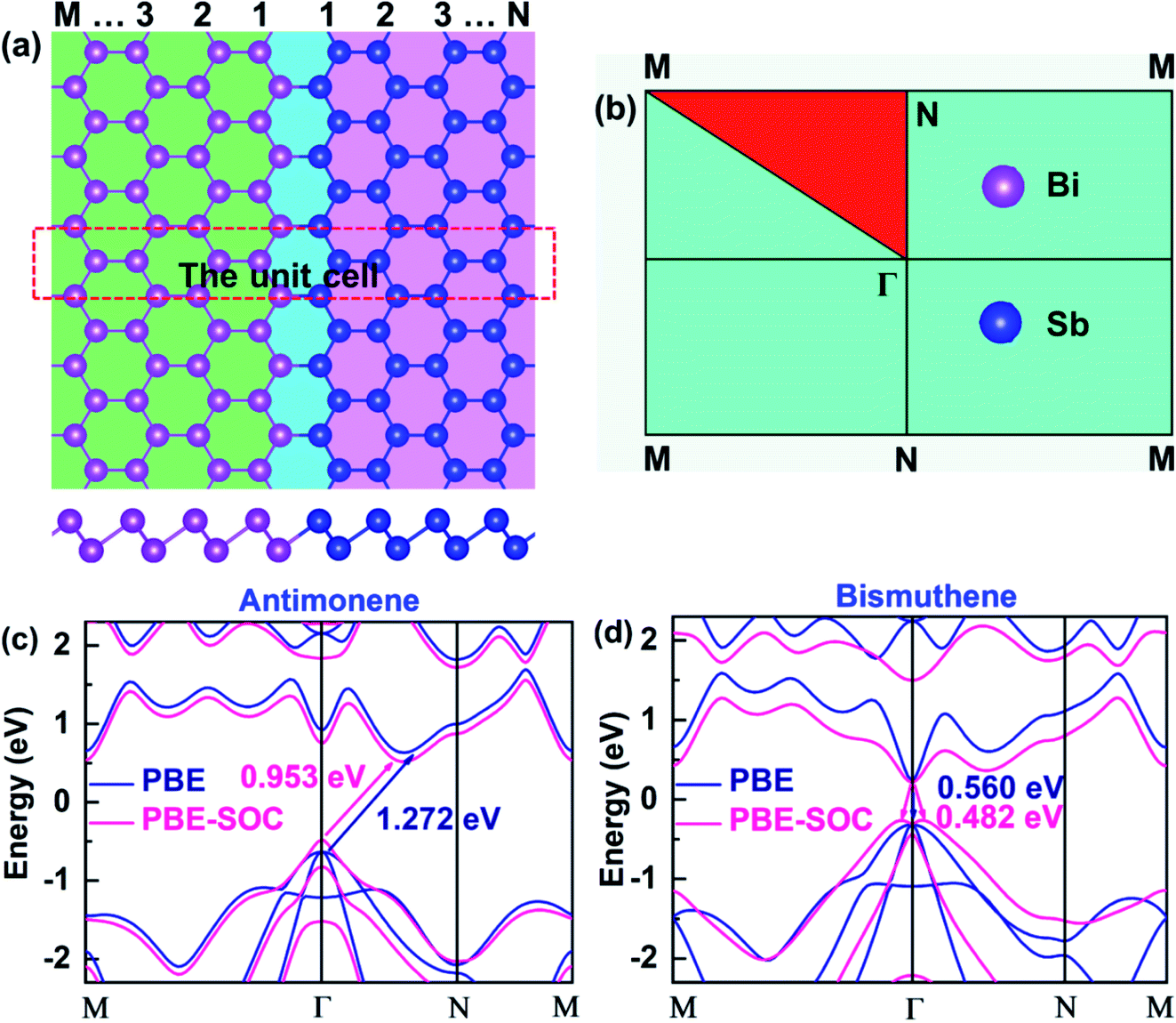
According to recent studies, high-quality 2D LHS such as graphene/h-BN11 and TMD12–14 with atomically sharp interfaces along armchair or zigzag direction have been fabricated via CVD method. In heterointerfaces, the zigzag boundaries are preferably formed, while the armchair interfaces, which usually have many defects, are rarely observed. Therefore, we simulate SbmBin LHS with zigzag-type interface using first-principles calculation. The fully optimized SbmBin LHS are shown in Fig. 1(a), where the indices m and n denote the number of Sb or Bi atomic chains. Here, we fix the lattice constant of the Z axis and fully relax the lattice constants in the X and Y directions, so all atoms of LHS are fully relaxed, and their energies and forces are optimized to reach the minimum values with 10−5 eV and 10−2 eV Å−1, respectively. The bond length and unit cells of LHS are illustrated in Table S1.† We found that the lattice constant a increases, but that of b remains a constant value about 4.24 Å with the increase of the width of the heterojunction. Sb–Sb and Bi–Bi bond length of the antimonene and bismuthene are 2.89 Å and 3.04 Å, respectively. However, the average bond lengths of Sb–Sb, Sb–Bi, and Bi–Bi in the LHS are 2.90, 2.97, and 3.04. Comparing bond lengths between the antimonene, bismuthene and LHS, it is found that the Sb–Sb bond length is elongated from 2.89 Å to 2.90 Å, while the Sb–Bi and Bi–Bi bond length remains almost a constant value. Besides, the antimonene and bismuthene (Fig. 1(c) and (d)), basic structural units of SbmBin LHS, are observed to be indirect band gap semiconductors under SOC with optical gaps of 0.953 and 0.482 eV, which is in good agreement with earlier studies.36,37 The calculation results reveal that the valence band maximum (VBM) of antimonene and bismuthene has a degenerate character of px and py orbitals. Particularly, VBM at the Γ point of bismuthene exhibits a Rashba-type splitting under SOC, which changes its character from direct band gap to indirect. However, VBM of antimonene is located at the Γ point and its conduction band minimum (CBM) lies between Γ and N points (Fig. 1(c)). The different positions of VBM and CBM in antimonene and bismuthene induce unique physical properties in SbmBin LHS based on the two materials, which may open up new opportunities for high-performance devices.
 |
| | Fig. 1 (a) Top view (upper) and side view (lower) of atomic configurations of SbmBin LHS with zigzag boundaries. (b) The 2D Brillouin zone with high symmetry points. (c and d) The electronic structure of pristine antimonene and bismuthene are calculated in PBE and PBE-SOC, respectively. | |
3.2 Electronic structure and stability of LHS
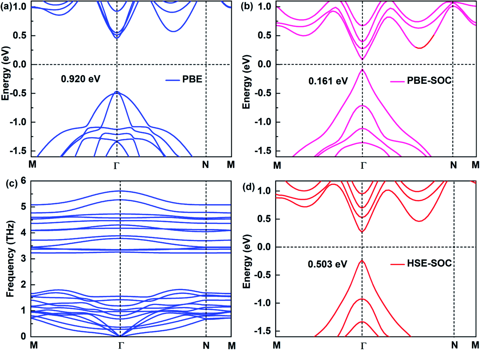
The electronic structure of 2D materials is crucial for their applications in the field of semiconductors, photodetectors and other fields. Here, we study the electronic structures of Sb2Bi2 LHS under PBE, PBE-SOC, HSE-SOC, which are shown in Fig. 2(a), (b) and (d), respectively. Comparing the band structures of Sb2Bi2 LHS under PBE and HSE, it is evident that PBE underestimates the energy gaps. However, comparing the high computational cost of HSE functional with the significance of SOC on the electronic structure of SbmBin LHS, it is reasonable to discard HSE functional for calculating the band structures of SbmBin LHS. Besides, the stability and experimental feasibility are essential for Sb2Bi2 LHS, therefore we examined its phonon dispersion spectra. Once Sb2Bi2 LHS is confirmed to be stable, the other LHS should also show excellent stability. The phonon dispersion spectrum of Sb2Bi2 LHS with zigzag interface is shown in Fig. 2(c). Generally, the appearance of soft modes in phonon calculations indicates that the structure is unstable. Here, no soft phonon modes are observed in the computed phonon dispersion spectrum of Sb2Bi2 LHS, which validates its kinetic stability. The stability of SbmBin LHS not only provides a good opportunity to investigate its properties, but also indicates the feasibility to experimentally synthesize it.
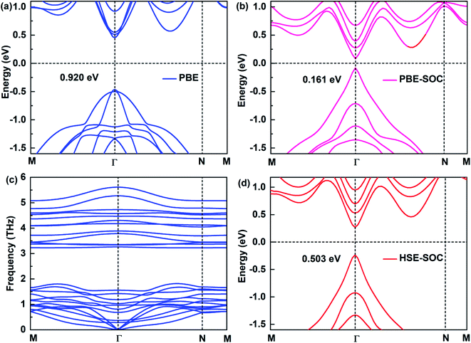 |
| | Fig. 2 Electronic structures of Sb2Bi2 LHS by using (a) PBE, (b) PBE-SOC, (d) HSE-SOC. (c) The phonon spectra is calculated to confirm the dynamic stability of the Sb2Bi2 LHS. | |
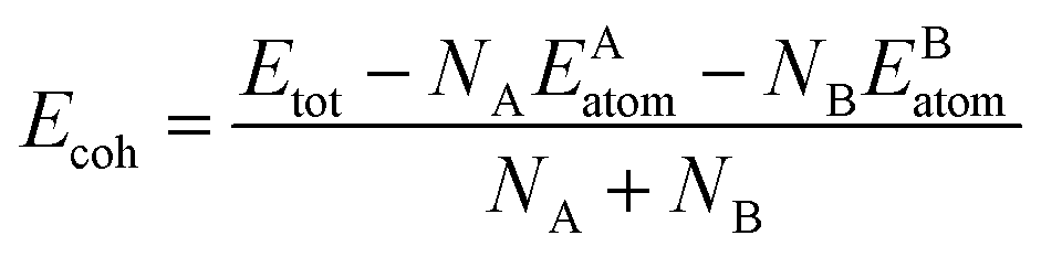
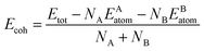
As we all know that the stabilities of nanomaterials are related to its cohesive energy, which is usually defined as the work when nanomaterials are decomposed into a single atom. Therefore, the cohesive energy per atom of SbmBin LHS can be calculated using eqn (1):49
| |
 | (1) |
where
Etot is the total energy of Sb
mBi
n LHS at the equilibrium states;
EAatom and
EBatom are the total energies of the isolated atoms Sb (−2.75 eV per atom) and Bi (−2.18 eV per atom) in the freedom states, respectively;
NA and
NB indicate respectively the total number of Sb and Bi atom in each unit cell. Therefore, the cohesive energy of Sb
mBi
n LHS is calculated about −1.55 eV per atom when
m and
n is different values.
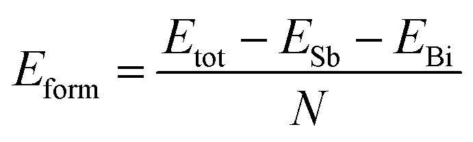
In order to verify the heterojunction formation abilities, we calculate formation energy. If the formation energy is negative, the formation of the heterojunction nanomaterials from its elements usually is an exothermic process. Therefore, the cohesive energy can be calculated using eqn (2):50
| |
 | (2) |
where
ESb solid and
EBi are the total energy of antimonene and bismuthene, respectively;
N denote the total atomic number of the system. Thus the formation energy of Sb
mBi
n LHS is calculated about −3.35 eV per atom. It is worth noting here that negative value means that the Sb
mBi
n LHS should be energetically favorable in experimental viability.
3.3 Work function and charge density analysis
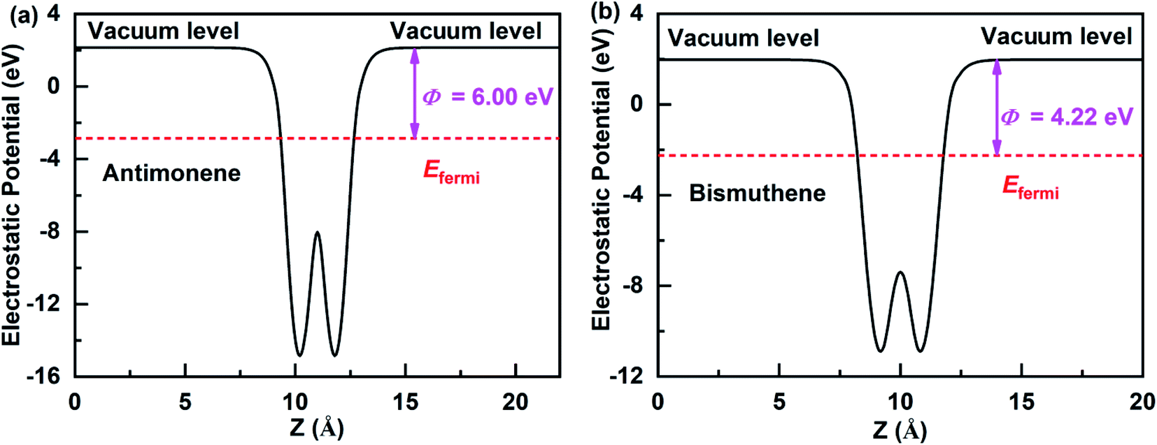
The work function is an important physical parameter in studying on the band alignment and charge transfer of semiconductor heterostructure. The work function is numerically equal to the difference between vacuum and Fermi levels and is expressed as follows:where Φ, Evac, and Efermi denote work function, vacuum level, and Fermi level, respectively. The work function of antimonene and bismuthene could be obtained by calculating the electrostatic potential of their slab models. Fig. 3(a) and (b) shows the electrostatic potential of antimonene and bismuthene are calculated using HSE hybrid functional with work function 6.00 eV and 4.22 eV, respectively. The work function of the bismuthene was less than that of the antimonene. As a result, when the bismuthene were interacted with the antimonene to form the SbmBin LHS, the electrons would flow from the bismuthene to the antimonene until they reached the same Fermi levels. The antimonene and bismuthene became charged because of the electron transfer and a built-in electric field was formed at their heterointerface. The direction of the electric field is from the bismuthene to the antimonene.
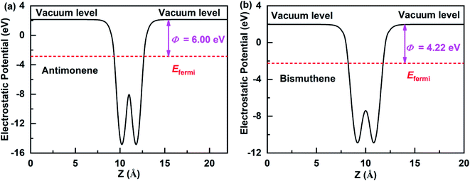 |
| | Fig. 3 Electrostatic potentials of the antimonene surface and bismuthene surface using HSE hybrid functional. | |
To further illustrate the charge transfer between antimonene and bismuthene, we have estimated the charge density difference of Sb8Bi8 LHS in detail. The charge density difference can be calculated as follows:
| | |
Δρ = ρtot − ρSb − ρBi
| (4) |
where
ρtot,
ρSb, and
ρBi denote the total charge densities of Sb
8Bi
8 LHS, monolayer antimonene and bismuthene nanosheet, respectively. The charge density difference of Sb
8Bi
8 LHS is illustrated in
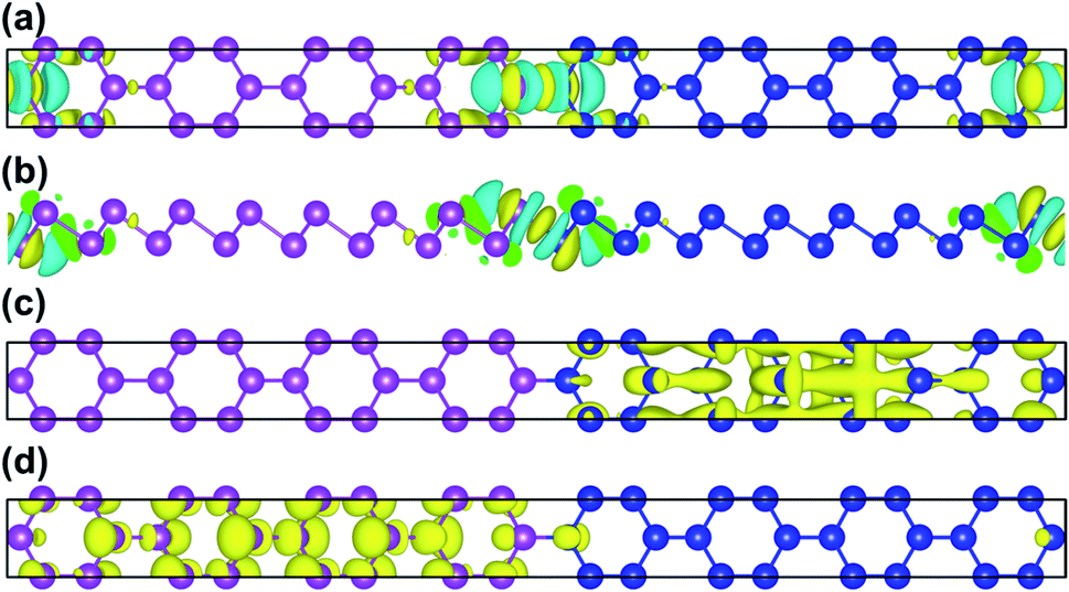
Fig. 4(a) and (b). The yellow area represents electron accumulation, and the cyan area shows the electron depletion. At the heterointerfaces of Sb
8Bi
8 LHS, the electron accumulation between Sb atom and Bi atom denote that a covalent bonding is formed. Besides, the calculated band decomposed charge density of the VBM and CBM is plotted in
Fig. 4(c) and (d). We can see that the VBM and CBM distribute on opposite sides of the heterointerfaces, verifying that Sb
mBi
n LHS is the type-II. The type-II band alignment could also be the reason for the transition from indirect to direct semiconductor.
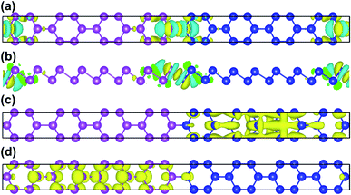 |
| | Fig. 4 (a) The top and (b) side views of charge density difference configurations of Sb8Bi8 LHS; (c) VBM and (d) CBM of Sb8Bi8 LHS for the band structure at the Γ-point, and positive and negative charges are represented in yellow and cyan, respectively. | |
3.4 Dirac cone and orbital-projected bands
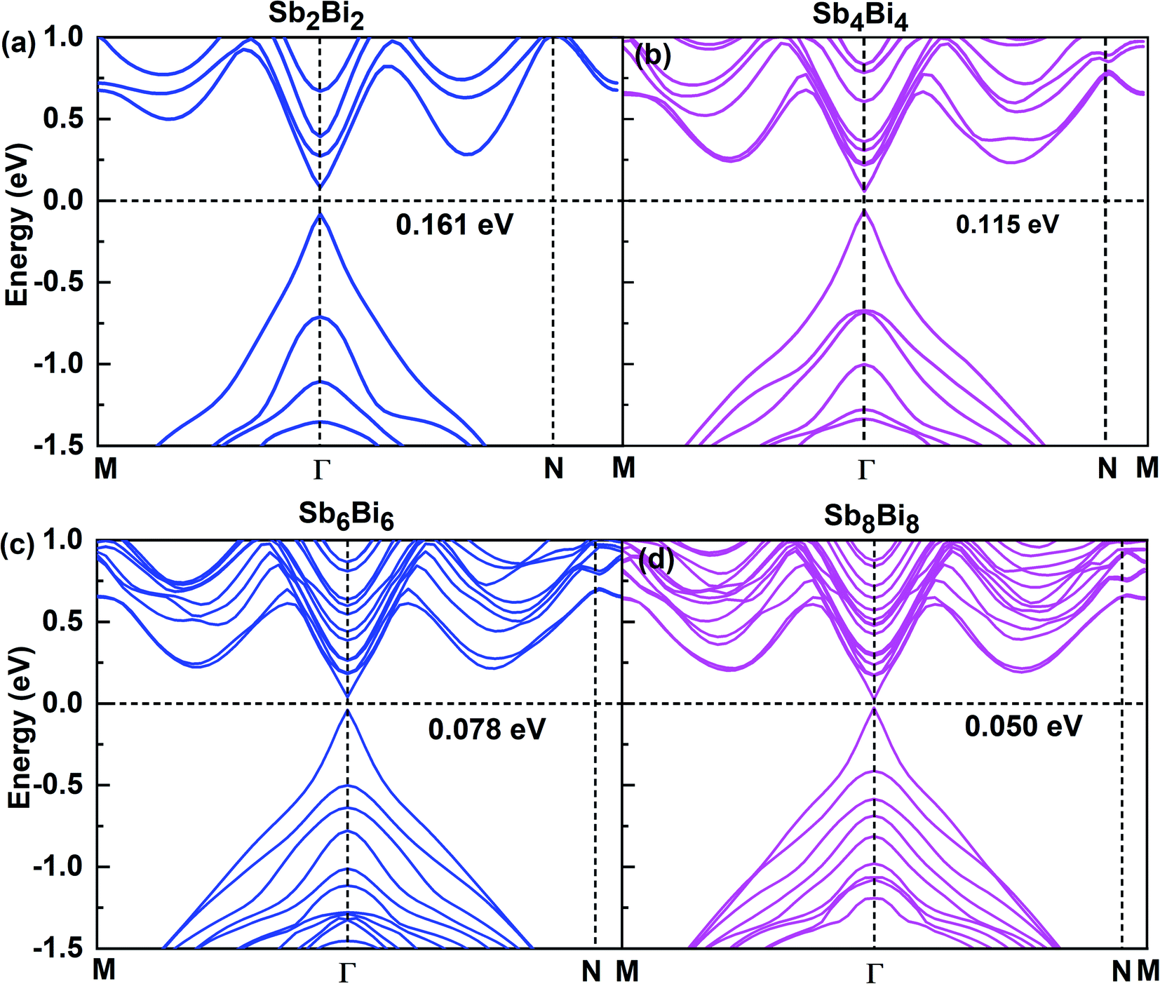
After confirming the structural stability of SbmBin LHS, we now focus on their electronic structure and optical properties. The electronic structures of SbmBin LHS (m = n) are shown in Fig. 5. Notably, the electronic structure transform from indirect band gap of the pristine structure (antimonene and bismuthene) to direct band gap of SbmBin LHS. Such a change is attributed to the fact that the lateral heterojunction destroys the pristine structural symmetry and built-in electric field in formed at the heterointerfaces. When m = n, SbmBin LHS are Dirac materials and their band gaps gradually decrease with their size increasing, which intrinsically corresponds to a semiconductor-to-semimetal transition. It is well known that Dirac materials have extraordinary properties and numerous potential applications, most of which are closely related to the ultra-high carrier mobility.51–53 In particular, the Dirac fermions in graphene lead to quantum Hall effect54 and ultra-high carrier mobility, which is as high as 2 × 105 cm2 V−1 s−1 at room temperature.55,56 Dirac materials, characterized by linear band dispersion at the Fermi level, are at the heart of several unconventional phenomena such as realization of extremely high free carrier mobility and quantum Hall effect, which indicates their immense potential for the development of nanoelectronic devices. Besides, type-II band alignment can be observed in SbmBin LHS because VBM state is mainly derived from antimonene and CBM from bismuthene. Further, similar results have been reported for the MoS2/WSe2 (ref. 57) LHS and As/Sb58 LHS. The above results open a new route toward the integration of Dirac physics, spintronics, and valleytronics.
 |
| | Fig. 5 Band structures for different atomic configurations of (a) Sb2Bi2 LHS, (b) Sb4Bi4 LHS, (c) Sb6Bi6 LHS and (d) Sb8Bi8 LHS using PBE + SOC method. | |
To investigate the band characteristics of SbmBin LHS, the orbital-projected band structures of Sb and Bi atoms in Sb8Bi8 LHS are displayed in Fig. 6(a) and (b), respectively. The size of red squares, purple diamonds and blue triangles represent the weights of px, py, pz orbitals of Sb atoms and Bi atoms of Sb8Bi8 LHS, respectively. It is clear from Fig. 6(a) and (b) that both VBM and CBM appear at the Γ point, resulting in a direct band gap of 0.05 eV according to DFT calculations. Because the s-orbital of Sb and Bi atoms is an inner orbital relative to p-orbital, it makes little contribution to the electronic structure near the Fermi level. Consequently, the p-orbital govern the electronic structure of SbmBin LHS near the Fermi level. Further analysis shows that the bonding states near VBM and CBM mainly originate from Bi-py orbitals (seen in Fig. 6(b)), while the Sb-p orbitals hardly impacts the electronic structure of the LHS (seen in Fig. 6(a)). Therefore, it is reasonable to ignore the effect of the orbitals of Sb atoms on the band structures of SbmBin LHS. These results provide useful insights on the electronic structure of SbmBin LHS.
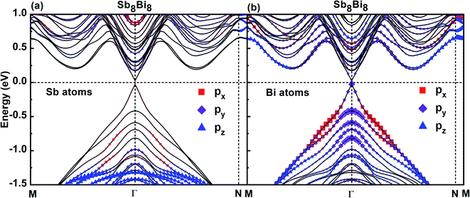 |
| | Fig. 6 Orbital-projected band structures of px, py, pz orbitals of Sb and Bi atoms of Sb8Bi8 LHS using PBE + SOC method. The size of red squares, purple diamonds and blue triangles represent the weights of px, py, pz orbitals, respectively. | |
3.5 Band structure and size dependence
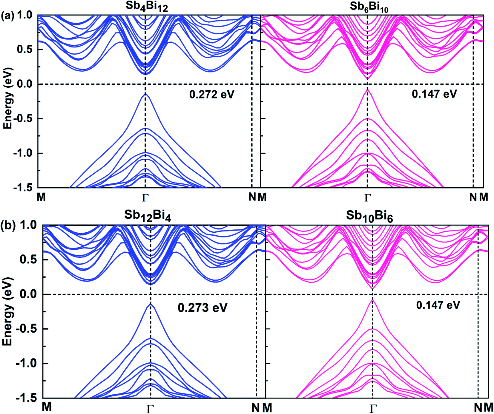
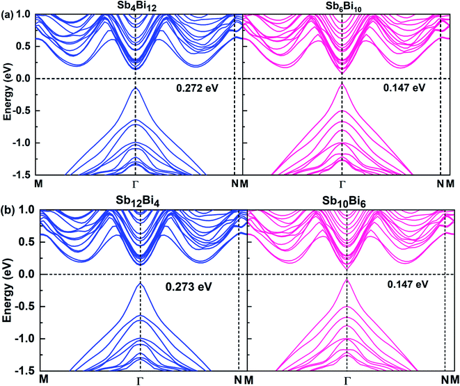
When m = n, we have confirmed that SbmBin LHS are Dirac materials with symmetric structures. When m ≠ n, SbmBin LHS including Sb4Bi12, Sb6Bi10, Sb10Bi6, and Sb12Bi4 are asymmetric structures and the corresponding electronic structures are shown in Fig. 7. All these LHS retain a recognizable direct band gap near the Fermi level. However, compared to the symmetric SbmBin LHS, the electronic structures of asymmetric Sb4Bi12 LHS and Sb12Bi4 LHS transform from Dirac semimetal to semiconductor. This is mainly because the built-in electric field at the heterointerfaces of the asymmetric structure changes the mechanism of electron transport. Thus, we have demonstrated that SbmBin LHS can maintain the Dirac semimetallic character only if the condition m ≈ n is satisfied, and the corresponding histogram is shown in Fig. 8(a). Besides, the band gaps of the SbmBin LHS exhibit size dependence, which is illustrated in Fig. 8(b). It is clear that the band gap of SbmBin LHS tends to zero when the size is larger than a critical value, which essentially corresponds to the transition from semiconductor to semimetal. We believe that these excellent properties of SbmBin LHS will inspire researchers to synthesize them.
 |
| | Fig. 7 Band structures of (a) Sb4Bi12 LHS (left) and Sb6Bi10 LHS (right), (b) Sb12Bi4 LHS (left) and Sb10B6 LHS (right) using PBE + SOC method. | |
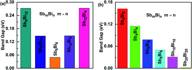 |
| | Fig. 8 Band alignments of (a) SbmBin LHS (m ≠ n), (b) SbmBin LHS (m = n). The band alignments of all systems belong to type II. | |
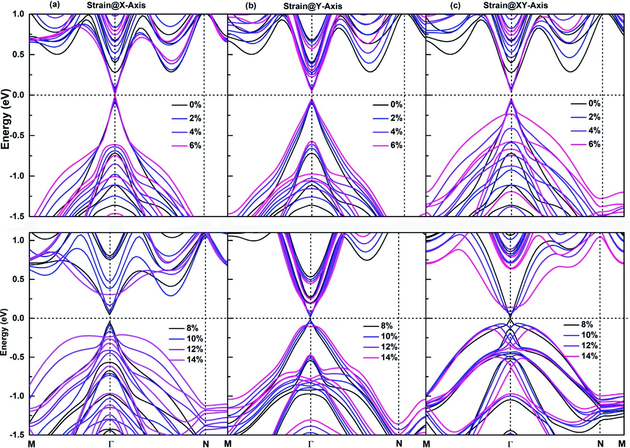
3.6 Strain dependence of LHS
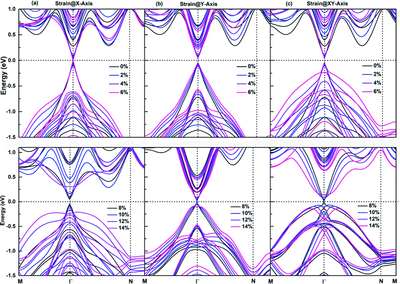
The application of an appropriate tensile strain is another effective method to tune the band structures of 2D materials, its effectiveness has been demonstrated on respectively. The size of red squares, purple diamonds and antimonene, which is an important member of SbmBin LHS. The antimonene can endure a large tensile strain up to 18%, and its band gap decreases with the tensile strain increasing,59 which causes the realization of QSHE. It is well established that for large tensile strain, the strong covalent interaction in the plane of LHS ensures their structural stability. As a result, SbmBin LHS can also endure large tensile strain. The strain dependence of the electronic structure of Sb2Bi2 LHS within 0–14% tensile strain is shown in Fig. 9. We have considered the tensile strain along three different directions: X-axis, Y-axis, and XY-axis. The analysis for the first case indicates that when the tensile strain is 0–6%, CBM and VBM are continuously shifted toward the Fermi level with the tensile strain increasing, resulting in band gap narrowing. When the tensile strain is greater than 6%, there is a Dirac cone near Fermi level. The application of strain@Y-axis and strain@XY-axis causes a similar response, which is illustrated in Fig. 9(b) and (c), respectively. Further, we observed that the electronic structures below the Fermi level significantly change with the tensile strain increasing. The electronic structures corresponding to the case of strain@XY-axis exhibit two separate strain dependences, but the influence of strain@X-axis is dominant. Nevertheless, it is worth noting that the band structure seems to be reversed when the tensile strain is applied along three different directions.
 |
| | Fig. 9 The strain dependence along three different directions of (a) X-axis, (b) Y-axis, and (c) XY-axis on the band structures of Sb2Bi2 LHS using PBE + SOC method. | |
According to Fig. 6, the bonding states near VBM and CBM mainly originate from Bi-py orbitals, while the Sb-p orbital character of bands hardly impact the electronic structure of SbmBin LHS. The orbital-projected band structures are suitable for investigating the strain dependence of the electronic structure of SbmBin LHS. The orbital-projected band structure for strain@X-axis of Sb2Bi2 LHS is illustrated in Fig. 10(a) and (b). It is clear that when the tensile strain reaches 2% (seen in Fig. 10(a)), the valence band near the Fermi level includes Bi-py orbitals. When the tensile strain reaches 6%, Sb2Bi2 LHS exhibits Dirac semimetallic properties and VBM and CBM touch each other. When the tensile strain is greater than 6% (seen in Fig. 10(b)), the contribution of the Bi-py orbitals stays in the conduction band. Afterwards, the band gaps increase gradually with the tensile strain increasing and the band inversion occurs near Γ point. Similarly, the orbital-projected band structures for strain@Y-axis and strain@XY-axis of Sb2Bi2 LHS exhibit band inversion at the Γ point, which is illustrated in ESI, Fig. S1 and S2.† However, the difference between the two cases is that the contribution of the Bi-px orbitals and Bi-pz orbitals stays in the conduction band when the tensile strain is applied along the Y-axis and XY-axis, respectively. The band inversion indicates that SbmBin LHS are promising to realize QSHE.
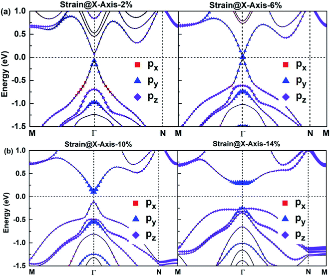 |
| | Fig. 10 The orbital-projected band structures of strain@X-axis of Bi atoms of Sb2Bi2 LHS using PBE + SOC method. The size of red squares, purple diamonds and blue triangles represent the weights of px, py, pz orbitals, respectively. | |
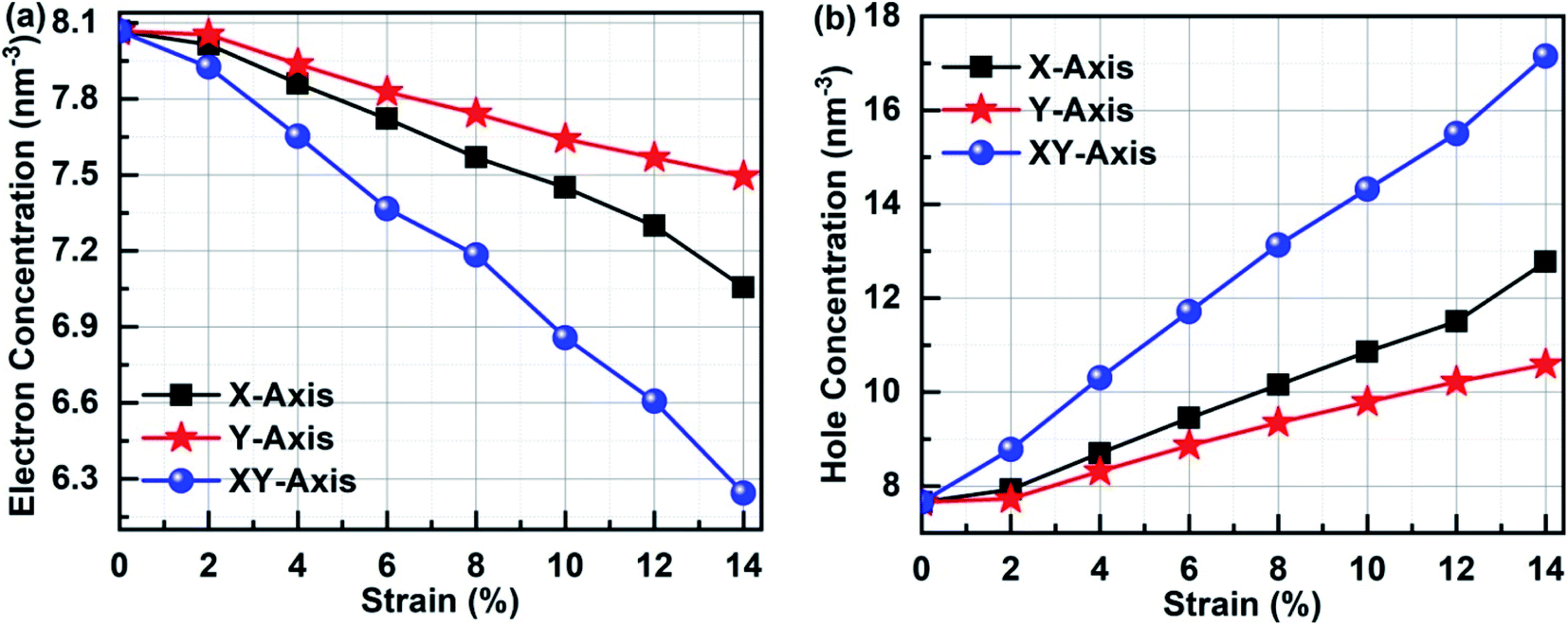
3.7 The concentration analysis
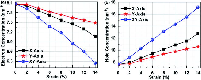
In order to clarify the relationship between the electronic performances of Sb2Bi2 LHS and the tensile strain, we have calculated the concentration of the electron and hole in different tensile strain, which is illustrated in Fig. 11. The electron concentration of all lateral heterojunctions remain a value with 7.66 nm−3 and that of the hole concentration remain a value with 8.07 nm−3, when the SbmBn LHS are not subjected to tensile strain in any direction. However, once the SbmBin LHS is subjected to tensile strain with different direction, the electrons in the valence band transfer to the conduction band. With the increase of tensile strain, the electron concentration decreases (seen in Fig. 11(a)), but the hole concentration increases (seen in Fig. 11(b)), because the total number of the electron and hole does not varies with the tensile strain. On the other hand, the variation relationship of the electron concentration and the hole concentration is XY-axis > X-axis > Y-axis, denoting that there are more the electron hole pair in Sb2Bi2 LHS in XY-axis strain than X-axis and Y-axis strain.
 |
| | Fig. 11 (a) Electron concentration and (b) hole concentration of Sb2Bi2 LHS in the tensile strain with different direction. | |
4. Conclusions
In this review, we systematically investigate SbmBin LHS and found that an abrupt transition from indirect-band gap of the antimonene and bismuthene to direct-band gap of SbmBin LHS is observed. SbmBin LHS exhibit a type-II band alignment, which is potentially useful for future photoelectronics. Additionally, the size of SbmBin LHS is observed to be a key parameter that governed their electronic structures and optical properties. The band gaps of SbmBin LHS tend to zero when their size is larger than the critical value, which essentially corresponds to a transition from semiconductor to semimetal. Besides, the tensile strain accelerate the electrons in the valence band transfer to the conduction band, leading to the electron concentration decreases and the hole concentration increases with tensile strain increases. The band inversion near Γ point occurs on suitable strain, indicating that SbmBin LHS are very promising to realize QSHE. These fascinating electronic and optical properties make it extensively used in the fields of electronics, optoelectronics and other fields.
Conflicts of interest
The authors declare there is no conflicts of interest regarding the publication of this paper.
Acknowledgements
This research was supported by Doctoral Scientific Research Foundation of East China University of Technology (Grant No. DHBK2019256).
References
- H. Morkoc and S. N. Mohammad, Science, 1995, 267, 51–55 CrossRef CAS PubMed.
- T. Mimura, S. Hiyamizu, T. Fujii and K. Nanbu, JPN. J. Appl. Phys., 1980, 19, L225 CrossRef CAS.
- D.-R. Chen, M. Hofmann, H.-M. Yao, S.-K. Chiu, S.-H. Chen, Y.-R. Luo, C.-C. Hsu and Y.-P. Hsieh, ACS Appl. Mater. Inter., 2019, 11, 6384–6388 CrossRef CAS PubMed.
- Y. Zhan, Z. Shao, T. Jiang, J. Ye, X. Wu, B. Zhang, K. Ding, D. Wu and J. Jie, J. Mater. Chem. A, 2020, 8, 789–796 RSC.
- Q. Tong, H. Yu, Q. Zhu, Y. Wang, X. Xu and W. Yao, Nat. Phys., 2017, 13, 356–362 Search PubMed.
- A. K. Geim and I. V. Grigorieva, Nature, 2013, 499, 419 CrossRef CAS PubMed.
- S.-C. Lu, M. Mohamed and W. Zhu, 2D Mater., 2016, 3, 011010 CrossRef.
- M. M. Furchi, A. Pospischil, F. Libisch, J. Burgdörfer and T. Mueller, Nano Lett., 2014, 14, 4785–4791 CrossRef CAS.
- B. Zheng, C. Ma, D. Li, J. Lan, Z. Zhang, X. Sun, W. Zheng, T. Yang, C. Zhu and G. Ouyang, J. Am. Chem. Soc., 2018, 140, 11193–11197 CrossRef CAS PubMed.
- Z. Zhang, P. Chen, X. Duan, K. Zang, J. Luo and X. Duan, Science, 2017, 357, 788–792 CrossRef CAS PubMed.
- L. Liu, J. Park, D. A. Siegel, K. F. McCarty, K. W. Clark, W. Deng, L. Basile, J. C. Idrobo, A.-P. Li and G. Gu, Science, 2014, 343, 163–167 CrossRef CAS PubMed.
- Y. Gong, J. Lin, X. Wang, G. Shi, S. Lei, Z. Lin, X. Zou, G. Ye, R. Vajtai and B. I. Yakobson, Nature Mater, 2014, 13, 1135 CrossRef CAS PubMed.
- M.-Y. Li, Y. Shi, C.-C. Cheng, L.-S. Lu, Y.-C. Lin, H.-L. Tang, M.-L. Tsai, C.-W. Chu, K.-H. Wei and J.-H. He, Science, 2015, 349, 524–528 CrossRef CAS.
- C. Huang, S. Wu, A. M. Sanchez, J. J. Peters, R. Beanland, J. S. Ross, P. Rivera, W. Yao, D. H. Cobden and X. Xu, Nat. Mater., 2014, 13, 1096 CrossRef CAS PubMed.
- M. Mahjouri-Samani, M.-W. Lin, K. Wang, A. R. Lupini, J. Lee, L. Basile, A. Boulesbaa, C. M. Rouleau, A. A. Puretzky and I. N. Ivanov, Nat. Commun., 2015, 6, 1–6 Search PubMed.
- E. G. Marin, D. Marian, M. Perucchini, G. Fiori and G. Iannaccone, ACS Nano, 2020, 14, 1982–1989 CrossRef CAS PubMed.
- T. Habe, J. Appl. Phys., 2019, 126, 123901 CrossRef.
- Y. Deng, Z. Luo, N. J. Conrad, H. Liu, Y. Gong, S. Najmaei, P. M. Ajayan, J. Lou, X. Xu and P. D. Ye, ACS Nano, 2014, 8, 8292–8299 CrossRef CAS PubMed.
- X. Duan, C. Wang, J. C. Shaw, R. Cheng, Y. Chen, H. Li, X. Wu, Y. Tang, Q. Zhang and A. Pan, Nat. Nanotechnol., 2014, 9, 1024 CrossRef CAS.
- W. Hong, G. W. Shim, S. Y. Yang, D. Y. Jung and S. Y. Choi, Adv. Funct. Mater., 2019, 29, 1807550 CrossRef.
- M. Liu, Y. Li, P. Chen, J. Sun, D. Ma, Q. Li, T. Gao, Y. Gao, Z. Cheng and X. Qiu, Nano Lett., 2014, 14, 6342–6347 CrossRef CAS PubMed.
- K. Chen, X. Wan, W. Xie, J. Wen, Z. Kang, X. Zeng, H. Chen and J. Xu, Adv. Mater., 2015, 27, 6431–6437 CrossRef CAS PubMed.
- X.-Q. Zhang, C.-H. Lin, Y.-W. Tseng, K.-H. Huang and Y.-H. Lee, Nano Lett., 2014, 15, 410–415 CrossRef PubMed.
- Y. Liu, M. Bo, X. Yang, P. Zhang, C. Q. Sun and Y. Huang, Phys. Chem. Chem. Phys., 2017, 19, 5304–5309 RSC.
- S. Wang, X. Zhang, Y. Huang and C. Q. Sun, Phys. Chem. Chem. Phys., 2018, 20, 25716–25721 RSC.
- Z. Liu, W. Feng, H. Xin, Y. Gao, P. Liu, Y. Yao, H. Weng and J. Zhao, Mater. Horiz., 2019, 6, 781–787 RSC.
- X. Liu, S. Zhang, S. Guo, B. Cai, S. A. Yang, F. Shan, M. Pumera and H. Zeng, Chem. Soc. Rev., 2020, 49, 263–285 RSC.
- W. Jang, K. Kang and A. Soon, Nanoscale, 2016, 8, 14778–14784 RSC.
- T. Hu, H. Wu, H. Zeng, K. Deng and E. Kan, Nano Lett., 2016, 16, 8015–8020 CrossRef CAS PubMed.
- J. Pei, X. Gai, J. Yang, X. Wang and Y. Lu, Nat. Commun., 2016, 7, 10450 CrossRef CAS PubMed.
- J. Zhao, K. Cheng, N. Han and J. Zhang, WIRES. Comput. Mol. Sci., 2018, 8, e1353 CrossRef.
- S. Zhang, S. Guo, Z. Chen, Y. Wang, H. Gao, J. Gómez-Herrero, P. Ares, F. Zamora, Z. Zhu and H. Zeng, Chem. Soc. Rev., 2018, 47, 982–1021 RSC.
- J. Ji, X. Song, J. Liu, Z. Yan, C. Huo, S. Zhang, M. Su, L. Liao, W. Wang and Z. Ni, Nat. Commun., 2016, 7, 13352 CrossRef CAS PubMed.
- F. Reis, G. Li, L. Dudy, M. Bauernfeind, S. Glass, W. Hanke, R. Thomale, J. Schäfer and R. Claessen, Science, 2017, 357, 287–290 CrossRef CAS PubMed.
- S. Zhang, Z. Yan, Y. Li, Z. Chen and H. Zeng, Angew. Chem., Int. Ed., 2015, 54, 3112–3115 CrossRef CAS PubMed.
- G. Wang, R. Pandey and S. P. Karna, ACS Appl. Mater. Inter., 2015, 7, 11490–11496 CrossRef CAS PubMed.
- E. Aktürk, O. Ü. Aktürk and S. Ciraci, Phys. Rev. B, 2016, 94, 014115 CrossRef.
- X. Wang, C. Xu, H. Hu, P. Wang, G. Bian, W. Tan, S. Brown and T.-C. Chiang, EPL, 2017, 119, 27002 CrossRef.
- Y. Guo, F. Pan, M. Ye, X. Sun, Y. Wang, J. Li, X. Zhang, H. Zhang, Y. Pan and Z. Song, ACS Appl. Mater. Inter., 2017, 9, 23128–23140 CrossRef CAS PubMed.
- F.-C. Chuang, C.-H. Hsu, C.-Y. Chen, Z.-Q. Huang, V. Ozolins, H. Lin and A. Bansil, Appl. Phys. Lett., 2013, 102, 022424 CrossRef.
- T. Zhou, J. Zhang, Y. Xue, B. Zhao, H. Zhang, H. Jiang and Z. Yang, Phys. Rev. B, 2016, 94, 235449 CrossRef.
- H. Jin, V. Michaud-Rioux, Z.-R. Gong, L. Wan, Y. Wei and H. Guo, J. Mater. Chem. C, 2019, 7, 3837–3842 RSC.
- G. Kresse and J. Furthmüller, Comp. Mater. Sci., 1996, 6, 50 Search PubMed.
- G. Kresse, Phys. Rev. B: Condens. Matter Mater. Phys., 1996, 54, 11169–11186 CrossRef CAS PubMed.
- J. P. Perdew, K. Burke and M. Ernzerhof, Phys. Rev. Lett., 1996, 77, 3865 CrossRef CAS PubMed.
- S. Grimme, J. Antony, S. Ehrlich and H. Krieg, J. Chem. Phys., 2010, 132, 154104 CrossRef PubMed.
- J. Paier, M. Marsman, K. Hummer, G. Kresse, I. C. Gerber and J. G. Ángyán, J. Chem. Phys., 2006, 124, 154709 CrossRef CAS PubMed.
- S. Silver, J. Yin, H. Li, J. L. Brédas and A. Kahn, Adv. Energy Mater., 2020, 10, 2000390 CrossRef CAS.
- L. M. Dong, Z. D. Han, Y. Z. Guan, W. Li and X. Y. Zhang, Mat. Sci. Eng. R, 2012, 545, 13–19 CrossRef CAS.
- Q. Sun, Y. Dai, N. Yin, L. Yu, Y. Ma, W. Wei and B. Huang, Nano Res., 2017, 10, 3909–3919 CrossRef CAS.
- J. Wang, S. Deng, Z. Liu and Z. Liu, Nat. Sci. Rev., 2015, 2, 22–39 CrossRef CAS.
- Y. Zhang, Y.-W. Tan, H. L. Stormer and P. Kim, Nature, 2005, 438, 201–204 CrossRef CAS PubMed.
- W. Li, M. Guo, G. Zhang and Y.-W. Zhang, Phys. Rev. B: Condens. Matter Mater. Phys., 2014, 89, 205402 CrossRef.
- C. R. Dean, L. Wang, P. Maher, C. Forsythe, F. Ghahari, Y. Gao, J. Katoch, M. Ishigami, P. Moon and M. Koshino, Nature, 2013, 497, 598–602 CrossRef CAS PubMed.
- S. Morozov, K. Novoselov, M. Katsnelson, F. Schedin, D. Elias, J. A. Jaszczak and A. Geim, Phys. Rev. Lett., 2008, 100, 016602 CrossRef CAS PubMed.
- K. I. Bolotin, K. J. Sikes, Z. Jiang, M. Klima, G. Fudenberg, J. Hone, P. Kim and H. Stormer, Solid State Commun., 2008, 146, 351–355 CrossRef CAS.
- M.-H. Chiu, C. Zhang, H.-W. Shiu, C.-P. Chuu, C.-H. Chen, C.-Y. S. Chang, C.-H. Chen, M.-Y. Chou, C.-K. Shih and L.-J. Li, Nat. Commun., 2015, 6, 1–6 Search PubMed.
- Q. Sun, Y. Dai, Y. Ma, N. Yin, W. Wei, L. Yu and B. Huang, 2D Mater., 2016, 3, 035017 CrossRef.
- M. Zhao, X. Zhang and L. Li, Sci. Rep., 2015, 5, 16108 CrossRef PubMed.
Footnote |
| † Electronic supplementary information (ESI) available. See DOI: 10.1039/d1ra02702f |
|
| This journal is © The Royal Society of Chemistry 2021 |
Click here to see how this site uses Cookies. View our privacy policy here. 
 Open Access Article
 This Open Access Article is licensed under a Creative Commons Attribution-Non Commercial 3.0 Unported Licence
 ab
ab