
 Open Access Article
 This Open Access Article is licensed under a Creative Commons Attribution-Non Commercial 3.0 Unported Licence
Off-axis microsphere photolithography patterned nanohole array and other structures on an optical fiber tip for glucose sensing
Jiayu Liu†
 a,
Ibrahem Jasim†a,
Tao Liuc,
Jie Huangc,
Edward Kinzelb and
Mahmoud Almasri*a
a,
Ibrahem Jasim†a,
Tao Liuc,
Jie Huangc,
Edward Kinzelb and
Mahmoud Almasri*a
aDepartment of Electrical Engineering and Computer Science, University of Missouri, Columbia, Missouri 65211, USA. E-mail: almasrim@missouri.edu
bDepartment of Mechanical and Aerospace Engineering, University of Notre Dame, Notre Dame, Indiana 46556, USA
cDepartment of Electrical and Computer Engineering, Missouri University of Science and Technology, Rolla, Missouri 47906, USA
First published on 28th July 2021
Abstract
Microsphere photolithography (MPL) using off-axis UV exposure is a technique that uses a layer of self-assembled microspheres as an optical mask to project different periodic nanopatterns. This paper introduces MPL as an alternative fabrication technique to pattern complex metasurfaces on an optical single mode fiber tip as a sensor for measuring refractive index. Based on the hexagonal close packing microsphere array, complicated metasurfaces were successfully created by changing the UV illumination angle. Using the same self-assembled microspheres monolayer, multiple UV illumination jets were projected to create multiple hole group patterns. Fiber sensors with three-hole group and four-hole group patterns were fabricated and tested with different glucose concentrations in water. The different concentration solutions have various refractive indexes, which result in the shift of the metasurface resonant wavelength, represented as sensitivity. The testing results show that the three-hole group and four-hole group have the sensitivity of 906 nm per RIU and 675 nm per RIU, respectively. Finite element analysis was used to model the fiber sensor's surrounding with different refractive index solutions. These new pattern metasurface coated fibers' refractive index sensitivity has increased by 40% compared to our previous work, while the technique still provides a cost-effective, flexible, high-throughput fabrication of the fiber sensor.
Introduction
Sensors in a small scale have been used widely in many applications such as physical, medical and biochemical sensing. Miniature sensors can be realized and built in a micro/nano scale due to the recent advances in micro and nano fabrication.1 Localized Surface Plasmon Resonance (LSPR) has attracted many miniature sensor researcher's attentions in recent years. LSPR can be excited when an electromagnetic wave incidents on the interface of the metal and the dielectric, and can propagate along the interface which generates surface plasmon polaritons (SPPs).2 Miniature sensors have been using the SPR technique for the detection of chemical species when paired with reagents.3 The plasmonic sensing material can be either metal4–7 or dielectric8–11 which produce different resonant wavelengths dependent on their refractive indexes and geometry structures.A nanostructure with surface plasmon resonance was used for the detection of low concentrations of glucose in water. The nanostructure was fabricated on a glass substrate using electron beam lithography.12 The sensor was performed by utilizing nanohole arrays in a gold thin layer and tested with different fluids to show the response of the sensor under different refractive index conditions.
Due to their smaller sizes, flexibility, extreme light weight, immunity to electromagnetic interference, remote sensing ability, high local selectivity, low cost and high sensitivity, the optical fiber sensors have been widely studied and developed.13 They were used in a wide spectrum of sensing applications such as biological,14 gas15 and chemical.16 While many examples are on planar substrates, several groups have realized patterning on fibers. Fiber optic plasmonic sensors were fabricated with sensing pattern material patterned either on the sidewall of the fiber probe,17–19 tip of the fiber20–28 or both.28,29 Nano disks pattern on a fiber optic tip was used for the detection of a cancer protein biomarker.30 An e-beam lithography technique was used to create periodic chromium–gold nano disks integrated with a feedback loop to act on the optical gain element and translate it to impedance matching. The detection limit was 10−5 RIU 31. Extraordinary Optical Transmission (EOT) reflection – based fiber optic was implemented for the identification of chemical substances. The sensing goal can be achieved by fabricating subwavelength hole arrays on metal thin film coated at the optical fiber tip. If the refractive index of the surrounding medium increases, the spectrum shifts to longer wavelength. The single mode fiber optic sensor was developed to work in the near infrared wavelength spectrum by carefully choosing the hole arrays orientations. The near infrared region includes plenty of information from abundant sources and for detectors. The patterned holes on fiber tips were fabricated using the E-beam or focused ion beam (FIB) techniques.32 The fabricated sensor showed a high sensitivity for different concentrations of salt in water.33 However, the disadvantages of the available SPR based chemical sensing methods are the complexity and the high cost of E-beam lithography fabrication for disposable sensors.32–34
New techniques that use microspheres have been recently used in micromachining. The use of microspheres has several advantages such as, easy to handle, cost effective, no need for complex alignment or masks and ability to fabricate nano-scale structures. Polystyrene (PS) nanospheres were used to create gold nanotips on the end face of the optical fiber. The implemented nano structures using this method are limited because the fabrication process is only dependent on the nanospheres and their size.35,36 Triangular shaped gold nanostructures were fabricated on the tip of fiber optic using microbeads which is a cheap colloidal lithography technique.37 Those methods can create small patterns but lack geometric flexibility. Instead, microspheres can be used as optical mask to create different patterns on photoresist layer.
Recently, multiple groups achieved steering of photonic nanojet around by tilting the substrate under the UV radiation,38–40 or by controlling the illumination angle by using a fourier mask.41 Deep UV illumination was used by Zhang et al.38 for patterning nanostructures to enhance the emission from LEDs, and by Guo et al.42 to pattern 370 nm wide trench in SbTe thin film using SiO2 microspheres and KrF excimer laser. However, all these relevant applications are still being designed based on silicon and metal substrate or platform that has a big surface area. However, this manuscript utilizes off-axis technique to pattern the metasurface on a small surface area such as single-mode fiber tip, which could potentially result in unexpected difficulties compared to the patterning fabrication on a large surface area such as glass slide.
This manuscript presents a low-cost fabrication of plasmonic sensors on the tip of a single mode optic fiber, using innovative off-axis microsphere photolithography (MPL). The periodic hole patterns were fabricated in an Al film coated on the fiber's tip. A self-assembled lattice of microspheres is used as an optical mask to pattern the periodic holes on a photoresist layer covered fiber tip by focusing the illumination light at a certain angle. Then the pattern was transfer to the Al layer by etching. Different periodic hole patterns metasurfaces have been successfully created using the off-axis MPL. The fabricated sensors were tested in various glucose concentrations in water and compared to simulation results.
Methods
MPL patterning process
A single mode fiber with cladding and core diameters of 125 μm and 8.2 μm, respectively, was used in this project. Due to the small surface area of the fiber end-face which can lead to a surface tension and eventually will ruin the pattern on the fiber tip, 125 μm inner diameter ceramic ferrule was used to hold the fiber. The initial step is to attach the fiber to the ferrule which was done by cutting the single mode fiber to 10 cm pieces. The jacket of first 1.5 cm of each piece end was removed by a stripper so it can be inserted inside the ferrule. Before the fiber was placed inside the ferrule, a small amount of glue was injected inside the ferrule. After we inserted the fiber head into the ferrule until we see the fiber tip from the end-face of the ferrule, we placed the ferrule on top of hot plate at 100 °C for 10 minutes for baking. Then, the fiber tip with the ferrule was polished and cleaned to achieve a clean and smooth fiber end surface. The fiber ferrule assembly was then sputter coated with 50 nm thick aluminum. A small 3D printed chunk was designed to hold the ferrule with the fiber for the following spin coating processing step. The ferrule was inserted into the chuck and was placed on the spin coater and spin coated with diluted Shipley 1805 photoresist (120 nm). After spin coating, the ferrule was removed from the chuck and transferred to a rack and placed in a beaker full of water for spheres coating. Then the sphere layer was assembled on the surface of the water by injecting 5 μl of the sphere butanol mixture on water surface. Once the butanol is contacted with water, it spreads quickly due to different surface tension compared to water, which assures that the spheres form only single layer. Then capillary force between spheres would drag them towards each other and form a close packed layer. After the layer was stabilized, the water was sucked out slowly. Eventually the spheres are coated on the top of the ferrule and the fiber. The sphere layer will go down as draining the water and finally the layer will sit on top of the ferrule along with the fiber. The fiber was then transferred to UV light source for photoresist patterning. Following by either metal etching through to form hole-pattern, or metal deposition and lift-off process for disk-pattern.The device was designed and fabricated to perform chemical sensing of different surrounding liquids. The device was tested by performing glucose concentration measurement. To achieve the required goal, thin film Al layer perforated with nano holes was implemented on top of a single mode fiber in an EOT configuration based on the refractive index change at the fiber/liquid interface. Fig. 1(a) shows a 3D schematic of the fiber tip thin layer packed with array of nano holes with the controlled angle and (b) the actual setup that helps control the UV incident angle. The mechanical stages shown in Fig. 1 are from Thorlabs. Finite Element Analysis Software Ansoft HFSS was employed to investigate the coupled modes stimulated by a plane wave propagating through the periodic hole array at single mode fiber end-face.
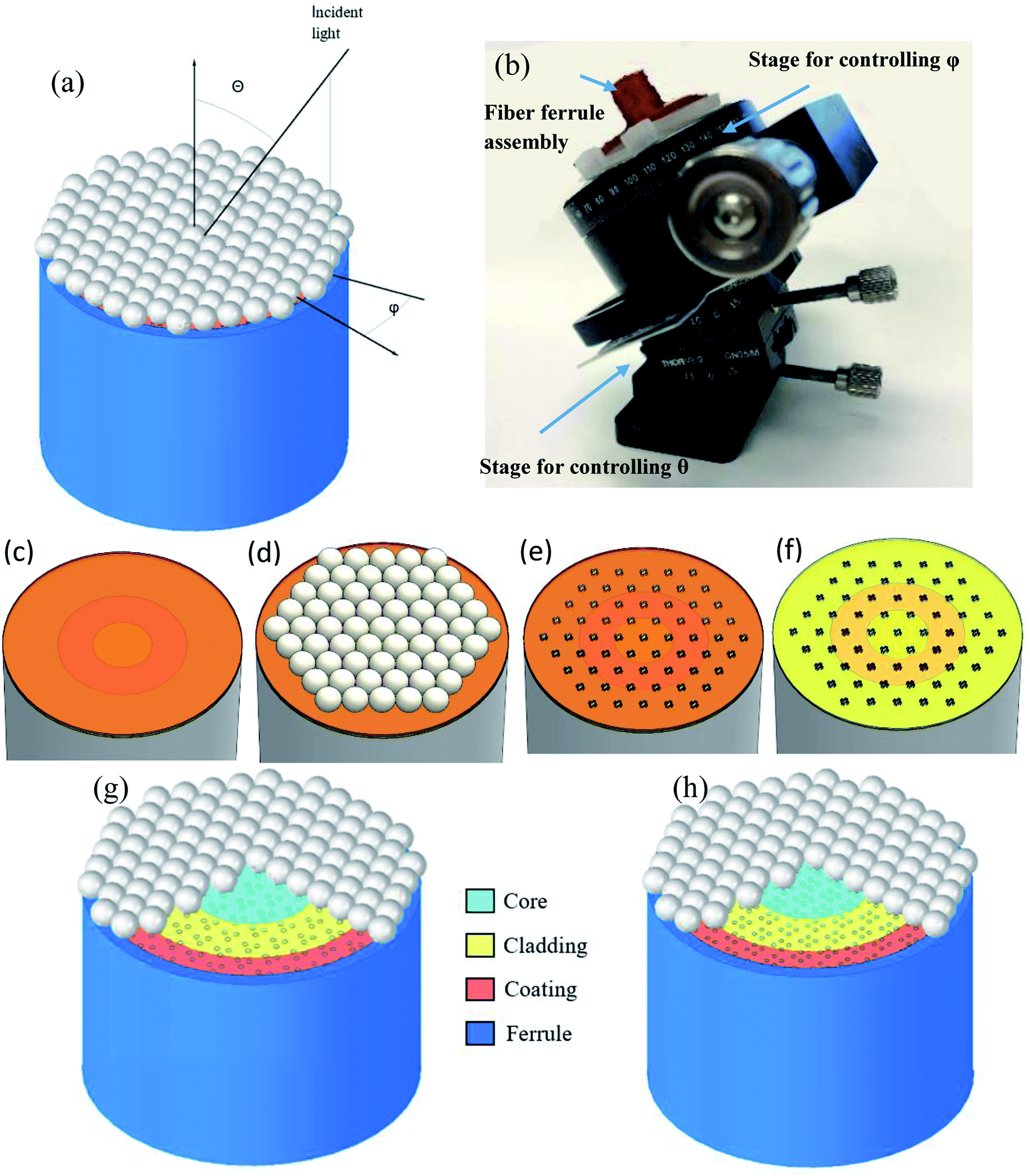 | ||
| Fig. 1 (a) Microspheres are self-assembled on top of the fiber surface will be exposed to UV light with controlled polar angle θ and azimuthal angel φ. (b) The stage used to help control the incident angle φ and θ. The top stage for φ is mounted on top of the stage for θ. The fiber ferrule assembly is fixed on the surface of the stage for φ. Schematic of the fabrication process for hole pattern: (c) thin film of Al and photoresist on the ferrule which includes the fiber tip in the center (core and cladding). (d) Microspheres assembly on top of the fiber tip. (e) Patterned photoresist by microspheres and (f) pattern transferred from photoresist to Al by metal etching on fiber core and cladding (yellow) and ferrule (gray). A schematic shows the sensor which includes microsphere array as an optical element on the fiber tip the fiber with the cladding and core were embedded into a ceramic ferrule. Holes patterns with (g) three holes and (h) four holes were created on metal layer. | ||
Fabrication of multiple nano structures, by utilizing off-axis UV exposure, have been created on the single mode fiber tip. Fig. 1c–f shows a schematic of the fabrication on the fiber tip step by step. First, a thin layer of photoresist was spincoated on the fiber tip which had a layer of Al layer on already. Then the fiber was transferred to 3D printed rack for sphere self-assembly. After sphere assembly, the fiber would be UV exposed and followed by developing to create patterns on the photoresist layer. Then the pattern was transferred from the photoresist layer to Al layer by metal etching through. The hole diameter could be manipulated by tuning the exposure dosage, while the hole depth depends on the pre-sputtered Al layer thickness. After the Al film was patterned, the fiber would be cleaned using acetone. Microspheres are self-assembled onto the photoresist layer on the fiber tip surface. After excess solvent were evaporated, the fiber along with the chuck were mounted to an optical stage and exposed to UV light at an angel measured from the surface: polar angle (θ) and azimuthal angel (φ) which can be controlled by tilting the stage. Each microsphere can focus the UV light into a photonic jet into the thin photoresist layer. The angle of the photonic jet was controlled by the stage. Fig. 1(g) and (h) shows an example of three-holes group and four-holes group by controlling θ and φ during UV exposure. UV exposure at different combination of θ and φ will create different nanostructures for desired optical applications. The range of θ and φ are from −30 to 30, and 0 to 360, respectively.
Different combination of polar angle (θ), azimuthal angel (φ), sphere and exposure dose determine the shape and the size of the nano structure created. Fiber mounted on the rotational stage that can control the angles were placed under UV source and exposed with controlled/certain amount of dose, followed by Al etching (50 nm thick) or deposition to create different structures (holes and disks). Fig. 2 shows the SEM of multi-holes group structures using off-axis exposure with different controlled parameters: (a) the fiber inside the ferrule. (b) 3 holes group: 3 exposures with θ = 30; φ = 0, 120, 240. (c) 4 holes group: 4 exposures with θ = 30; φ = 0, 90, 180, 270. (d) 5 holes group: 5 exposures with θ = 30; φ = 0, 72, 144, 216, 288; and SEM of more complicated structures and letters using off-axis exposure with different controlled parameters by Al lift-off. Al deposition and lift-off process step: (e) split ring or letter C patterned by Al deposition and lift-off: 12 exposures with θ = 30; v = 0–240 for every 20. (f) Rod by Al deposition and lift-off process: 4 exposures with θ = 30, 10, −30, −10; φ = 180, (g) continuous line by Al deposition and lift-off process, the fabrication step is the same to (f), but the line pattern is from the different orientation of the sphere. (h) Triploid by Al etching: 6 exposures with θ = 30, 10; φ = 0, 120, 240. (i) Letter V by Al deposition, (j) letter L by Al etching: 12 exposures with θ = 30; φ = 0–240 for every 20. (k) Letter T by Al deposition: 4 exposures with θ = 30, 10, −30, −10; φ = 180, (l) Letter X by Al deposition: 4 exposures with θ = 30, 10, −30, −10; φ = 180.
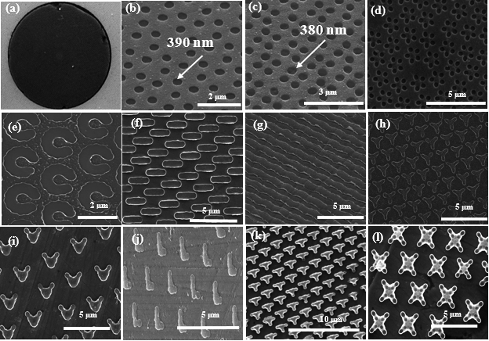 | ||
| Fig. 2 The SEM of holes group structures using off-axis exposure with different controlled parameters: (a) the fiber inside the ferrule. (b) 3 holes group: 3 exposures with θ = 30; φ = 0, 120, 240. (c) 4 holes group: 4 exposures with θ = 30; φ = 0, 90, 180, 270. (d) 5 holes group: 5 exposures with θ = 30; φ = 0, 72, 144, 216, 288. Structures and letters using off-axis exposure with different controlled parameters: (e) split ring or letter C by Al etching: 12 exposures with θ = 30; φ = 0–240 for every 20. (f) Rod by Al deposition: 4 exposures with θ = 30, 10, −30, −10; φ = 180, (g) continuous line by Al deposition, the fabrication step is the same to (f), but the line pattern is from the different orientation of the sphere. (h) Triploid by Al etching: 6 exposures with θ = 30, 10; φ = 0, 120, 240. (i) Letter V by Al deposition: 6 exposures with θ = 30; φ = 140–240 for every 20; (j) letter L by Al etching: 12 exposures with θ = 30; φ = 0–240 for every 20. (k) Letter T by Al deposition: 4 exposures with θ = 30, 10, −30, −10; φ = 180, (l) letter X by Al deposition: 4 exposures with θ = 30, 10, −30, −10; φ = 180. | ||
Computational simulation
The Al optical index is obtained from ref. 43. The refractive indexes of core and cladding are 1.4464 and 1.4421, respectively. The refractive index of the solution is obtained from eqn (1). The incident plane wave is along negative Z direction and E field is polarized along X direction. The E-field distribution at the resonance wavelength, 1.28 μm, for four-hole group on fiber tip with 1 mg ml−1 solution concentration is shown in Fig. 3(a)–(c). The current distribution of same case is shown in Fig. 3(d) and (e). The simulation results are shown in Fig. 4. The refractive index and concentration of glucose solution was acquired through simple Snell's law.29 Fig. 3 indicates that the resonant field is concentrated in the holes located at core center. The opposite sign charges are concentrated at two sides of holes. Since the resonant condition of the metasurface is correlated to the refractive index of the holes filled solution, the resonant wavelength has a red shift as the increasing of solution refractive index. The current is concentrated at two sides of holes as shown in Fig. 3. The resonant mode in holes is coupled with neighboring holes. Hence the resonant modes are spread far from core area especially along incident wave polarized direction (Fig. 3b), which are similar with the spread surface plasmon modes in metal film. However, those modes in holes coupled with other neighboring modes by different distance resulting the broader resonant mode as shown in Fig. 4. Simulation result for three-holes group and four-holes group is also shown is Fig. 4. The simulated sensitivity for three-holes and four-holes are 890 nm per RIU (Fig. 4c) and 660 nm per RIU (Fig. 4d), respectively. By comparing the simulation results with the measured reflection in Fig. 6, they agreed well with each other. It is noted that RIU stands for Refractive Index Unit, which is ratio of the light speed in vacuum (c) to the light speed in the given medium (v). It is the minimum detectable change in the refractive index. RIU is a convenient unit to quantify the sensitivity of a surface plasmon resonance instrument. In this manuscript, sensitivity of the sensor is defined as: resonance wavelength shift (nm) per refractive index change (RIU). For a given refractive index change, more wavelength shift means better sensitivity.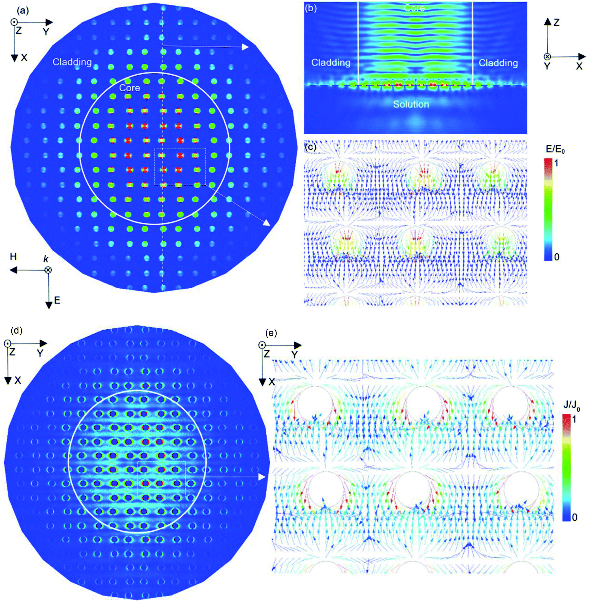 | ||
| Fig. 3 E-field distribution at the resonance wavelength 1.28 μm for four-hole group with 1 mg ml−1 concentration: (a) in XY plane and (b) in XZ plane. (c) The E-field vector. Current distribution at the resonate wavelength 1.28 μm for four-hole group with 1 mg ml−1 concentration: (d) current normalized magnitude and (e) current vector. | ||
 | ||
| Fig. 4 Reflected spectrum of fiber: (a) three-holes group on fiber tip, (b) four-holes group on fiber tip, (c) wavelength shift versus concentrations for (a) and (d) wavelength shift versus concentrations for (b). The simulated sensitivity for three-holes group is 890 nm per RIU and 660 nm per RIU for four-holes group. | ||
Results and discussion
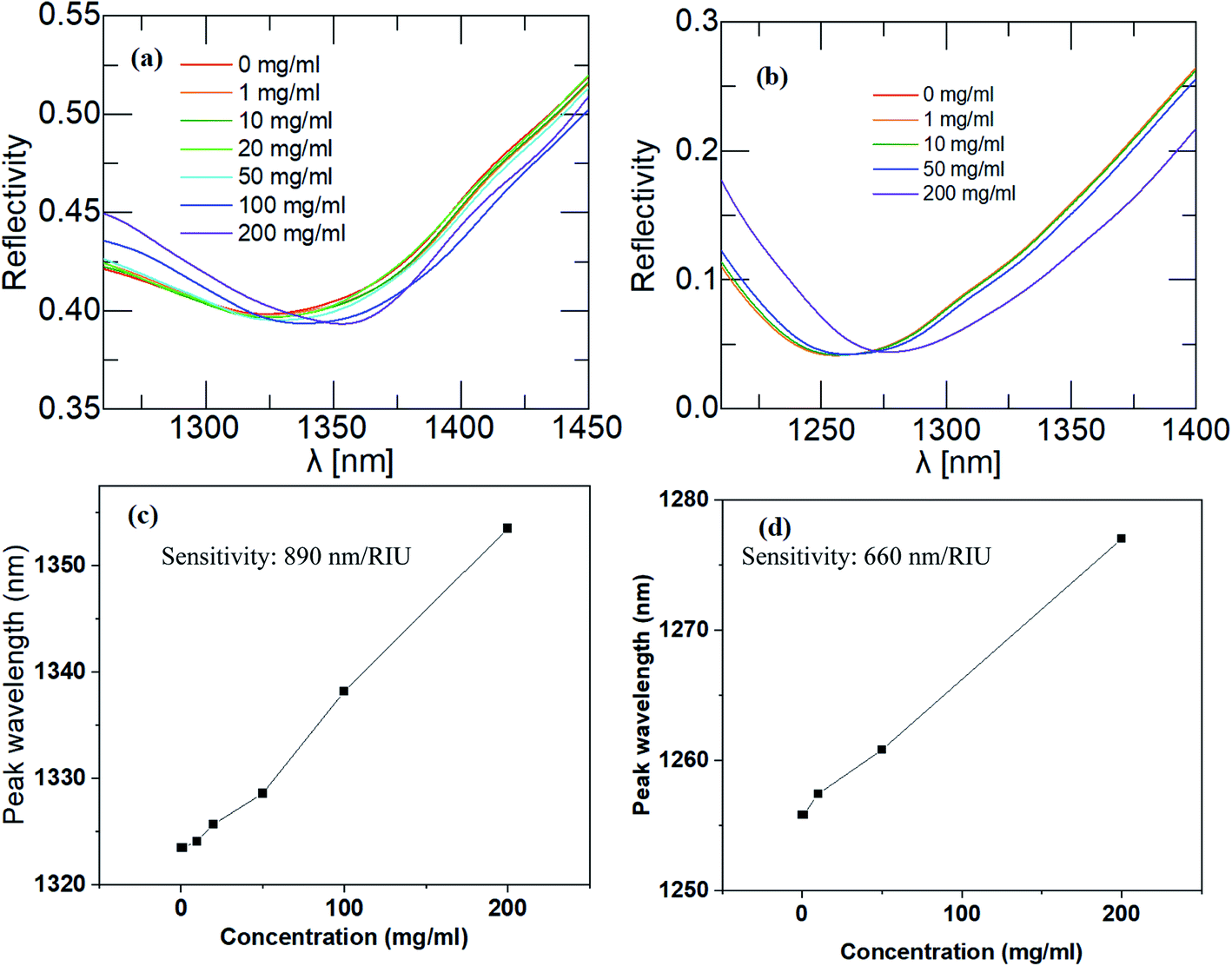
The experimental setup for reflection-based configuration used to test the device ability to differentiate among various mediums is shown in Fig. 5. A wide band light source, made of 4 light emitting diodes (LEDs), and an optical signal analyzer (OSA) with the resolution of 0.5 nm was connected to two ends of a standard 2 × 1 single mode optical fiber coupler (50%/50% split). The sensing single mode fiber (SMF) was fused to the other end of the fiber coupler. The light source feeds a 400 nm light spectrum to sensing fiber via the optical fiber coupler, where it interacts with the Al hole array at the fiber tip, modified and reflected it back, and detected by the OSA. We have studied the effect of changing the refractive index (RI) using water and various concentrations of sugar in water. The location of the dip of the reflected light spectrum depends on the hole diameter in Al layer, periodicity, and thickness of Al layer to validate our simulation model as well as demonstrate the feasibility of MPL fabrication technique on RI sensor, we measured the reflection spectra for pure water (concentration = 0), and glucose solution with concentration of 0.5–200 mg ml−1, respectively. Fig. 6a shows the reflected light spectra of water and various concentration of glucose for three-hole group array with diameters of 400 nm. Fig. 6b shows the reflected light spectra of water and various concentration of glucose for four-holes group array with diameters of 390 nm. Fig. 6c and d shows the linear fit for wavelength shift versus concentrations for (c) fiber that has three-holes group, the measured sensitivity was 906 nm per RIU, and (d) fiber that has four-holes group on fiber tip, the sensitivity was found to be 675 nm per RIU. It is noted that the sensitivity for 3 holes is better than that of 4 holes. We can see that from both the simulations and the experimental results. But this is only for the narrow wavelength range from 1250 nm to 1500 nm which is limited by our optical signal analyzer capability. It is also noted that as the number of holes increases, the peak shifts to the left and then disappear. Therefore, we believe that the 4 holes and 5 holes fiber sensor may have a better sensitivity in the outside the range that we can currently measure. We are testing both 3 holes and 4 holes in order to demonstrate the sensor with different patterns have the capability to sense glucose concentration change. And each of the pattern we created in the paper has the potential to be utilized for different purpose based on the applications, which we will try to investigate in the future work. The bandwidth of the reflected spectrum is part of the sensing performance. Commonly, when the reflected spectrum has a narrower bandwidth or when the resonance spectrum/dip is sharp, the sensor is more sensitive and thus has a better sensing performance. We will enhance the fiber sensor sensitivity by optimizing the aluminum disk pattern thickness, periodicity,44 and diameter to achieve much narrower bandwidth and hence improve the sensitivity. We will also investigate into the polarization and temperature dependence in the future publication.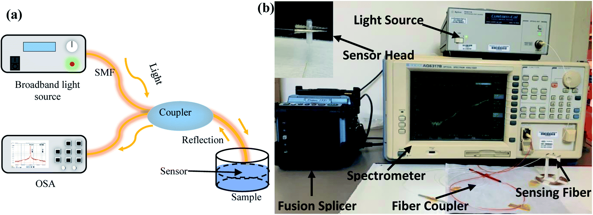 | ||
| Fig. 5 (a) Experimental testing setup of the RI sensor. The setup has a light source, bifurcated single-mode fiber cable, our sensor, and a light spectrum analyzer. (b) Characterizing system: sensing fiber fixed on a 3D printed rack is connected to the spectrometer and light source through a fiber coupler. The spectrometer will record the signal reflected from the sensing fiber tip. A fusion splicer is for splicing the sensing fiber to the fiber coupler, inserted is the magnified view of the sensing fiber. | ||
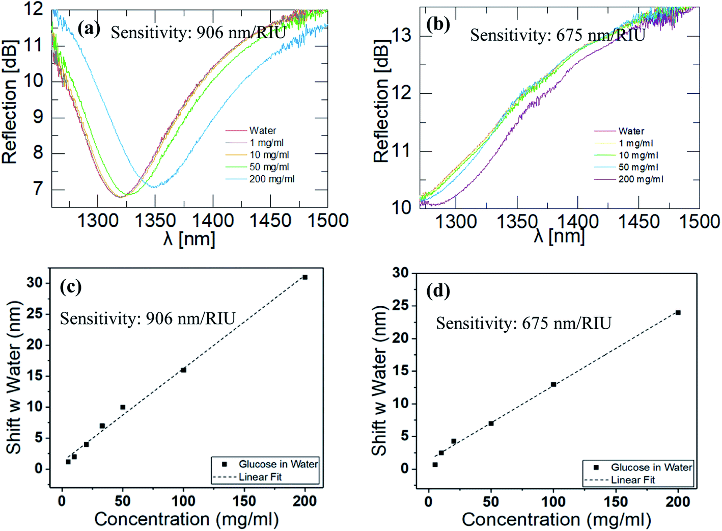 | ||
| Fig. 6 Experimental results of the RI sensor with the fiber tip patterned with three-holes group and tested in glucose (a) with a measured sensitivity of 906 nm per RIU, four-holes group and tested in glucose (b) with a measured sensitivity of 675 nm per RIU. Linear fit was plotted for wavelength shift versus concentrations for (c) fiber that has three-holes group, the measured sensitivity was 906 nm per RIU, and (d) fiber that has four-holes group on fiber tip, the sensitivity was found to be 675 nm per RIU. | ||
Conclusions
A reflection mode fiber optic based on extraordinary optical transmission (EOT) for the identification of the refractive index was designed fabricated and tested. The EOT structure was fabricated using microspheres photolithography to create a metasurface on the tip of a standard single mode fiber optic. By adjusting the array period and hole size, the EOT spectrum could be tuned to operate near the IR wavelength range, where high power optical sources are available for sensor interrogation and instrumentation. The fabricated EOT fiber probes have been demonstrated for in situ monitoring of ambient refractive index changes using DI-water and glucose solutions. The simulation results agree well with these measurement results. By creating nano holes in polysilicon layer on the fiber tip, the EOT sensor was successfully evaluated for glucose sensing. The wavelength shifts of the EOT spectrum showed a linear response to the ambient refractive index change.Author contributions
J. L. and I. J, conducted the fabrication, testing and data analysis. T. L. conducted the simulation. J. H. provided with equipment at the beginning. M. A. and E. K. conceived the experiments and design.Conflicts of interest
The authors declare no conflicts of interests.Acknowledgements
This project is supported in part by Applied Optoelectronics Incorporated (AOI), and NSF CMMI 1653792.References
- X.-D. Wang and O. S. Wolfbeis, Fiber-Optic Chemical Sensors and Biosensors, Anal. Chem., 2013, 85(2), 487–508, DOI:10.1021/ac303159b.
- H. P. Ho, W. C. Law, S. Y. Wu, X. H. Liu, S. P. Wong, C. Lin and S. K. Kong, Phase-Sensitive Surface Plasmon Resonance Biosensor Using the Photoelastic Modulation Technique, Sens. Actuators, B, 2006, 114(1), 80–84, DOI:10.1016/j.snb.2005.04.007.
- M. Sanders, Y. Lin, J. Wei, T. Bono and R. G. Lindquist, An Enhanced LSPR Fiber-Optic Nanoprobe for Ultrasensitive Detection of Protein Biomarkers, Biosens. Bioelectron., 2014, 61, 95–101, DOI:10.1016/j.bios.2014.05.009.
- S. Enoch and N. Bonod, Plasmonics: From Basics to Advanced Topic, accessed Mar 26, 2020, http://link.springer.com/10.1007/978-3-642-28079-5. DOI: DOI:10.1007/978-3-642-28079-5.
- E. J. Smythe, M. D. Dickey, B. Jiming, G. M. Whitesides and F. Capasso, Optical Antenna Arrays on a Fiber Facet for in Situ Surface-Enhanced Raman Scattering Detection, Nano Lett., 2009, 9(3), 1132–1138, DOI:10.1021/nl803668u.
- Y. Liang, Z. Yu, L. Li and T. Xu, A Self-Assembled Plasmonic Optical Fiber Nanoprobe for Label-Free Biosensing, Sci. Rep., 2019, 9(1), 1–7, DOI:10.1038/s41598-019-43781-8.
- J. Jatschka, A. Dathe, A. Csáki, W. Fritzsche and O. Stranik, Propagating and Localized Surface Plasmon Resonance Sensing - A Critical Comparison Based on Measurements and Theory, Sens. Bio-Sens. Res., 2016, 7, 62–70, DOI:10.1016/j.sbsr.2016.01.003.
- A. Iadicicco, S. Campopiano, A. Cutolo, M. Giordano and A. Cusano, Refractive Index Sensor Based on Microstructured Fiber Bragg Grating, IEEE Photonics Technol. Lett., 2005, 17(6), 1250–1252, DOI:10.1109/lpt.2005.846570.
- J. Wo, G. Wang, Y. Cui, Q. Sun, R. Liang, P. P. Shum and D. Liu, Refractive Index Sensor Using Microfiber-Based Mach–Zehnder Interferometer, Opt. Lett., 2012, 37(1), 67, DOI:10.1364/ol.37.000067.
- D. K. C. Wu, B. T. Kuhlmey and B. J. Eggleton, Ultra-Sensitive Photonic Crystal Fiber Refractive Index Sensor. in Optics InfoBase Conference Papers; Optical Society of America, 2009. 34, pp. 322–324. DOI: DOI:10.1364/ol.34.000322.
- V. Duong Ta, R. Chen, L. Ma, Y. Jun Ying and H. Dong Sun, Whispering Gallery Mode Microlasers and Refractive Index Sensing Based on Single Polymer Fiber, Laser Photon. Rev., 2013, 7(1), 133–139, DOI:10.1002/lpor.201200074.
- M. Mesch, C. Zhang, P. V. Braun and H. Giessen, Functionalized Hydrogel on Plasmonic Nanoantennas for Noninvasive Glucose Sensing, ACS Photonics, 2015, 2(4), 475–480, DOI:10.1021/acsphotonics.5b00004.
- B. Culshaw, Optical Fiber Sensor Technologies: Opportunities and-Perhaps-Pitfalls, J. Lightwave Technol., 2004, 22(1), 39–50, DOI:10.1109/JLT.2003.822139.
- J. M. Tam, L. Song and D. R. Walt, DNA Detection on Ultrahigh-Density Optical Fiber-Based Nanoarrays, Biosens. Bioelectron., 2009, 24(8), 2488–2493, DOI:10.1016/j.bios.2008.12.034.
- M. J. Aernecke and D. R. Walt, Optical-Fiber Arrays for Vapor Sensing, Sens. Actuators, B, 2009, 142(2), 464–469, DOI:10.1016/j.snb.2009.06.054.
- A. M. Shrivastav, S. K. Mishra and B. D. Gupta, Fiber Optic SPR Sensor for the Detection of Melamine Using Molecular Imprinting, Sens. Actuators, B, 2015, 212, 404–410, DOI:10.1016/j.snb.2015.02.028.
- P. Bhatia and B. D. Gupta, Surface-Plasmon-Resonance-Based Fiber-Optic Refractive Index Sensor: Sensitivity Enhancement, Appl. Opt., 2011, 50(14), 2032–2036, DOI:10.1364/ao.50.002032.
- N. Liu, L. Shi, S. Zhu, X. Xu, S. Yuan and X. Zhang, Whispering gallery modes in a single silica microparticle attached to an optical microfiber and their application for highly sensitive displacement sensing, Opt. Express, 2018, 26, 195–203 CrossRef CAS PubMed.
- H. Zhou, R. Ma, S. Zhu, H. Chen, G. Zhang, L. Shi and X. Zhang, Tunable polarization beam splitter and broadband optical power sensor using hybrid microsphere resonators, Opt. Express, 2020, 28, 32847–32857 CrossRef CAS PubMed.
- P. Jia and J. Yang, Integration of Large-Area Metallic Nanohole Arrays with Multimode Optical Fibers for Surface Plasmon Resonance Sensing, Appl. Phys. Lett., 2013, 102(24), 243107, DOI:10.1063/1.4811700.
- X. He, H. Yi, J. Long, X. Zhou, J. Yang and T. Yang, Plasmonic Crystal Cavity on Single-Mode Optical Fiber End Facet for Label-Free Biosensing, Appl. Phys. Lett., 2016, 108(23), 231105, DOI:10.1063/1.4953413.
- X. Lan, B. Cheng, Q. Yang, J. Huang, H. Wang, Y. Ma, H. Shi and H. Xiao, Reflection Based Extraordinary Optical Transmission Fiber Optic Probe for Refractive Index Sensing, Sensors Actuators, B, 2014, 193, 95–99, DOI:10.1016/j.snb.2013.11.046.
- A. Dhawan, J. F. Muth, D. N. Leonard, M. D. Gerhold, J. Gleeson, T. Vo-Dinh and P. E. Russell, Focused in Beam Fabrication of Metallic Nanostructures on End Faces of Optical Fibers for Chemical Sensing Applications, J. Vac. Sci. Technol., B: Microelectron. Nanometer Struct., 2008, 26(6), 2168–2173, DOI:10.1116/1.3013329.
- Y. Lin, Y. Zou, Y. Mo, J. Guo and R. G. Lindquist, E-Beam Patterned Gold Nanodot Arrays on Optical Fiber Tips for Localized Surface Plasmon Resonance Biochemical Sensing, Sensors, 2010, 10(10), 9397–9406, DOI:10.3390/s101009397.
- Y. Lin, Y. Zou and R. G. Lindquist, A Reflection-Based Localized Surface Plasmon Resonance Fiber-Optic Probe for Biochemical Sensing, Biomed. Opt. Express, 2011, 2(3), 478, DOI:10.1364/boe.2.000478.
- M. Consales, A. Ricciardi, A. Crescitelli, E. Esposito, A. Cutolo and A. Cusano, Lab-on-Fiber Technology: Toward Multifunctional Optical Nanoprobes, ACS Nano, 2012, 6(4), 3163–3170, DOI:10.1021/nn204953e.
- S. Feng, S. Darmawi, T. Henning, P. J. Klar and X. Zhang, A Miniaturized Sensor Consisting of Concentric Metallic Nanorings on the End Facet of an Optical Fiber, Small, 2012, 8(12), 1937–1944, DOI:10.1002/smll.201102290.
- H. Nguyen, F. Sidiroglou, S. F. Collins, T. J. Davis, A. Roberts and G. W. Baxter, A Localized Surface Plasmon Resonance-Based Optical Fiber Sensor with Sub-Wavelength Apertures, Appl. Phys. Lett., 2013, 103(19), 193116, DOI:10.1063/1.4829530.
- J. Cao, E. K. Galbraith, T. Sun and K. T. V. Grattan, Cross-Comparison of Surface Plasmon Resonance-Based Optical Fiber Sensors with Different Coating Structures, IEEE Sens. J., 2012, 12(7), 2355–2361, DOI:10.1109/jsen.2012.2188713.
- S. Shi, L. Wang, R. Su, B. Liu, R. Huang, W. Qi and Z. He, A Polydopamine-Modified Optical Fiber SPR Biosensor Using Electroless-Plated Gold Films for Immunoassays, Biosens. Bioelectron., 2015, 74, 454–460, DOI:10.1016/j.bios.2015.06.080.
- P. Malara, A. Crescitelli, V. Di Meo, A. Giorgini, S. Avino, E. Esposito, A. Ricciardi, A. Cusano, I. Rendina, P. De Natale and G. Gagliardi, Resonant Enhancement of Plasmonic Nanostructured Fiber Optic Sensors, Sens. Actuators, B, 2018, 273, 1587–1592, DOI:10.1016/j.snb.2018.07.030.
- X. Lan, B. Cheng, Q. Yang, J. Huang, H. Wang, Y. Ma, H. Shi and H. Xiao, Reflection Based Extraordinary Optical Transmission Fiber Optic Probe for Refractive Index Sensing, Sens. Actuators, B, 2014, 193, 95–99, DOI:10.1016/j.snb.2013.11.046.
- P. Jia, Z. Yang, J. Yang and H. Ebendorff-Heidepriem, Quasiperiodic Nanohole Arrays on Optical Fibers as Plasmonic Sensors: Fabrication and Sensitivity Determination, ACS Sens., 2016, 1(8), 1078–1083, DOI:10.1021/acssensors.6b00436.
- J. Liu, I. Jasim, C. Zhu, M. Roman, E. Kinzel, J. Huang and M. Almasri, Microsphere Photolithography Patterning of Plasmonic Sensors on Optical Fiber, IEEE Research and Applications of Photonics in Defense Conference (RAPID), 2019, pp. 1–2, DOI: DOI:10.1109/rapid.2019.8864312.
- M. Pisco, F. Galeotti, G. Quero, G. Grisci, A. Micco, L. V. Mercaldo, P. D. Veneri, A. Cutolo and A. Cusano, Nanosphere Lithography for Optical Fiber Tip Nanoprobes, Light Sci. Appl., 2017, 6(5), e16229, DOI:10.1038/lsa.2016.229.
- J. Liu, I. Jasim, C. Zhu, M. Roman, Y. Yang, C. Qu, J. Huang, E. Kinzel and M. Almasri, Functional Plasmonic Fiber-Optic Based Sensors Using Low-Cost Microsphere Photolithography, International Conference on Solid-State Sensors, Actuators and Microsystems & Eurosensors XXXIII (TRANSDUCERS & EUROSENSORS XXXIII), 2019, pp. 1545–1548, DOI: DOI:10.1109/transducers.2019.8808390.
- I. Antohe, D. Spasic, F. Delport, J. Li and J. Lammertyn, Nanoscale Patterning of Gold-Coated Optical Fibers for Improved Plasmonic Sensing, Nanotechnology, 2017, 28(21), 215301, DOI:10.1088/1361-6528/aa6b53.
- Y. Zhang, T. Wei, Z. Xiong, L. Shang, Y. Tian, Y. Zhao, P. Zhou, J. Wang and J. Li, Enhanced Optical Power of GaN-Based Light-Emitting Diode with Compound Photonic Crystals by Multiple-Exposure Nanosphere-Lens Lithography, Appl. Phys. Lett., 2014, 105(1), 13108, DOI:10.1063/1.4889745.
- A. Bonakdar, S. J. Jang and H. Mohseni, Novel High-Throughput and Maskless Photolithography to Fabricate Plasmonic Molecules, J. Vac. Sci. Technol., B: Nanotechnol. Microelectron.: Mater., Process., Meas., Phenom., 2014, 32(2), 20604, DOI:10.1116/1.4865999.
- C. Qu and E. C. Kinzel Thermal Radiation from Microsphere Photolithography Patterned Metasurfaces. In ASME 2017 Heat Transfer Summer Conference, HT 2017, American Society of Mechanical Engineers, 2017. 2. DOI: DOI:10.1115/ht2017-5098.
- A. Bonakdar, M. Rezaei, E. Dexheimer and H. Mohseni, High-Throughput Realization of an Infrared Selective Absorber/emitter by DUV Microsphere Projection Lithography, Nanotechnology, 2016, 27(3), 35301, DOI:10.1088/0957-4484/27/3/035301.
- W. Guo, Z. B. Wang, L. Li, D. J. Whitehead, B. S. Luk'yanchuk and Z. Liu, Near-Field Laser Parallel Nanofabrication of Arbitrary-Shaped Patterns, Appl. Phys. Lett., 2007, 90(24), 243101, DOI:10.1063/1.2748035.
- K. M. McPeak, S. V. Jayanti, S. J. P. Kress, S. Meyer, S. Iotti, A. Rossinelli and D. J. Norris, Plasmonic films can easily be better: rules and recipes, ACS photonics, 2015, 2(3), 326–333, DOI:10.1021/ph5004237.
- I. Jasim. J. Liu, C. Zhu, M. Roman, J. Huang, E. Kinzel and M. Almasri, Microsphere Photolithography Patterned Nanohole Array on an Optical Fiber, in IEEE Access, 2021. 9, pp. 32627–32633, DOI: DOI:10.1109/access.2021.3059439.
Footnote |
| † The first two authors have equal contributions this project and paper. |
| This journal is © The Royal Society of Chemistry 2021 |