DOI:
10.1039/D1RA02578C
(Paper)
RSC Adv., 2021,
11, 17538-17546
Transparent and flexible ZnO nanorods induced by thermal dissipation annealing without polymer substrate deformation for next-generation wearable devices†
Received
1st April 2021
, Accepted 7th May 2021
First published on 13th May 2021
Abstract
The fabrication of a transparent and flexible ultraviolet photodetector based on hydrothermally grown ZnO nanorods requires an annealing step to render the sol–gel spin-coated ZnO seed layer crystalline. As high-temperature annealing deforms low-melting-point polymer substrates, we herein devised a thermal dissipation annealing (TDA) method in which heat transfer to ZnO thin films is synchronized with heat release from the polymer substrate to crystallize the ZnO seed layer without polymer substrate deformation and melting. ZnO nanorods (NRs) were hydrothermally grown on non-annealed and annealed ZnO seed layers, and NR density and diameter were shown to be higher in the latter case, as the crystallized ZnO seed layer provided heterogeneous nucleation sites for NR growth. In addition, the larger density and diameter of ZnO NRs grown on the annealed ZnO seed layer were confirmed by analysis of O 1s signal intensities. A transparent and flexible UV photodetector based on ZnO NRs grown on the annealed ZnO seed layer exhibited a higher photocurrent/dark current ratio, photosensitivity, and photoresponsivity than that fabricated using a non-annealed seed layer. Taken together, the above results suggest that the TDA method is an effective way of fabricating transparent and flexible UV photodetectors with high photosensitivity, photoresponsivity, and photocurrent stability and it means that the next generation wearable devices can be easily realized by using the TDA method.
1. Introduction
Transparent and flexible optoelectronics offering the benefits of stability, flexibility, and low weight are the key components of next-generation devices such as transparent displays, energy storage systems, UV photodetectors, gas sensors, solar cells, and wearables.1–5 In particular, UV photodetectors attract much interest due to their great application potential in diverse fields such as secure space-to-space communication, pollution monitoring, water sterilization, flame sensing, and missile plume detection.6–9 However, to be practically applicable, these photodetectors should exhibit high optical transparency, flexibility, chemical stability, good mechanical properties, and biocompatibility. Among the various semiconductors, ZnO, a II–VI compound semiconductor with a wurtzite structure, is well suited for the fabrication of transparent and flexible UV photodetectors, offering the benefits of a wide direct bandgap (3.37 eV), large exciton binding energy (60 meV), high thermal stability, non-toxicity, and biocompatibility.10–14 Moreover, ZnO exhibits the additional advantages of high electron mobility and high transparency in the visible region and it makes the ZnO to be applied in a various fields.15–18 Compared to the common Si-based UV photodetectors, which require (i) complex filters to avoid noise due to the low electron energies and the narrow bandgap of Si and (ii) ultrahigh vacuum and high voltages for accurate detection, ZnO-based detectors can be used without filters for the reasons described above.19,20 In addition, one-dimensional (1D) ZnO nanostructures such as nanorods (NRs), nanobelts, nanotubes, nanotips, and nanofibers exhibit quantum mechanical confinement effects and high surface-to-volume ratios and are therefore often used for the fabrication of high-performance UV photodetectors.21–23 Over the past few decades, much effort has been directed at the fabrication of transparent and flexible UV photodetectors based on heterojunctions with compound semiconductors.24–26 However, these techniques are time-consuming and costly, as the manufacturing process is complicated and affords low-crystallinity ZnO, which is poorly suited for high-performance transparent and flexible UV photodetectors. In addition, the above methods of fabricating UV photodetectors satisfying both flexibility and transparency requirements still face many challenges. Conversely, hydrothermal methods allow the easy growth of ZnO NRs and offer the advantages of operation simplicity, no need for complicated equipment, broad substrate scope, low cost, environmental friendliness, and large growth area.27–29 Especially, low growth temperatures (<120 °C) are beneficial for the fabrication of transparent and flexible UV photodetectors, as polymer substrates such as polyethylene naphthalate (PEN), polyethylene terephthalate, polyimide, and mica easily deform at >200 °C because of their low melting points and glass transition temperatures. Also, the morphology of hydrothermally grown ZnO NRs can be easily controlled by the choice of seed layer type, pH, growth temperature, and precursor solution rotation.30–33 Despite their advantages, fabrication of transparent and flexible UV photodetectors by using hydrothermal method face an important drawback, the process of ZnO seed layer annealing. In hydrothermal methods, the ZnO seed layer plays a crucial role in ZnO NR growth for the following reasons. First, when ZnO NRs are hydrothermally grown on the ZnO seed layer, this layer acts as a homoepitaxy, and the energy of the substrate–ZnO nuclei interface (and hence, the nucleation barrier) decreases. Second, the abundant interfaces between seeds, which have high energy, make the ZnO nuclei easily adhere to the seed layer surface. In previous studies dealing with the hydrothermal growth of ZnO NRs on the ZnO seed layer, seed layer was commonly deposited by sol–gel spin-coating techniques, which offer the advantages of high deposition rate, low cost, simplicity, large deposition area, and ease of dopant incorporation.34–36 However, when the ZnO seed layer is deposited onto a polymer substrate for the hydrothermal growth of ZnO NRs, the low crystallinity and abundant defect sites of sol–gel spin-coated ZnO thin films result in free electron trapping and therefore deteriorate the performance of ZnO-based UV photodetectors.37 Therefore, to fabricate high-performance transparent and flexible UV photodetectors using hydrothermally grown ZnO NRs, the amorphous ZnO seed layer has to be made crystalline. Based on the recent studies on the crystallization of amorphous ZnO thin films, various annealing methods have been devised, with the most common one featuring the crystallization of ZnO thin films by thermal annealing in a furnace.38–40 Farooqi et al. applied this method to sol–gel spin-coated ZnO thin films and probed the effects of annealing temperature.41 However, the high temperatures used for thermal annealing (>500 °C) cause the deformation and melting of polymer substrates and promote the generation of lattice misfits due to the differences in the thermal expansion coefficient of ZnO thin films and substrates, thus resulting in low photocurrents. As an alternative, laser annealing methods can be used to crystallize amorphous ZnO thin films; however, the laser annealing of sol–gel spin-coated ZnO thin films decreases their transparency, as the increase in grain boundary density enhances photon scattering.42,43 In addition, before laser annealing, the amorphous ZnO thin films have to be subjected to rapid thermal annealing to ensure complete crystallization. This additional annealing process increases the number of oxygen vacancies and thus deteriorates the performance of ZnO-based optoelectronics. Additionally, electron beam and excimer laser annealing processes are unsuitable, as the high energy densities of excimer lasers and electron beams result in polymer substrate deformation.44,45 To anneal sol–gel derived ZnO thin films without bending polymer substrates, we previously devised a novel annealing method, termed counterpoise-assisted annealing (CAA), in which an external force is applied by placing a counterpoise on ZnO thin films.46 Although the CAA method is compatible with transparent and flexible polymer substrates, the substrate scope is limited to muscovite mica and high-melting point (400 °C) polyimide. Therefore, to hydrothermally fabricate transparent and flexible UV photodetectors based on polymer substrates, one should develop a new method of annealing sol–gel spin-coated ZnO thin films without substrate melting or deformation. Herein, we recently developed a novel method named thermal dissipation annealing (TDA) method, in which the substrate thermal energy is eliminated through a thermal dissipation annealing system integrated with an IR lamp and a cold plate to prevent the melting of polymer substrates.47,48 In other words, when a ZnO thin film is annealed by the TDA method, the substrate with ZnO thin film is placed on a cold plate held at −10 °C, and the IR lamp is activated to induce annealing. As a result, a temperature difference is generated between the surface and the bottom of the ZnO thin film and gradually increases with progressing annealing. This temperature difference is related to the mobility difference of ZnO at the surface and bottom of the thin film. As a result, TDA-based annealing reduces the number of defects and transforms amorphous ZnO thin films into single-crystalline ones. Hence, ZnO seed layers annealed by the TDA method allow the growth of highly crystalline ZnO NRs and thus promote the fabrication of high-performance optoelectronics for diverse applications.
In this study, we deposited a ZnO seed layer on PEN using a sol–gel spin-coating method and subjected this layer to TDA method. In addition, ZnO NRs were hydrothermally grown on non-annealed and annealed (TDA-processed) ZnO seed layers for comparison. Further, we fabricated a transparent and flexible ZnO-based UV photodetector to demonstrate the suitability of the TDA method for the fabrication of next-generation wearable optoelectronics devices.
2. Experiment
2.1 Preparation of ZnO seed layer
To deposit the ZnO seed layer by using sol–gel spin-coating method, ZnO sol–gel solution was prepared by dissolving zinc acetate dihydrate ([Zn(CH3COO)2·2H2O], guaranteed reagent, ≥99.0%, JUNSEI) and monoethanolamine (MEA) ([NH2CH2CH2OH], ACS reagent, ≥99.0%, Sigma-Aldrich) in 2-methoxyethanol ([C3H8O2], guaranteed reagent, ≥99.0%, JUNSEI) and the MEA was used to stabilize the solution and enhance the solubility of the precursor salt. The zinc acetate/MEA molar ratio equalled 1![[thin space (1/6-em)]](https://www.rsc.org/images/entities/char_2009.gif) :1, and the concentration of the ZnO precursor solution was 0.5 M. The prepared mixture was stirred at 60 °C for 2 h to obtain a clear homogeneous solution that was used as a coating source after being cooled to room temperature. For PEN substrate, the cleaning is progressed by immersing PEN substrates in isopropyl alcohol for 20 min with ultrasonication, and rinsed with DI water for 2 min, and dried with N2 gas (99.9999%). The sol–gel solution spin-coated onto the cleaned PEN substrate at 2000 rpm for 20 s and the spin-coated ZnO seed layers were preheated at 150 °C for 10 min in an oven. The spin-coating and preheating processes was repeated four times. Subsequently, the obtained ZnO thin films were annealed at 500 °C for 1 h by using the TDA method.
:1, and the concentration of the ZnO precursor solution was 0.5 M. The prepared mixture was stirred at 60 °C for 2 h to obtain a clear homogeneous solution that was used as a coating source after being cooled to room temperature. For PEN substrate, the cleaning is progressed by immersing PEN substrates in isopropyl alcohol for 20 min with ultrasonication, and rinsed with DI water for 2 min, and dried with N2 gas (99.9999%). The sol–gel solution spin-coated onto the cleaned PEN substrate at 2000 rpm for 20 s and the spin-coated ZnO seed layers were preheated at 150 °C for 10 min in an oven. The spin-coating and preheating processes was repeated four times. Subsequently, the obtained ZnO thin films were annealed at 500 °C for 1 h by using the TDA method.
2.2 Growth of ZnO NRs
For the growth of ZnO NRs on three type of ZnO seed layer, the precursor solution was prepared by mixing zinc nitrate hexahydrate ([Zn(NO3)2·6H2O], guaranteed reagent, ≥98.0%, Sigma-Aldrich) and hexamethylenetetramine (HMT) ([(CH2)6N4], ACS reagent, ≥98.0%, Sigma-Aldrich) and the concentration of precursor solution was 0.025 M. The PEN substrates with two type of ZnO seed layer was fixed in Teflon-lined autoclave which filled up with prepared precursor solution, and the growth of ZnO NRs through hydrothermal method was proceeded at 140 °C for 4 h. After the completion of the growth, the hydrothermally grown ZnO nanorods were rinsed with DI water and dried with high-purity N2 gas. To avoid confusion, a schematic for each type of ZnO NRs with growth and annealing conditions is shown in Fig. S1.†
2.3 Characterization
The morphology of the ZnO thin films was measured by field-emission scanning electron microscopy (FE-SEM) (TESCAN MIRA3) on an instrument with an accelerating voltage of 30 kV. The crystal phases were analysed by X-ray diffraction (XRD) (PANalytical X'Pert Pro) using a Cu-Kα radiation source (λ = 0.15406 nm) at an accelerating voltage of 40 kV. The surface chemical analysis was investigated by X-ray photoelectron spectroscopy (XPS) (Thermo VG Scientific, K-alpha) with 300 W Al Kα radiation. The optical properties were analysed by using photoluminescence (PL) spectroscopy (Horiba, Triax 550) performed using a He–Cd laser with an excitation power of 20 mW and equipped with a 0.75 m single-grating monochromator with a photomultiplier tube. In addition, the UV photoresponse properties were measured at a bias voltage of 0.1 mV using a UV light (λ = 365 nm) with a power density of 0.375, 0.75, 1.125, and 1.5 W cm−2.
3. Results and discussion
Before describing the effect of TDA on the ZnO seed layer, one should comprehend the underlying mechanism of this treatment. During annealing process of TDA method, heat transfer to ZnO thin films can be synchronized with heat release from the substrate and amorphous ZnO thin films, and the crystallization of the sol–gel spin-coated ZnO seed layer proceeds through the synchronization of heating (IR lamp) and cooling (cold plate) processes. When ZnO thin films deposited on PEN were annealed using the IR lamp, the temperature of these films and the polymer substrate rapidly increased from 20 to 500 °C in just a few minutes, and hence, the temperature of ZnO thin films and the polymer substrate had to be decreased in advance to restrict polymer substrate deformation. Therefore, before annealing, the temperature of the cold plate was set to −10 °C, and the ZnO thin films deposited on the polymer substrate were placed on the cold plate for 30 s to prevent PEN deformation. As shown in Fig. 1(b) and (c), a sufficient amount of space was available between ZnO thin films and the quartz plate because of the presence of a mica plate with a hollow square at its center. This space was required to prevent the condensation of moisture. When ZnO thin films were subjected to TDA method without this separate space, moisture was formed, as the temperature of the ZnO thin film surface during 30 s cooling dropped to values below the dew point, which deteriorated the annealing efficiency and heat transfer rate. Moisture formation on the surface of ZnO thin films interrupted heat transfer to the same, and, as a result, the crystallization of these films was hindered. Therefore, the temperature decrease of ZnO thin films and PEN as well as the presence of a separate space were concluded to be essential for successful TDA method.
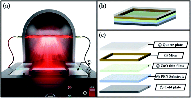 |
| | Fig. 1 Schematics images for annealing process of TDA method. | |
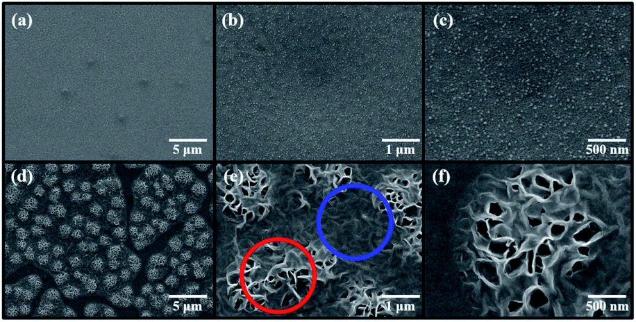
Fig. 2 shows the non-annealed and annealed (using TDA method) ZnO seed layers. In the former case, the surface featured ZnO particles, whereas in the latter case, 2D ZnO nanosheets were observed. In general, ZnO thin films deposited by sol–gel spin-coating exhibited a fibrous root structure comprising ZnO nanoparticles because of the slow cooling after pre-heating.49 However, when ZnO thin films were deposited on PEN substrate, pre-heating proceeded at temperatures lower than those used for ZnO thin films deposited on Si, glass, and quartz substrates because of the low melting point of PEN. Thus, the thermal energy and time were insufficient for ions to aggregate along the crystal planes having a similar lattice match to decrease their high surface energy, and the surface morphology of the non-annealed ZnO seed layer comprised ZnO nanoparticles as opposed to a fibrous root structure. In contrast, the TDA-processed ZnO seed layer featured 2D ZnO nanosheets with a fibrous structure. This morphological difference was related to the mobility difference of ZnO molecules at the surface and bottom of ZnO thin films.43,44 In other words, when the ZnO thin films were crystallized by TDA method, synchronized heating and cooling resulted in a temperature difference between the film surface and bottom. For TDA method, ZnO thin films were placed on a cold plate prior to annealing, which lowered the temperature of the film bottom. In addition, the surface temperature of ZnO thin films increased during annealing, whereas that of the film bottom stayed low. The ZnO molecules at the surface of ZnO thin films had an elevated mobility due to the large amount of thermal energy, whereas the ZnO at the films bottom had a decreased mobility due to the small amount of thermal energy and low temperature caused by heat dissipation. Therefore, ZnO molecules with high thermal energy moved to the bottom of the wrinkled network structures to reach thermal equilibrium, whereas ZnO molecules at the bottom of the wrinkled network structures rarely moved, which resulted in the formation of 2D ZnO nanosheets.
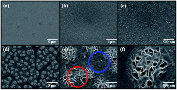 |
| | Fig. 2 FE-SEM images of (a–c) non-annealed ZnO seed layer and (d–f) ZnO seed layer annealed by using TDA method. | |
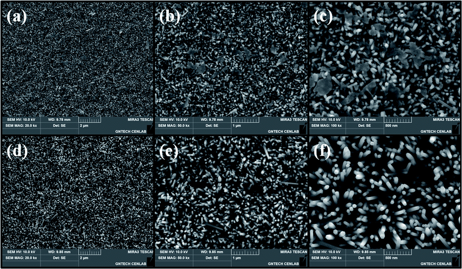
Fig. 3(a)–(c) show ZnO NRs (NR1s) grown on the non-annealed ZnO seed layer, while Fig. 4(d)–(f) show ZnO NRs (NR2s) grown on the TDA-processed ZnO seed layer. In the former case, the ZnO NRs and the ZnO plate were observed simultaneously, whereas only ZnO NR2s were observed when the annealed ZnO seed layer was immersed into the aqueous solution. In the case of the hydrothermal method, the crystalline ZnO seed layer is of high importance, as it provides heterogeneous nucleation sites for ZnO NR growth.50 At the initial stage of hydrothermal ZnO NR growth, Zn(OH)2 is formed in aqueous solution through the combination of Zn2+ and OH− ions and subsequently transforms into ZnO crystals (which act as nucleation sites) on the ZnO seed layer.51–53 When the concentration of ZnO reaches supersaturation, ZnO crystals grow in their typical habit to afford ZnO NRs. However, the amorphous ZnO seed layer is dissolved during the hydrothermal reaction to generate ZnO clusters in the aqueous solution. The size of these clusters gradually increases (because of the aggregation of small clusters and the combination of Zn2+ and OH− ions) to afford 2D ZnO nanosheets. Consequently, the formation of these nanosheets restricts the growth of ZnO NRs, and growth on the amorphous ZnO seed layer affords a smaller amount of ZnO NRs with decreased diameter and length, as shown in Fig. S2.† In addition, these results indicate that the crystallization possibility of the ZnO seed layer can be estimated by the observation of 2D ZnO nanosheets.
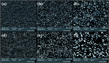 |
| | Fig. 3 FE-SEM images of (a–c) ZnO NR1s and (d–f) ZnO NR2s. | |
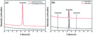 |
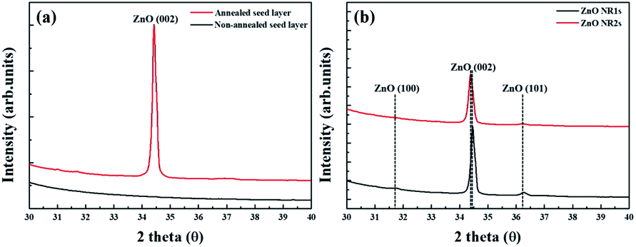
| | Fig. 4 XRD patterns of (a) ZnO seed layer and (b) ZnO NRs. | |
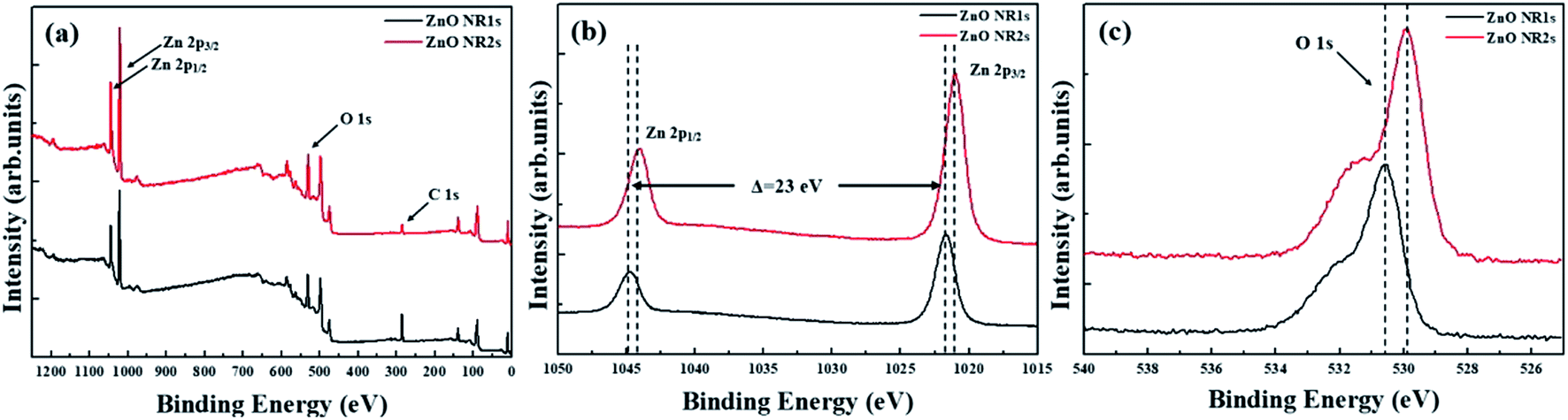
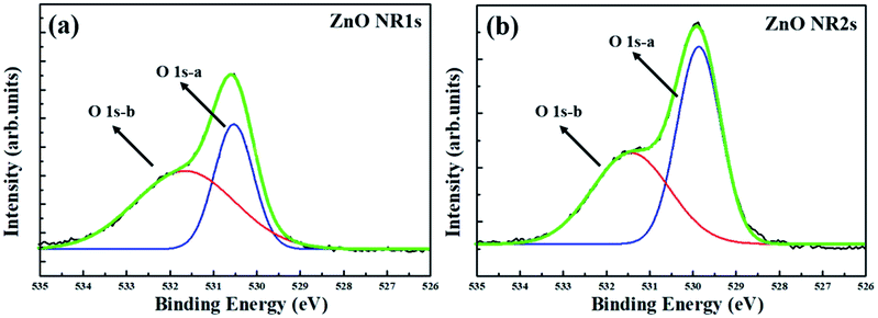
Fig. 4 shows the XRD patterns of non-annealed and annealed ZnO seed layers and the ZnO NRs grown on the two seed layer types. The pattern of the TDA-processed ZnO seed layer exhibited a strong diffraction at 34.4°, which was ascribed to the ZnO (002) plane, whereas the diffraction peak of ZnO could not be observed, which indicated that TDA method allows one to crystallize amorphous sol–gel spin-coated ZnO thin films.54 In the case of ZnO NRs, a strong ZnO (002) diffraction peak (34.6°) and two weak diffraction peaks of ZnO (100) and (101) planes (31.7 and 36.4°, respectively) were observed, indicating that ZnO NRs were grown with a c-axis orientation regardless of the crystallization of the ZnO seed layer. Furthermore, XPS was used to investigate the chemical composition of ZnO NRs grown on the ZnO seed layer. Fig. 5 shows typical survey spectra of ZnO NR1s and NR2s, revealing the presence of Zn and O. Regardless of growth conditions, the C 1s peak of carbon adsorbed on the surface of ZnO NRs during their exposure to the ambient atmosphere was observed at 284.08 eV. Fig. 6(b) presents raw high-resolution Zn 2p spectra, revealing the presence of two distinct peaks at 1044.81 eV (Zn 2p1/2) and 1044.12 eV (Zn 2p3/2).55,56 The splitting of the Zn 2p peaks (23 eV) indicated the occurrence of spin–orbit coupling.57 ZnO NR2s exhibited more intense Zn 2p peaks than ZnO NR1s. Moreover, the binding energies of these peaks were lower in the former case (1044.12 vs. 1044.81 eV and 1021.04 vs. 1021.72 eV). In general, the Zn 2p peaks were accurately assigned to ZnO, and their intensity increase was therefore due to the higher density and increased length/diameter of ZnO NRs. The shift of Zn 2p peak positions was related to a change in the chemical environment of surface atoms, specifically, to a change in the number of Zn atoms combined with O atoms. When the amorphous ZnO seed layer was processed by TDA, its crystallization increased the growth rate of ZnO NRs by providing heterogeneous nucleation sites. Thus, the amount of Zn–O bonds increased, and the Zn 2p peaks shifted to lower binding energies. The O 1s spectra of ZnO NR1s (grown on non-annealed ZnO seed layer) and ZnO NR2s (grown on TDA-processed ZnO seed layer) are shown in Fig. 5(c). The spectrum of ZnO NR1s showed a major peak at 530.63 eV with a small shoulder at 532.13 eV, while the spectrum of ZnO NR2s showed a major peak at 529.88 eV with a small shoulder at 531.53 eV. For an accurate comparison of oxygen chemical states, the O 1s spectra of ZnO NRs were fitted using Gaussian functions, with the results presented in Fig. 6(a) and (b). In the case of ZnO NR1s, the O 1s signal was deconvoluted into two components. The lower-binding-energy peak at 530.53 eV was attributed to O2− ions surrounded by Zn2+ ions in the wurtzite lattice, while the higher-binding-energy peak at 531.65 eV was attributed to chemisorbed or dissociated oxygen or OH species on the ZnO NRs surface.58,59 In the case of ZnO NR2s, the O 1s signal was deconvoluted into a stronger peak at 529.86 eV and a weaker peak at 531.43 eV. Interestingly, the intensity of the lower-binding-energy peak of ZnO NR2s exceeded that of ZnO NR1s, whereas the intensity of the higher-binding-energy peak was virtually independent of the type of the ZnO seed layer. This result suggests that because of their higher density and larger diameter, ZnO NR2s had higher amounts of O2− ions that were surrounded by Zn2+ ions in the wurtzite lattice. In addition, the O 1s binding energies of ZnO NR2s were shifted to lower values because of oxygen sufficiency was filled up and the electrons surrounding oxygen are reduced compared to the case of ZnO NR1s. The similar intensities of the higher-binding-energy O 1s component at ∼531 eV were due to the unchanged amount of interstitial oxygen generated in the ZnO lattice during hydrothermal growth.
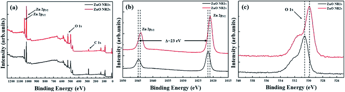 |
| | Fig. 5 (a) XPS Survey spectra for ZnO NRs, (b) XPS spectra of the Zn 2p core level regions, and (c) XPS spectra of the O 1s core level regions. | |
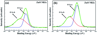 |
| | Fig. 6 Gaussian-fitted peaks for O 1 s of ZnO (a) NR1s and (b) NR2s. | |
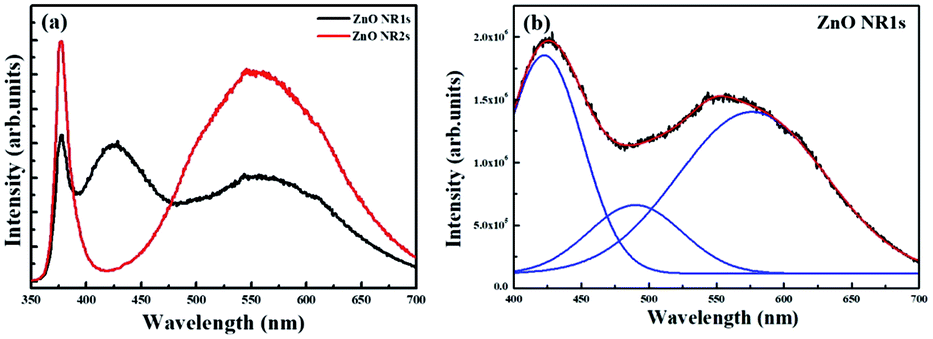
The optical properties of ZnO NRs grown on the two types of ZnO seed layers were probed by room-temperature PL spectroscopy. As shown in Fig. 7(a), the PL spectrum of ZnO NR2s featured a sharp peak ascribed to the near-band-edge (NBE) emission in the UV region and a broad peak ascribed to deep-level (DL) emission in the visible region, respectively.60,61 However, unlike the normal spectrum of ZnO NRs, the PL spectrum of ZnO NR1s featured a sharp emission in the UV region and two broad emissions in the visible region. In several studies, the NBE emission at 375 nm was attributed to exciton recombination, while DL emission was ascribed to defects such as oxygen vacancies, interstitial oxygen, zinc vacancies, antisite oxygen, and interstitial zinc.62–64 Herein, ZnO NR2s, which were grown on a TDA-processed ZnO seed layer, exhibited a two-fold higher NBE emission intensity than ZnO thin films grown on an amorphous ZnO seed layer. When TDA-processed ZnO thin films were used as the seed layer for the hydrothermal method, a greater amount of ZnO nuclei, which play a crucial role in the growth of ZnO NRs, were formed on the ZnO seed layer to increase the growth rate of ZnO NRs. In contrast, in the case of amorphous ZnO thin films, the density of ZnO nuclei formed on the seed layer was lower because of the dissolution of the amorphous ZnO seed layer during hydrothermal treatment, which resulted in a lower density of ZnO NRs. Thus, ZnO NR2s grown on the crystalline ZnO seed layer, on which ZnO nuclei can form, exhibited a more intense NBE emission than ZnO NRs grown on the non-annealed ZnO NRs because of the higher number of excitons in the former case. In the case of DL emission, the PL spectra of ZnO NR1s were fitted using Gaussian functions to enable an accurate comparison and determine the origin of DL emission. As shown in Fig. 7(b), three Gaussian peaks, attributed to interstitial zinc, antisite oxygen, and interstitial oxygen, were observed for ZnO NR1s at 425, 500, and 600 nm, respectively. The broad yellow emission observed at 550 nm for ZnO NR1s and NR2s was typical of ZnO NRs grown in an oxygen-rich environment. Herein, ZnO NRs were grown on two types of ZnO seed layers in aqueous solution, which caused the incorporation of interstitial and antisite oxygen into the ZnO lattice, in line with previous studies. In addition, the strongest fitted peak centered at 425 nm was ascribed to interstitial zinc. When the ZnO NRs were grown on amorphous ZnO thin films, the ZnO seed layer dissolved in the aqueous solution to form Zn2+ ions. During the growth process, the number of Zn2+ ions generated from zinc nitrate hexahydrate and the amorphous ZnO seed layer increased, and these ions entered ZnO NRs. As a result, ZnO NR1s grown in the aqueous solution with abundant Zn2+ and O2− ions contained interstitial oxygen and zinc.
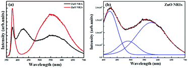 |
| | Fig. 7 (a) PL spectra of ZnO NR1s and NR2s and (b) Gaussian-fitted DL emission of ZnO NR1s. | |
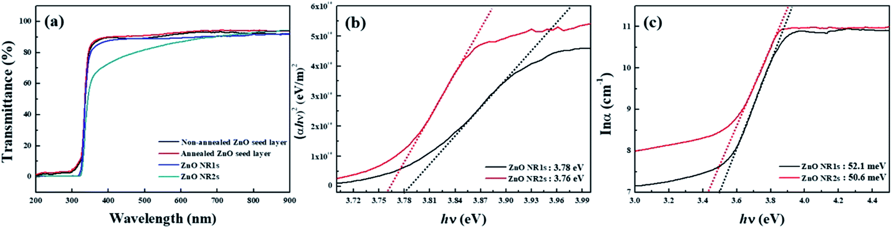
To confirm the possibility of fabricating transparent and flexible optoelectronics using the TDA method, we measured the transparency of the ZnO seed layer and ZnO NRs. As shown in Fig. 8(a), the TDA-processed ZnO seed layer exhibited a higher transmittance than the non-annealed ZnO seed layer, which was ascribed to the fact that the crystallization of ZnO thin films decreased light scattering. Considering hydrothermally grown ZnO NRs, ZnO NR1s exhibited an average transmittance of >80% in the visible region, whereas the transmittance of ZnO NR2s decreased from 90 to 70% as the wavelength decreased from 900 to 400 nm. Moreover, ZnO NR2s grown on the annealed ZnO seed layer exhibited a lower transmittance than ZnO NR1s because of the higher density of ZnO NRs in the latter case. The optical bandgaps of ZnO NR1s and NR2s were calculated from the corresponding Tauc plots using the following equation:
where
α is the absorption coefficient,
hν is the photon energy, and
Eg is the bandgap of ZnO NRs.
Fig. 8(b) shows a plot of (
αhν)
2 vs. hν.
65,66 The optical bandgap of ZnO NRs was estimated as the intercept with the energy axis obtained by extrapolating the straight-line part of the curve. The calculated optical bandgap of ZnO NR2s (3.76 eV) was lower than that of ZnO NR1s (3.78 eV), which was ascribed to the larger diameter of the former NRs. In other words, the conduction and valence band levels were red-shifted with increasing NR diameter, as quantum confinement effects resulted in a lower bandgap. The width of localized states available in the optical bandgap of ZnO NRs affected the optical bandgap structure, which is referred to as an Urbach tail and is related to a similar exponential tail. The absorption coefficient and photon energy near the band edge are related by the following equation:
| | |
α = α0exp(hν/EU)
| (2) |
where
α0 is a constant, and
EU is the Urbach energy corresponding to the width of the band tail.
67 Fig. 9(c) shows a plot of ln
α vs. hν used to determine the Urbach energy, which is related to the disorder of ZnO NR1s and NR2s. Specifically, Urbach energies were calculated from the reciprocal gradient of the linear portion of this graph as 52.1 meV (ZnO NR1s) and 50.3 meV (ZnO NR2s), indicating that the latter NRs featured lower structural disorder and improved crystallinity.
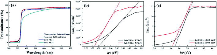 |
| | Fig. 8 (a) Transmittance spectra in the wavelength range from 200–900 nm, (b) (αhν)2 vs. hν plots, and (c) lnα vs. hν plots for ZnO NRs. | |
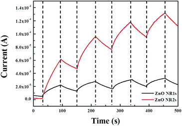 |
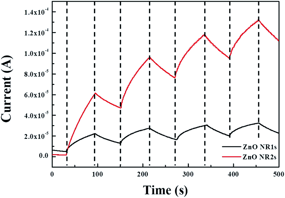
| | Fig. 9 Time-dependent UV photoresponse of ZnO NR1s and NR2s. | |
To confirm the possibility of using TDA method for the production of transparent and flexible optoelectronics, we fabricated a transparent and flexible MSM UV photodetectors from ZnO NRs grown on the two types of ZnO seed layers. Fig. 9 shows the time-dependent photoresponse of ZnO NRs measured by periodically turning on and off light (λ = 365 nm) with an interval of 60 s in air. The dark currents of ZnO NR1s and ZnO NR2s equalled 5.02 and 1.82 μA, respectively, while the respective photocurrents equalled 22.3 and 61.4 μA. The photocurrent difference was explained by considering the UV detection mechanism of ZnO NRs. The UV photoresponse of ZnO NRs could be divided into three steps, namely oxygen atom adsorption on the NR surface, oxygen ion desorption and the photogeneration of electron–hole pairs, and oxygen atom re-adsorption. As the first UV photoresponse process, when the ZnO NRs are held in the dark, oxygen atoms are adsorbed on the NR surface by capturing free electrons from the conduction band, which decreases the conductive region near the NR surface and increases the depletion region.68 In the second step (desorption of oxygen ions and photogeneration of electron–hole pairs) under UV illumination, photons with energies equal to or exceeding the band gap of ZnO NRs excite the electrons from the valence band to the conduction band to generate electron–hole pairs in ZnO NRs.69 At this point, some photogenerated holes move to the surface of ZnO thin films and combine with the electrons captured by oxygen atoms to reduce the depletion barrier near the NR surface. In contrast, the photogenerated electrons and the free electrons formed through the discharge of chemisorbed oxygen molecules migrate to the electrode under the bias voltage to increase photocurrent. After UV illumination, the photogenerated electron–hole pairs instantly recombine, and oxygen molecules are adsorbed on the NR surface to decrease the photocurrent.70 Thus, oxygen adsorption and desorption on/from the NR surface play important roles in UV photodetectors, and the surface area of ZnO NRs affects the increment in photocurrent, as a larger amount of oxygen atoms adsorbed and desorbed on/from the ZnO NR surface can increase the number of electrons and, hence, the photocurrent increment. Consequently, the lower dark current and higher photocurrent of ZnO NR2s with the annealed ZnO seed layer was explained by the largest amount of chemisorbed oxygen due to the highest density and larger surface area of ZnO NR2s, as discussed in the mechanism of UV photodetectors. Alternatively, the performance of ZnO-based UV photodetectors can be assessed in terms of the photosensitivity (S) and photoresponsivity (R) of ZnO NRs, which were calculated as
| | |
R = (Iph − Idark)/Pop,
| (4) |
where
Iph is the photocurrent,
Idark is the dark current, and
Pop is the optical power of UV light.
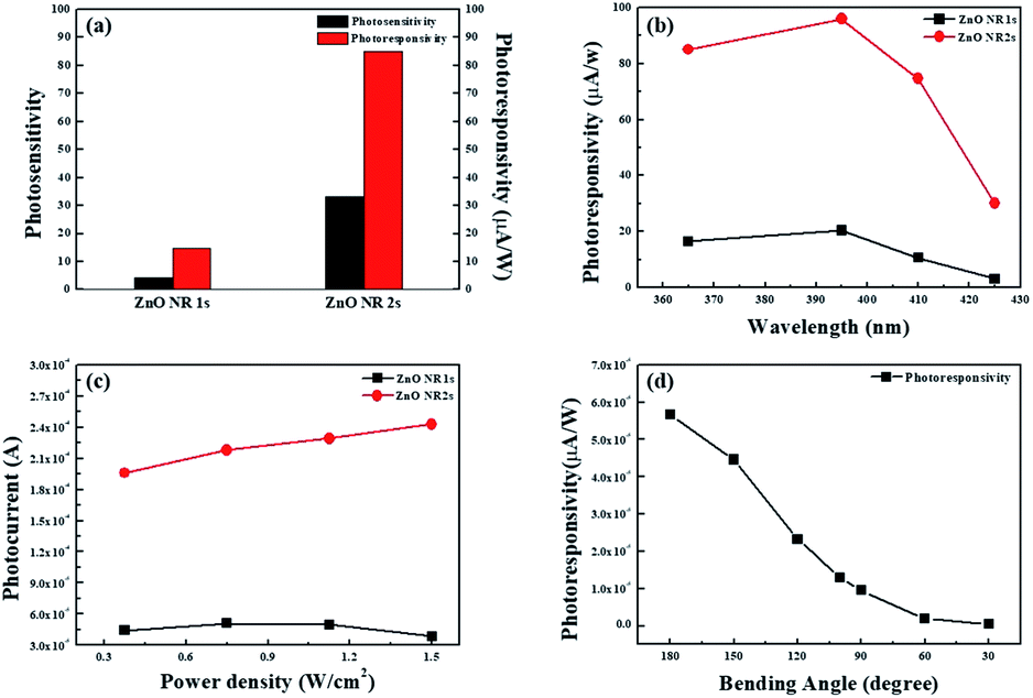
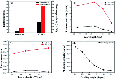
71,72 As shown in
Fig. 10(a), ZnO NR2s had a higher photosensitivity than ZnO NR1s,
i.e., more electrons were generated in the former NRs at the same UV exposure. Interestingly, ZnO NR2s also exhibited a two-fold higher photoresponsivity than ZnO NR1s. Unlike in the case of photosensitivity, photoresponsivity depends on the power of UV light and is defined as the amount of electrons generated through the discharge of chemisorbed oxygen molecules and photogeneration at a constant UV light power. In other words, more free electrons, formed by desorption of oxygen ions on the ZnO NR surface and from photogenerated electron–hole pairs, were generated on ZnO NR2s at the same exposure time and UV light power density because of the larger surface area and smaller number of defects that trapped free electrons and decreased the increment in photocurrent.
Fig. 10(b) and (c) shows the photoresponsivity and photocurrent changes of ZnO NRs at various wavelengths and power densities of UV light. As shown in
Fig. 10(b) and (c), ZnO NR2s exhibited a higher photocurrent than ZnO NR1s at all wavelengths and power densities. The photocurrents of ZnO NR1s and NR2s increased as the UV light wavelength increased from 365 to 395 nm, dramatically decreasing when the wavelength further increased to 425 nm. In general, the number of photogenerated electron–hole pairs is affected by the bandgap of ZnO NRs, as electrons can only be excited by photons with energies larger than that of the bandgap. Thus, the photocurrent at 365 nm exceeded that at 395 nm, as the former photons were more energetic. However, one should note that the PEN substrate used for the hydrothermal growth of ZnO NRs has a bandgap similar to that of ZnO NRs and thus absorbs a significant proportion of photon energy. In addition, the photocurrent of ZnO NR2s increased with increasing power density of UV light, whereas that of ZnO NR1s barely changed. The unlimited increase in photocurrent with increasing power density of UV light observed for ZnO NR2s was ascribed to their large surface area. Finally, a mechanical bending test was performed to evaluate the flexibility of the UV light detector fabricated using ZnO NR2s.
Fig. 10(d) shows the photocurrent of ZnO NRs during a static bending test at bending angles of 30 to 180° (flat state) at a power density of 0.375 mW cm
−2 and a bias of 1 V. As the bending angle changed from 180 to 150°, the photoresponsivity of ZnO NRs decreased from 55.6 to 44.6 μA W
−1, further decreasing with decreasing bending angle. Although the photoresponsivity of our flexible and transparent UV photodetectors decreased with decreasing bending angle, the photoresponsivity of ZnO NR2s bent at an angle of 90° exceeded that of ZnO NR1s in the flat state, which means that TDA can be used as an annealing method for the production of oxide semiconductor-based transparent and flexible optoelectronics.
 |
| | Fig. 10 (a) Photosensitivity and photoresponsivity of ZnO NR1s and NR2s, (b) photoresponsivity changes of ZnO NR1s and NR2s at various wavelengths of UV light, (c) photocurrent changes of ZnO NR1s and NR2s at various power densities of UV light, and (d) photoresponsivity. | |
4. Conclusions
ZnO NRs were hydrothermally grown on two types (annealed and non-annealed) of ZnO seed layers to investigate the effect of TDA method. ZnO NR2s, grown on the TDA-processed ZnO seed layer, exhibited a higher NR density than ZnO NR1s, which were grown on the non-annealed ZnO seed layer. Moreover, ZnO NR2s had a higher O 1s a peak intensity than ZnO NR1s, which was ascribed to the more pronounced recombination of the escaped Zn2+ ions and interstitial oxygen in the ZnO lattice in the latter case. Interestingly, all ZnO NRs featured a similar O 1sb peak intensity, which was attributed to the fact that the amount of oxygen vacancies was independent of growth conditions. ZnO NR2s exhibited a three-fold higher photocurrent than ZnO NR1s under the same measurement conditions. Moreover, the former NRs had a much higher photosensitivity and a three-fold higher photoresponsivity than the latter, which indicated that the TDA-induced crystallization of the ZnO seed layer is suitable for the growth of highly crystalline ZnO NRs. In addition, although the photoresponsivity of the flexible and transparent UV photodetectors fabricated using ZnO NR2s decreased with decreasing bending angle, the photoresponsivity of ZnO NR2s bent at an angle of 90° exceeded that of flat-state ZnO NR1s. Therefore, these results suggest that TDA is an effective method for the fabrication of transparent and flexible UV photodetectors with high photosensitivity, photoresponsivity, and photocurrent stability.
Conflicts of interest
There are no conflicts to declare.
Acknowledgements
This research was supported by the Basic Science Research Program through the National Research Foundation of Korea (NRF) funded by the Ministry of Education (No. 2018R1D1A1B07050792).
Notes and references
- J. Zhang, C. Wang and C. Zhou, ACS Nano, 2012, 6, 7412 CrossRef CAS PubMed.
- D.-Y. Kim, Y. C. Han, H. C. Kim, E. G. Jeong and K. C. Choi, Adv. Funct. Mater., 2015, 25, 7145 CrossRef CAS.
- S. Abbas, M. Kumar and J. Kim, Mater. Sci. Semicond. Process., 2018, 88, 86 CrossRef CAS.
- N. Liu, H. Tian, G. Schwartz, J. B.-H. Tok, T.-L. Ren and Z. Bao, Nano Lett., 2014, 14, 3702 CrossRef CAS PubMed.
- M.-A. Kang, S. Kim, I.-S. Jeon, Y. R. Lim, C.-Y. Park, W. Song, S. S. Lee, J. Lim, K.-S. An and S. Myung, RSC Adv., 2019, 9, 19707 RSC.
- Q. Humayun, M. Kashif, U. Hashim and A. Qurashi, Nanoscale Res. Lett., 2014, 9, 29 CrossRef PubMed.
- Y. Xie, L. Wei, G. Wei, Q. Li, D. Wang, Y. Chen, S. Yan, G. Liu, L. Mei and J. Jiao, Nanoscale Res. Lett., 2013, 8, 188 CrossRef PubMed.
- X. Bian, H. Jin, X. Wang, S. Dong, G. Chen, J. K. Luo, M. J. Deen and B. Qi, Sci. Rep., 2015, 5, 9123 CrossRef CAS PubMed.
- K. J. Lee, H. Oh, M. Jo, K. Lee and S. S. Yang, Microelectron. Eng., 2013, 111, 105 CrossRef CAS.
- Z. Zhang, Y. Ning and X. Fang, J. Mater. Chem. C, 2019, 7, 223 RSC.
- Z. Zhou, Y. Zhang, X. Chen, S. Li, Y. Zhao and X. Zhang, ACS Appl. Energy Mater., 2020, 3, 1574 CrossRef CAS.
- Y. Wang, J. Song, W. Song, Y. Tian, B. Han, X. Meng, F. Yang, Y. Ding and J. Li, Sol. Energy, 2019, 186, 126 CrossRef CAS.
- H. Zhang, W. Li, G. Qin, H. Ruan, Z. Huang, F. Wu, C. Kong and L. Fang, Appl. Surf. Sci., 2019, 492, 392 CrossRef CAS.
- Z. Yan, J. Bao, X.-Y. Yue, X.-L. Li, Y.-N. Zhou and X.-J. Wu, J. Alloys Compd., 2020, 812, 152093 CrossRef CAS.
- K. Kannan, D. Radhika, K. R. Reddy, A. V. Raghu, K. K. Sadasivuni, G. Palani and K. Gurushankar, Nano Express, 2021, 2, 010014 Search PubMed.
- K. Kannan, D. Radhika, A. S. Nesaraj, K. K. Sadasivuni, K. R. Reddy, D. Kasai and A. V. Raghu, Mater. Sci. Energy Technol., 2020, 3, 853 CAS.
- M. Srinivas, R. C. Venkata, R. R. Kakarla, N. P. Shetti, M. S. Reddy and V. R. Anjanapura, Mater. Res. Express, 2019, 6, 125502 CrossRef CAS.
- K. V. Karthik, C. V. Reddy, K. R. Reddy, R. Ravishankar, G. Sanjeev, R. V. Kulkarni, N. P. Shetti and A. V. Raghu, J. Mater. Sci.: Mater. Electron., 2019, 30, 5459 CrossRef.
- S. Inamdar, V. Ganbavle, S. Shaikh and K. Rajpure, Phys. Status Solidi A, 2015, 212, 1704 CrossRef CAS.
- H. Kim, M. D. Kumar, M. Patel and J. Kim, Mater. Res. Bull., 2016, 83, 35 CrossRef CAS.
- T. Ahmed and T. Edvinsson, J. Phys. Chem. C, 2020, 124, 6395 CrossRef CAS.
- J. Saghaei, A. Fallahzadeh and T. Saghaei, Sens. Actuators, A, 2016, 247, 150 CrossRef CAS.
- C. Barattoa, V. Golovanova, G. Faglia, H. Hakola, T. Niemi, N. Tkachenko, B. Nazarchurk and V. Golovanov, Appl. Surf. Sci., 2020, 528, 146959 CrossRef.
- L. Zhu, H. Li, Z. Liu, P. Xia, Y. Xie and D. Xiong, J. Phys. Chem. C, 2018, 122, 9531 CrossRef CAS.
- E. Cerrato, C. Gionco, M. C. Paganini, E. Giamello, E. Albanese and G. Pacchioni, ACS Appl. Energy Mater., 2018, 1, 4247 CrossRef CAS.
- D. Khim, Y.-H. Lin, S. Nam, H. Faber, K. Tetzner, R. Li, Q. Zhang, J. Li, X. Zhang and T. D. Anthopoulos, Adv. Mater., 2017, 29, 1605837 CrossRef PubMed.
- L. Zhu, Y. Li and W. Zeng, Appl. Surf. Sci., 2018, 427, 281 CrossRef CAS.
- S. Zhao, Y. Shen, X. Yan, P. Zhou, Y. Yin, R. Lu, C. Han, B. Cui and D. Wei, Sens. Actuators, B, 2019, 286, 501 CrossRef CAS.
- Y.-C. Yoon, K.-S. Park and S.-D. Kim, Thin Solid Films, 2015, 597, 125 CrossRef CAS.
- S. Guillemin, V. Consonni, E. Appert, E. Puyoo, L. Rapenne and H. Roussel, J. Phys. Chem. C, 2012, 116, 25106 CrossRef CAS.
- C. Wang, Chem. Phys. Lett., 2020, 749, 137471 CrossRef CAS.
- W. Lee and J.-Y. Leem, J. Nanosci. Nanotechnol., 2017, 17, 7952 CrossRef CAS.
- R. Das, A. Kumar, Y. Kumar, S. Sen and P. M. Shirage, RSC Adv., 2015, 5, 60365 RSC.
- Q. Fan, D. Li, J. Li and C. Wang, J. Alloys Compd., 2020, 829, 154483 CrossRef CAS.
- N. B. Patil, A. R. Nimbalkar and M. G. Patil, Mater. Sci. Eng., B, 2018, 227, 53 CrossRef CAS.
- M. R. Islam, M. Rahman, S. F. U. Farhad and J. Podder, Surf. Interfaces, 2019, 16, 120 CrossRef CAS.
- S. E. Ahn, J. S. Lee, H. Kim, S. Kim, B. H. Kang, K. H. Kim and G. T. Kim, Appl. Phys. Lett., 2004, 84, 5022 CrossRef CAS.
- L. Dejam, S. M. Elahi, H. H. Nazari, H. Elahi, S. Solaymani and A. Ghaderi, J. Mater. Sci.: Mater. Electron., 2016, 27, 685 CrossRef CAS.
- L. V. Gritsenko, K. A. Abdullin, M. T. Gabdullin, Z. K. Kalkozova, S. E. Kumekov, Z. O. Mukash, A. Y. Sazonov and E. I. Terukov, J. Cryst. Growth, 2017, 457, 164 CrossRef CAS.
- A. Umar, R. Kumar, G. Kumar, H. Algarni and S. H. Kim, J. Alloys Compd., 2015, 648, 46 CrossRef CAS.
- M. M. H. Farooqi and R. K. Srivastava, Proc. Natl. Acad. Sci., India, 2020, 90, 859 Search PubMed.
- Q. Xu, R. D. Hong, H. L. Huang, Z. F. Zhang, M. K. Zhang, X. P. Chen and Z. Y. Wu, Opt. Laser Technol., 2013, 45, 513 CrossRef CAS.
- G. Fiaschi, S. Mirabella, G. Franzò, L. Maiolo, A. Chitu, Y. Komem and Y. Shacham-Diamand, Appl. Surf. Sci., 2018, 458, 800 CrossRef CAS.
- H. Pan, N. Misra, S. H. Ko, C. P. Grigoropoulos, N. Miller, E. E. Haller and O. Dubon, Appl. Phys. A, 2009, 94, 111 CrossRef CAS.
- C. Charpentier, R. Boukhicha, P. Prod'homme, T. Emeraud, J.-F. Lerat, P. R. Cabarrocas and E. V. Johnson, Sol. Energy Mater. Sol. Cells, 2014, 125, 223 CrossRef CAS.
- Y. Kim and J.-Y. Leem, Mater. Chem. Phys., 2015, 167, 18 CrossRef CAS.
- D. Kim and J.-Y. Leem, Sci. Rep., 2021, 11, 382 CrossRef CAS PubMed.
- D. Kim and J.-Y. Leem, RSC Adv., 2021, 11, 876 RSC.
- P. Ariyakkani, L. Suganya and B. Sundaresan, J. Alloys Compd., 2017, 695, 3467 CrossRef CAS.
- J.-S. Park, I. Mahmud, H. J. Shin, M.-K. Park, A. Ranjkesh, D. K. Lee and H.-R. Kim, Appl. Surf. Sci., 2016, 362, 132 CrossRef CAS.
- T. You, J. Yan, Z. Zhang, J. Li, J. Tian, J. Yun and W. Zhao, Mater. Lett., 2012, 66, 246 CrossRef CAS.
- J. Xie, H. Wang, M. Duan and L. Zhang, Appl. Surf. Sci., 2011, 257, 6358 CrossRef CAS.
- Ş. Ş. Türkyılmaz, N. Güy and M. Özacara, J. Photochem. Photobiol., A, 2017, 341, 39 CrossRef.
- D. Upadhaya and D. D. Purkayastha, Ceram. Int., 2020, 46, 15731 CrossRef.
- D. A. Zatsepin, D. W. Boukhvalov, N. V. Gavrilov, E. Z. Kurmaev and I. S. Zhidkov, Appl. Surf. Sci., 2016, 387, 1093 CrossRef CAS.
- I. G. Morozov, O. V. Belousova, D. Ortega, M.-K. Mafina and M. V. Kuznetcov, J. Alloy. Compd., 2015, 633, 237 CrossRef CAS.
- A. Saáedi, R. Yousefi, F. Jamali-Sheini, A. K. Zak, M. Cheraghizade, M. R. Mahmoudian, M. A. Baghchesara and A. S. Dezaki, Phys. E, 2016, 79, 113 CrossRef.
- C. M. Pelicano and H. Yanahi, J. Mater. Chem. C, 2019, 7, 4653 RSC.
- B. Han, X. Liu, X. Xing, N. Chen, X. Xiao, S. Liu and Y. Wanga, Sens. Actuators, B, 2016, 237, 423 CrossRef CAS.
- L. K. Jangir, Y. Kumari, A. Kumar, M. Kumar and K. Awasthi, Mater. Chem. Front., 2017, 1, 1413 RSC.
- E. J. Guidelli, O. Baffa and D. R. Clarke, Sci. Rep., 2015, 5, 14004 CrossRef CAS PubMed.
- A. Rasool, M. C. S. Kumar, M. H. Mamat, C. Gopalakrishnan and R. Amiruddin, J. Mater. Sci.: Mater. Electron., 2020, 31, 7100 CrossRef CAS.
- J. Ji, A. M. Colosimo, W. Anwand, L. A. Boatner, A. Wagner, P. S. Stepanov, T. T. Trinh, M. O. Liedke, R. Krause-Rehberg, T. E. Cowan and F. A. Selim, Sci. Rep., 2016, 6, 31238 CrossRef CAS PubMed.
- E. Nurfani, M. A. K. Purbayanto, T. Aono, K. Takase and Y. Darma, Opt. Mater., 2018, 84, 453 CrossRef CAS.
- C. E. Kim, P. Moon, S. Kim, J.-M. Myoung, H. W. Jang, J. Bang and I. Yun, Thin Solid Films, 2010, 518, 6304 CrossRef CAS.
- R. S. Mohar, I. Sugihartono, V. Fauzia and A. A. Umar, Surf. Interfaces, 2020, 19, 100518 CrossRef CAS.
- H. Zaka, S. S. Fouad, B. Parditka, A. E. Bekheet, H. E. Atyia, M. Medhat and Z. Erdélyi, Sol. Energy, 2020, 205, 79 CrossRef CAS.
- V. Q. Dang, T. Q. Trung, D.-I. Kim, L. T. Duy, B.-U. Hwang, D.-W. Lee, B.-Y. Kim, L. D. Toan and N.-E. Lee, Small, 2015, 11, 3054 CrossRef CAS PubMed.
- K. Hu, F. Teng, L. Zheng, P. Yu, Z. Zhang, H. Chen and X. Fang, Laser Photonics Rev., 2017, 11, 1600257 CrossRef.
- T. Yang, B. Sun, L. Ni, X. Wei, T. Guo, Z. Shi, F. Han and L. Duan, Curr. Appl. Phys., 2018, 18, 859 CrossRef.
- A. Khayatian, M. A. Kashi, R. Azimirad, S. Safac and S. F. A. Akhtarian, Optik, 2016, 127, 4675 CrossRef CAS.
- Y. Zhang, X. Zhao, J. Chen, S. Li, W. Yang and X. Fang, Adv. Funct. Mater., 2020, 30, 1907650 CrossRef CAS.
Footnote |
| † Electronic supplementary information (ESI) available. See DOI: 10.1039/d1ra02578c |
|
| This journal is © The Royal Society of Chemistry 2021 |
Click here to see how this site uses Cookies. View our privacy policy here. 
 Open Access Article
 This Open Access Article is licensed under a Creative Commons Attribution-Non Commercial 3.0 Unported Licence
 *
*