DOI:
10.1039/D1RA02439F
(Paper)
RSC Adv., 2021,
11, 15632-15638
Dual-wavelength visible photodetector based on vertical (In,Ga)N nanowires grown by molecular beam epitaxy†
Received
27th March 2021
, Accepted 12th April 2021
First published on 27th April 2021
Abstract
Due to the wide applications of blue and red photodetectors, dual-wavelength (blue/red) photodetectors are promising for future markets. In this work, a dual-wavelength photodetector based on vertical (In,Ga)N nanowires and graphene has been fabricated successfully. By using the transparent graphene, both blue and red responses can be clearly detected. The rise time of response can reach 3.5 ms. Furthermore, the underlying mechanism of double responses has also been analyzed. The main reason contributing to the dual-wavelength response could be the different diameters of nanowires, leading to different In components within (In,Ga)N sections.
1. Introduction
Due to the high data rate, enhanced security, energy efficiency and less vulnerable to electromagnetic interference, visible light communication (VLC) has attracted more and more attention.1–3 With the gradually increasing demands in wireless light communication, some reports have demonstrated using photoelectronic devices in VLC systems.4–8 On the other hand, dual-wavelength photodetectors are beneficial to increase the accuracy by reducing false positive detection.9 In general, dual detectors are needed for the detection of dual-wavelength bands, which not only increase the manufacturing cost, but also put forward high requirements for system assembly and compatibility.9 Hence, a single light detector with dual-wavelength response is necessary to solve above problems. Besides reducing mine detection errors, dual-wavelength photodetector can provide more solutions for imaging, sensing, optical communication, flame monitoring and other fields in the future.9–11 However, very few publications have been reported about the research of dual-wavelength detection in visible band.
(In,Ga)N is an ideal material for visible detectors because of its direct and adjustable band gap (0.7–3.4 eV).12 At present, GaN-based detectors are mostly based on thin film and bulk materials.2,13,14 Compared with thin films or bulk materials, nanowires (NWs) have larger surface-to-volume ratio, which will increase optical absorption and photogenerated carrier density.15,16 However, very few detectors are based on vertical nanowires, not to mention the corresponding dual-wavelength photodetector.17 In our previous work, a UV detector based on (Al,Ga)N nanowires only achieved a single response in the UV range.18,19 Therefore, the research of (In,Ga)N dual-wavelength detectors is promising but still faces great challenges.
In this work, we fabricated a dual-wavelength detector based on (In,Ga)N/GaN nanowires. The maximum responsivities at dual ranges are both over 20 mA W−1. Graphene was utilized as a current collecting layer for the good transparency and conductivity. The underlying mechanism contributing to the double responses has been studied systematically.
2. Experimental section
2.1 Preparation of (In,Ga)N nanowires
Prior to the molecular beam epitaxy (MBE, Vecco G20) growth, the Si (111) substrates in the growth chamber should be heated up to about 900 °C for 15 min to eliminate native oxides by observing the 7 × 7 reconstruction. Initially, a ∼3.0 nm buffer layer of AlN was grown. Subsequently, GaN nanowires were grown with a Ga flux of ∼2.0 × 10⁻⁸ torr for about 2 hours. The substrate temperature is set to be 770 °C. The deposited GaN initially forms into islands which act as a material collector and a seed for the nanowires.18 After the growth of GaN section, the (In,Ga)N section was grown for 60 min with a growth rate of ∼2.0 nm min−1. For a better In incorporation, the substrate temperature was decreased from 770 °C to 650 °C with an In/Ga flux ratio of ∼3.7. When starting and finishing growing the (In,Ga)N segment, the shutters of In and Ga cells were opened and closed simultaneously controlled by the software. Finally, a thin GaN cap was grown for 30 min with a growth rate of ∼1.7 nm min−1. To increase the nanowire uniformity, samples were rotated with a rate of 120° s−1 during the growth process.
2.2 Fabrication of photodetector
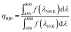
To fabricate the photodetectors, a ∼200 nm-thick SiO2 film was deposited on the top of nanowires as an insulating layer by means of inductively coupled plasma chemical vapour deposition (ICPCVD). Then the SiO2 film was selectively removed by photolithography to expose some nanowires. Graphene was used as a transparent current collecting layer on the top of nanowires. The transfer of graphene was carried out by etching the copper foil with the assistance of polymethyl methacrylate (PMMA). The specific processes are shown in Fig. S1 (ESI†). Finally, Ti/Pt/Au film was deposited on the graphene surface as an electrode. After that, Ti/Al (50/200 nm) film was deposited on the backside of the Si substrate by electron beam evaporation.
2.3 Characterization methods
To characterize the surface morphology and element distribution of nanowires, scanning electron microscopy (SEM, S-4800, HITACHI) and scanning transmission electron microscopy (STEM, Talos F200x, FEI) with a high-resolution energy dispersive X-ray (EDX) mapping were used. Focused ion beam (FIB, Scios, FEI) was utilized to prepare the STEM samples. To make nanowires more stable during the FIB preparation process, the carbon layer covered by electron beam assisted deposition is thicker (∼200 nm) than normal (∼50 nm).20 More details can be found in ref. 20.
The current–voltage (I–V) and transient responses characteristics of the (In,Ga)N photodetectors were measured by the probe station (Agilent B1500A). The detection time accuracy of the instrument is set to be 2 ms. Relay switch was used to adjust the on/off time of lighting LED, and the time step of lighting switch is 1 s. The spectral response measurement was employed by a self-constructed photoelectric measurement system mainly consisting of an optical chopper, a xenon lamp (ABET Technologies) and a power supply.
3. Result and discussion
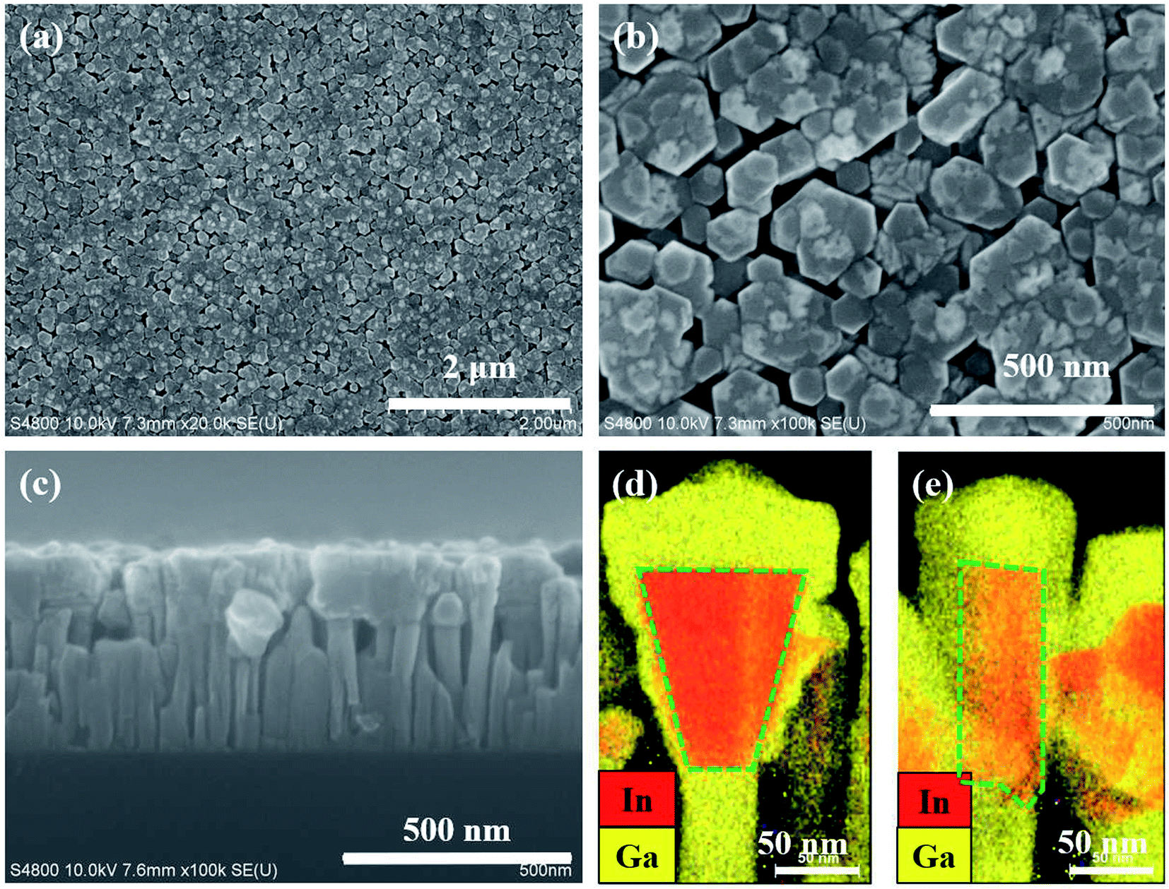
3.1 SEM and STEM analyses of (In,Ga)N nanowires
From the top-view and side-view SEM images in Fig. 1, the nanowires are formed and distributed on the Si substrate with good verticality. It is known that such self-assembled GaN nanowires grow in the N-polar direction,21–23 which result in negligible polarity variations between nanowires. The dense nanowires have small blank space among nanowires, which are beneficial to solidify nanowires during the processes of fabricating detector, such as photolithography and cleaning processes. As shown in Fig. 1(d) and (e), vertical (In,Ga)N sections have been fabricated as designed. The lateral surface of (In,Ga)N segment is wrapped by GaN section, forming a core–shell structure. For the higher accuracy, we integrated the In/Ga EDX intensities of an (In,Ga)N section instead of a linear scanning. Compared the surface integrations within the green dotted frames in Fig. 1(d) and (e), the In/Ga ratio of thick (In,Ga)N section is larger than that of thin (In,Ga)N section. Therefore, the In component of thick nanowires is expected to be higher than that of the thin nanowire.
 |
| | Fig. 1 (a) and (b) Top-view and (c) side-view SEM images of vertical (In,Ga)N nanowires. The high-resolution EDX mapping of (d) thick and (e) thin (In,Ga)N nanowires. | |
3.2 Optical properties of nanowires and photodetector structure
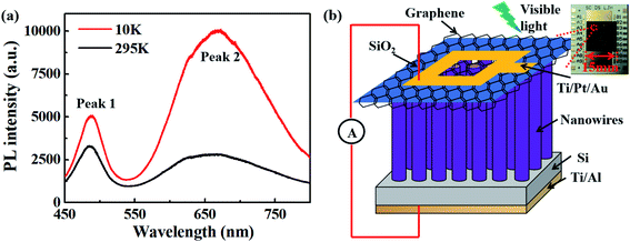
As shown in Fig. 2(a), two photoluminescence (PL) peaks of (In,Ga)N nanowires can be clearly measured at both 10 K and 295 K. The wavelength of excitation light used in PL test is 405 nm. Fig. 2(b) shows a schematic diagram of the detector under the measurement of responsiveness. When testing responsiveness, a bias of −2 V is applied to the detector.
 |
| | Fig. 2 (a) PL spectra of (In,Ga)N nanowires measured at 10 K and 295 K. (b) The optical image of photodetectors and the schematic diagram of one detector. | |
By comparing those at 10 K and 295 K, the peaks remain stable, which indicate that the epitaxial stresses have been significantly released in the nanowires. As peak 2 still exists at 10 K, which demonstrates that it comes from the (In,Ga)N section, not the defects. According to physical properties with Vegard's law,24 the band gap of InxGa1−xN is calculated by the following equation:
| | |
Eg(InxGa1−xN) = xEg(InN) + (1 − x)Eg(GaN) − bx(1 − x)
| (1) |
where
b is the bowing parameter of (In,Ga)N. According to the published paper,
b is selected as 1.43 eV,
25 the band gap of InN is 0.7 eV, GaN is 3.4 eV.
12 From
eqn (1), the In components of as-grown (In,Ga)N nanowires at 295 K corresponding to the peak 1 (∼485 nm) and peak 2 (∼667 nm) in
Fig. 2(a) are ∼22% and ∼44%, respectively.
In addition, we use the ratio of the integral area of the PL spectra at both 295 K and 10 K [eqn (2)] to calculate the internal quantum efficiency (IQE, ηIQE).
| |
 | (2) |
f(
λ295 K) and
f(
λ10 K) represent the PL curves at 295 K and 10 K, respectively. The IQE and external quantum efficiency (EQE) of (In,Ga)N devices should increase rapidly and then decrease with the increase of current density, which normally regarded as “Efficiency droop”.
26,27 To simplify the calculation, the current density corresponding to maximum EQE or IQE is set as 5 A cm
−2.
26 It is assumed that each electron can excite a photon, which means an electron corresponds to a photon. Therefore, the light power (
P) of the excitation source (PL laser) corresponding to the current density (5 A cm
−2) for maximum EQE or IQE can be calculated by the following equations.
| |
 | (3) |
| |
 | (4) |
Q is the amount of charge passing through an area of
S (1 cm
2) per unit time (1 s),
j is the current density,
e is the electron charge,
M is the number of electrons.
E is the energy of a single photon.
h is the Planck constant.
c is the speed of light.
λ is the wavelength of the laser source. The spot area of laser on the sample (
S′) was about 0.005 cm
2. By calculation, the power of the laser source (
P) is about 77 mW. The practical incident laser power in our experiment (∼14 mW) is much less than 77 mW. It is pretty difficult to obtain such maximum IQE because of the lack of high-power laser. By simulating the PL data from 450 nm to 800 nm based on
eqn (2), the IQE is ∼38%. Therefore, the actual maximum IQE should be higher than 38%.
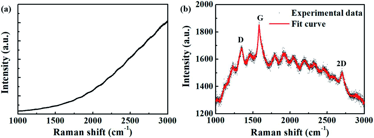
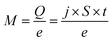
Fig. 3 shows the Raman spectra of as-grown nanowires and graphene detected by an excitation wavelength of 532 nm. D peak (∼1347 cm−1) is used to represent defects, and G peak (∼1585 cm−1) is caused by the plane vibration of the sp2 hybrid carbon atom.18 The quality of graphene is characterized by the ratio of the peak value of G and the peak value of D (IG/ID). For sp2 hybrid carbon materials, 2D peak (∼2699 cm−1) is produced by two phonons resonance, corresponding to the coupling of two opposite wave vector photons at Brillouin boundary. Fig. 3 proves that the D, G and 2D peaks come from the graphene, not the nanowires. Hence, graphene exists when the device fabrication completed. Moreover, the ratio of peak intensity (I2D/IG) reflects the number of graphene layers. It has been reported that the ratio of I2D/IG is less than 2, indicating that graphene is multilayered.18 As shown in Fig. 3(b), this ratio of the sample is 0.81, which means the graphene is multilayered.
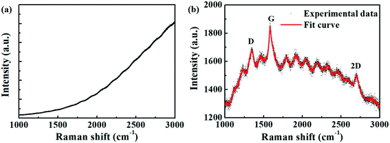 |
| | Fig. 3 Raman spectra of (a) the as-grown nanowires without graphene and (b) the graphene on the top of nanowires. | |
3.3 Performance and analysis of photodetector
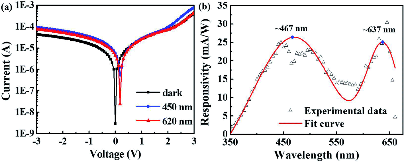
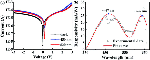
The I–V characteristics of the detector were measured in dark and 450 nm/620 nm illuminations. As shown in Fig. 4(a), the I–V curves of the detector under no illumination are nonlinear, which indicates that Schottky contact exists between graphene and nanowires.28 In addition, the dark current of the detector is about 44 μA at −3 V with an area of ∼0.46 mm2. The spectral responsivity of the detector is defined as the photocurrent output under the action of the unit incident radiation power.29 Fig. 4(b) clearly illustrates that the detector shows a dual-wavelength response in the band of 400–700 nm. The maximum responsivity of the first response in the range of blue band (467 nm) is around 26 mA W−1, while that of the second response in the range of red band (637 nm) is about 25 mA W−1.
 |
| | Fig. 4 (a) Current–voltage characteristics of detector measured in dark and 450 nm/620 nm illuminations. (b) Spectral response of the detector at the bias of −2 V. | |
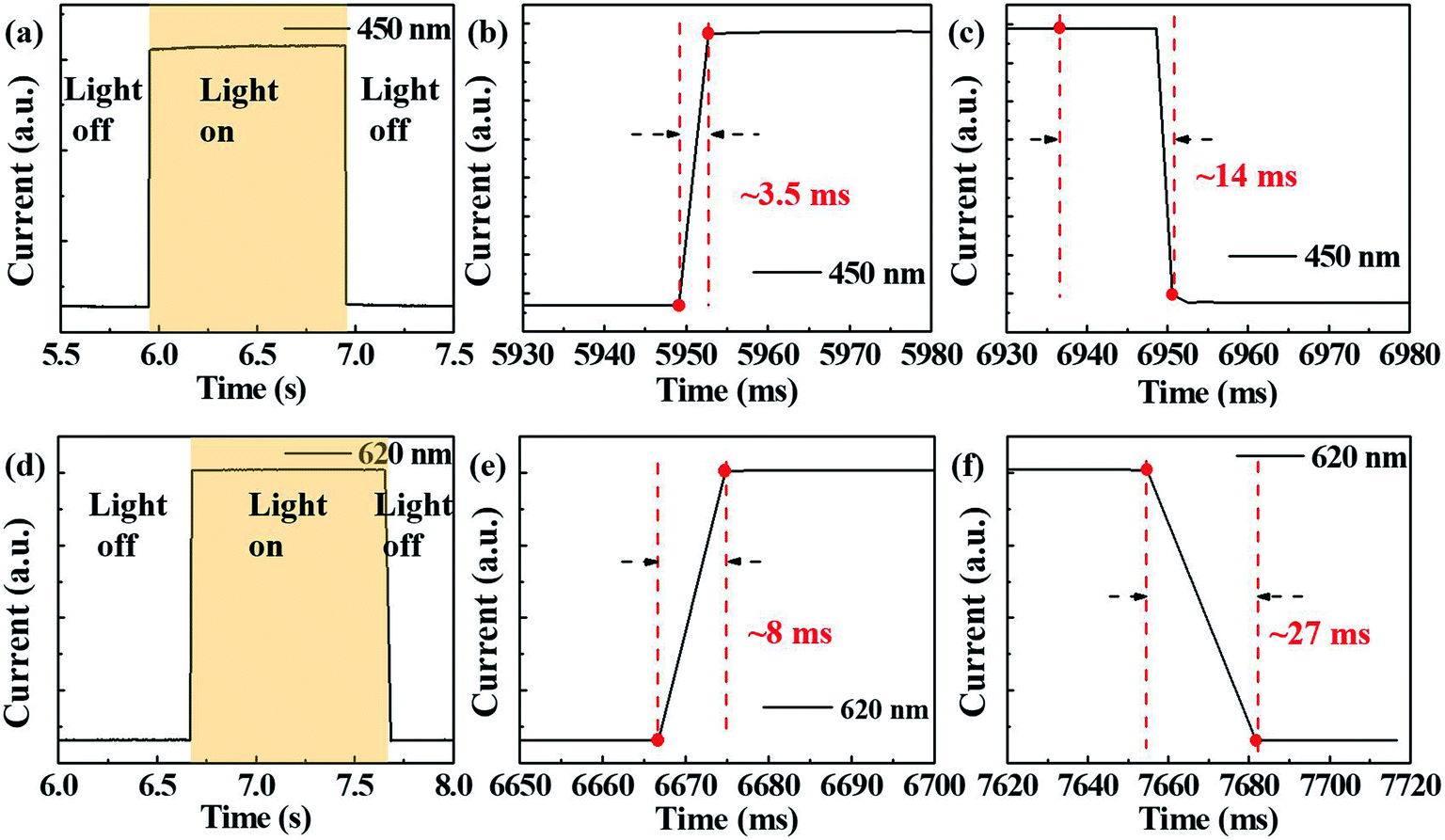
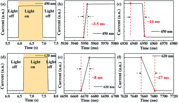
Fig. 5 shows the current switching characteristics of the detector under 450 nm and 620 nm illumination at −2 V, corresponding to the first and second responses, respectively. All measurements have been conducted at room temperature in air. The on/off current can increase/decrease in a certain period of time with/without irradiations. The rise time (trise) is around 3.5 ms and 8 ms and the decay time (tfall) is about 14 ms and 27 ms at 450 nm and 620 nm illumination, respectively. In order to better compare with some recent novel photodetectors, Table 1 lists the key parameters. By comparison, this work has the advantages in the transient response.
 |
| | Fig. 5 (a) Transient blue response of the detector under 450 nm illumination. (b) Enlarged view of detector rise time under 450 nm illumination. (c) Enlarged view of detector fall time under 450 nm illumination. (d) Transient red response of the detector under 620 nm illumination. (e) Enlarged view of detector rise time under 620 nm illumination. (f) Enlarged view of detector fall time under 620 nm illumination. | |
Table 1 Comparison of response time between this work and some state-of-the-art reports
| Material |
Response wavelength (nm) |
trise (ms) |
tfall (ms) |
Ref. |
| CsPbBr3NCs/graphene |
532 |
7.9 |
125 |
30 |
| 0.1 M CdS |
532 |
200 |
300 |
31 |
| CH3NH3PbI3 |
895 |
220 |
160 |
32 |
| Graphene/ZnO NWs/Si |
480 |
1.48 × 10⁻⁶ |
1.27 × 10⁻⁶ |
33 |
| Au/Bi2O2Se/Au |
532 |
2.4 × 10⁻² |
80 |
34 |
| MoS2/GaN |
405 |
1360 |
8310 |
35 |
| (In,Ga)N/GaN NWs |
450 |
3.5 |
14 |
This work |
| 620 |
8 |
27 |
This work |
The nanowire diameters can affect the In component, which leads to the multiple-peaked distribution of PL spectra in Fig. 2(a).36–38 To further study the underlying mechanism, Fig. 6 displays the kinetic processes such as atomic impinge, adsorption, diffusion and desorption. Atomic flux (Φ) expresses the atomic quantity per unit surface and unit time. Φtop,impinge and Φtop,desorption mean the impinging flux and desorption loss at top surface, respectively. Φside,impinge and Φside,desorption represent the impinging flux and desorption loss at sidewall, respectively. The comprehensive equations for effectively-adsorbed atomic flux (Φeff) are calculated under a steady state growth as follows.39
| | |
Φtop,eff = Φtop,impinge + Φdiff − Φtop,desorption
| (5) |
| | |
Φside,eff = Φside,impinge − Φdiff − Φside,desorption
| (6) |
Φdiff is the diffusion flux from sidewall to top surface. As the space among nanowires is quite small, few impinging fluxes can reach the nanowire sidewalls. That means a large amount of In, Ga and N atoms are blocked because of the shadow effect of nanowires. Furthermore, as the nanowire height is much larger than nanowire diameter (
Fig. 1),
Φside,eff should be much smaller than
Φtop,eff (
Φside,eff ≪
Φtop,eff) and
Φdiff should be minimal. Thus,
Φtop,eff has a much more significant effect on the growth of (In,Ga)N section than
Φside,eff. In addition, during the MBE growth,
Φtop,impinge can be regarded as a constant for all nanowires. When the nanowire diameter becomes larger, In atoms need more energy and time to diffuse or desorb from the (In,Ga)N section, which may result in that more In atoms remain. Therefore,
Φtop,eff of In atoms could be larger for the nanowires with larger diameters. The (In,Ga)N nanowire with a larger diameter is more likely to have a higher In component.
40,41
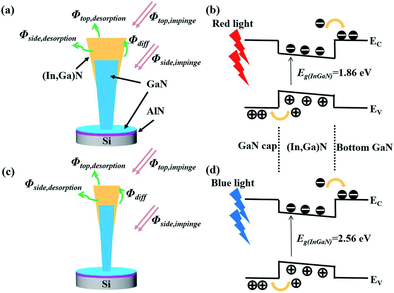
Fig. 1 clearly illustrates that nanowires with both thick and thin diameters can be grown by MBE simultaneously. In order to further study the underlying mechanism of dual-wavelength detector, we plot the schematic diagrams of structures and energy bands in Fig. 6. At −2 V bias voltage, when red/blue light irradiates on the photodetector (Fig. 2(b)), photons can reach the nanowires through the graphene as it is thin enough and transparent in the visible range. Then, photons can be absorbed by (In,Ga)N sections. As illustrated in Fig. 6(b) and (d), electrons in the valence band are excited to the conduction band, producing electron–hole pairs. Therefore, when exposed to the illuminations, nanowires with thick diameters play a key role in the red response (Fig. 6(b)), while thin nanowires have the main effect on blue response (Fig. 6(d)).
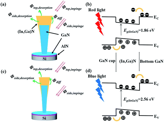 |
| | Fig. 6 Schematic diagrams of (In,Ga)N sections with (a) a thick diameter and (c) a thin diameter. Energy band diagram of the (In,Ga)N nanowires under the (b) red illumination and (d) blue illumination. | |
4. Conclusion
In summary, we demonstrate a dual-wavelength (red/blue) photodetector based on vertical (In,Ga)N/GaN nanowires grown by MBE. By using the transparent graphene, the maximum responsivity of blue band is ∼26 mA W−1, while that of the second response in the range of red band is ∼25 mA W−1. Moreover, different nanowire diameters can lead to different In components within (In,Ga)N sections, which could be the main parameter contributing to the dual-wavelength response. It is pretty promising for promoting the development of dual-wavelength detectors based on vertical nanowires.
Conflicts of interest
The authors declare no conflict of interest.
Acknowledgements
The authors are grateful for National Key Research and Development Program of China (No. 2018YFB0406602), Natural Science Foundation of Jiangsu Province (No. BK20180252), Key Research and Development Program of Jiangsu Province (No. BE2018005), Key Research Program of Frontier Sciences, CAS (No. ZDBS-LY-JSC034), and National Natural Science Foundation of China (No. 61804163 and 61875224). The authors also would like to acknowledge the support from Natural Science Foundation of Jiangxi Province (No. 20192BBEL50033) and Research Program of Scientific Instrument and Equipment of CAS (No. YJKYYQ20200073). We are thankful for the technical support from Vacuum Interconnected Nanotech Workstation (Nano-X, No. B2006), Platform for Characterization & Test of SINANO, CAS.
References
- J. Li, C. Yang, L. Liu, H. Cao, S. Lin, X. Xi, X. Li, Z. Ma, K. Wang, A. Patane and L. Zhao, Adv. Opt. Mater., 2020, 8, 1901276 CrossRef CAS.
- X. Liu, R. Lin, H. Chen, S. Zhang, Z. Qian, G. Zhou, X. Chen, X. Zhou, L. Zheng, R. Liu and P. Tian, ACS Photonics, 2019, 6, 3186–3195 CrossRef CAS.
- S. Mei, X. Liu, W. Zhang, R. Liu, L. Zheng, R. Guo and P. Tian, ACS Appl. Mater. Interfaces, 2018, 10, 5641–5648 CrossRef CAS PubMed.
- C. Du, C. Jiang, P. Zuo, X. Huang, X. Pu, Z. Zhao, Y. Zhou, L. Li, H. Chen, W. Hu and Z. L. Wang, Small, 2015, 11, 6071–6077 CrossRef CAS PubMed.
- C. Gong, Electronics, 2019, 8, 788 CrossRef.
- M. H. A. K. Khushik and C. Jiang, Curr. Opt. Photonics, 2019, 3, 105–110 CAS.
- P. H. Pathak, X. Feng, P. Hu and P. Mohapatra, IEEE Commun. Surv. Tutorials, 2015, 17, 2047–2077 Search PubMed.
- L. Y. Wei, Y. Liu, C. W. Chow, G. H. Chen, C. W. Peng, P. C. Guo, J. F. Tsai and C. H. Yeh, Electron. Lett., 2020, 56, 945–946 CrossRef.
- G. Ariyawansa, M. B. M. Rinzan, S. G. Matsik, G. Hastings, A. G. U. Perera, H. C. Liu, M. Buchanan, G. I. Sproule, V. I. Gavrilenko and V. P. Kuznetsov, Appl. Phys. Lett., 2006, 89, 061112 CrossRef.
- A. M. Chowdhury, G. Chandan, R. Pant, B. Roul, D. K. Singh, K. K. Nanda and S. B. Krupanidhi, ACS Appl. Mater. Interfaces, 2019, 11, 10418–10425 CrossRef CAS PubMed.
- A. Aiello, A. K. M. H. Hoque, M. Z. Baten and P. Bhattacharya, ACS Photonics, 2019, 6, 1289–1294 CrossRef CAS.
- F. Rasouli and Z. Hemmat, Opt. Quantum Electron., 2016, 48, 23 CrossRef.
- C. J. Lee, C. H. Won, J. H. Lee, S. H. Hahm and H. Park, Sensors, 2017, 17, 1684 CrossRef PubMed.
- R. Pillai, D. Starikov, J. Gandhi, A. Debnath, R. T. Li, C. Boney and A. Bensaoula, J. Vac. Sci. Technol., B: Nanotechnol. Microelectron.: Mater., Process., Meas., Phenom., 2015, 33, 011205 Search PubMed.
- Y. Zheng, W. Wang, Y. Li, J. Lan, Y. Xia, Z. Yang, X. He and G. Li, ACS Appl. Mater. Interfaces, 2019, 11, 13589–13597 CrossRef CAS PubMed.
- X. Zhang, H. Lourenco-Martins, S. Meuret, M. Kociak, B. Haas, J. L. Rouviere, P. H. Jouneau, C. Bougerol, T. Auzelle, D. Jalabert, X. Biquard, B. Gayral and B. Daudin, Nanotechnology, 2016, 27, 195704 CrossRef PubMed.
- T. He, Y. Zhao, X. Zhang, W. Lin, K. Fu, C. Sun, F. Shi, X. Ding, G. Yu, K. Zhang, S. Lu, X. Zhang and B. Zhang, Nanophotonics, 2018, 7, 1557–1562 CAS.
- M. Zhou, H. Qiu, T. He, J. Zhang, W. Yang, S. Lu, L. Bian and Y. Zhao, Phys. Status Solidi A, 2020, 217, 2000061 CrossRef CAS.
- Z. Xing, Y. Zhao, L. Bian, J. Zhang, M. Zhou, W. Yang, Y. Wu, M. Jiang, J. Long and S. Lu, Mater. Adv., 2021, 2, 1006–1015 RSC.
- S. J. Haigh, A. Gholinia, R. Jalil, S. Romani, L. Britnell, D. C. Elias, K. S. Novoselov, L. A. Ponomarenko, A. K. Geim and R. Gorbachev, Nat. Mater., 2012, 11, 764–767 CrossRef CAS PubMed.
- S. Fernandez-Garrido, X. Kong, T. Gotschke, R. Calarco, L. Geelhaar, A. Trampert and O. Brandt, Nano Lett., 2012, 12, 6119–6125 CrossRef CAS PubMed.
- T. Auzelle, B. Haas, A. Minj, C. Bougerol, J.-L. Rouviere, A. Cros, J. Colchero and B. Daudin, J. Appl. Phys., 2015, 117, 245303 CrossRef.
- M. D. Brubaker, S. M. Duff, T. E. Harvey, P. T. Blanchard, A. Roshko, A. W. Sanders, N. A. Sanford and K. A. Bertness, Cryst. Growth Des., 2016, 16, 596–604 CrossRef CAS.
- A. R. Denton and N. W. Ashcroft, Phys. Rev. A: At., Mol., Opt. Phys., 1991, 43, 3161–3164 CrossRef CAS PubMed.
- J. Wu, W. Walukiewicz, K. M. Yu, J. W. Ager, E. E. Haller, H. Lu and W. J. Schaff, Appl. Phys. Lett., 2002, 80, 4741–4743 CrossRef CAS.
- Z. Chen, S. Yan and C. Danesh, J. Phys. D: Appl. Phys., 2021, 54, 123001 CrossRef CAS.
- Y. Zhao, F. Yun, S. Wang, L. Feng, X. Su, Y. Li, M. Guo, W. Ding and Y. Zhang, Jpn. J. Appl. Phys., 2017, 56, 062101 CrossRef.
- C. A. Hernández-Gutiérrez, Y. Kudriavtsev, D. Cardona, A. G. Hernández and J. L. Camas-Anzueto, Opt. Mater., 2021, 111, 110541 CrossRef.
- Y. Huang, L. Zhang, J. Wang, X. Chu, D. Zhang, X. Zhao, X. Li, L. Xin, Y. Zhao and F. Zhao, J. Alloys Compd., 2019, 802, 70–75 CrossRef CAS.
- Y. Che, X. Cao, Y. Zhang and J. Yao, J. Mater. Sci., 2021, 56, 2341–2346 CrossRef CAS.
- M. D. Devi, A. V. Juliet, K. H. Prasad, T. Alshahrani, A. M. Alshehri, M. Shkir and S. AIFaify, Appl. Phys. A: Mater. Sci. Process., 2020, 126, 960 CrossRef CAS.
- J. Xin, Q. Wang, J. Li, K. Wang, W. Deng, J. Jin, M. Peng, M. Fang, J. Qu and H. Wang, J. Phys. D: Appl. Phys., 2020, 53, 414003 CrossRef CAS.
- S. Bansal, K. Prakash, K. Sharma, N. Sardana, S. Kumar, N. Gupta and A. K. Singh, Nanotechnology, 2020, 31, 405205 CrossRef CAS PubMed.
- T. Tong, W. Li, S. Qin, X. Yuan, Y. Chen, C. Zhang, W. Liu, P. Wang, W. Hu, F. Wang, J. Zhang, R. Zhang and Y. Xu, IEEE Electron Device Lett., 2020, 41, 1464–1467 CAS.
- Y. Wu, Z. Li, K.-W. Ang, Y. Jia, Z. Shi, Z. Huang, W. Yu, X. Sun, X. Liu and D. Li, Photonics Res., 2019, 7, 1127–1133 CrossRef CAS.
- W. Shan, W. Walukiewicz, E. E. Haller, B. D. Little, J. J. Song, M. D. McCluskey, N. M. Johnson, Z. C. Feng, M. Schurman and R. A. Stall, J. Appl. Phys., 1998, 84, 4452–4458 CrossRef CAS.
- Y. Zhao, Z. Xing, L. Geelhaar, J. Zhang, W. Yang, T. Auzelle, Y. Wu, L. Bian and S. Lu, ACS Appl. Nano Mater., 2020, 3, 9943–9950 CrossRef CAS.
- A. L. Bavencove, G. Tourbot, J. Garcia, Y. Desieres, P. Gilet, F. Levy, B. Andre, B. Gayral, B. Daudin and L. S. Dang, Nanotechnology, 2011, 22, 345705 CrossRef CAS PubMed.
- Y. Zhao, W. Yang, S. Lu, Y. Wu, X. Zhang, L. Bian, X. Li and M. Tan, J. Cryst. Growth, 2019, 514, 124–129 CrossRef CAS.
- X. Zhang, B. Haas, J.-L. Rouviere, E. Robin and B. Daudin, Nanotechnology, 2016, 27, 455603 CrossRef PubMed.
- M. Spies, J. Polaczynski, A. Ajay, D. Kalita, M. A. Luong, J. Lahnemann, B. Gayral, M. I. den Hertog and E. Monroy, Nanotechnology, 2018, 29, 255204 CrossRef PubMed.
Footnote |
| † Electronic supplementary information (ESI) available. See DOI: 10.1039/d1ra02439f |
|
| This journal is © The Royal Society of Chemistry 2021 |
Click here to see how this site uses Cookies. View our privacy policy here. 
 Open Access Article
 This Open Access Article is licensed under a Creative Commons Attribution-Non Commercial 3.0 Unported Licence
 *a,
Hua Qinab,
Wenxian Yanga,
Yuanyuan Wua,
Zhiwei Xingab and
Shulong Lu*ab
*a,
Hua Qinab,
Wenxian Yanga,
Yuanyuan Wua,
Zhiwei Xingab and
Shulong Lu*ab