
 Open Access Article
 This Open Access Article is licensed under a Creative Commons Attribution-Non Commercial 3.0 Unported Licence
Comparison of surface-passivation ability of the BAI salt and its induced 2D perovskite for high-performance inverted perovskite solar cells
Hanhong Zhang†a,
Song Wang†
a,
Youzheng Houa,
Fan Zhang *a,
Yuying Haoc,
Jun Songa and
Junle Quab
*a,
Yuying Haoc,
Jun Songa and
Junle Quab
aCenter for Biomedical Optics and Photonics (CBOP), College of Physics and Optoelectronic Engineering, Key Laboratory of Optoelectronic Devices and Systems, Shenzhen University, Shenzhen, 518060, P. R. China. E-mail: fanzhang@szu.edu.cn
bNational Research Nuclear University MEPhI (Moscow Engineering Physics Institute), 115409, Moscow, Russian Federation
cTaiyuan University of Technology, Taiyuan, 030024, China
First published on 1st July 2021
Abstract
Organic–inorganic lead halide perovskite solar cells have shown a rapid increase in power conversion efficiency (PCE) in the past decade. However, their performance still suffers from trap-assisted decline due to defects at the surface and grain boundaries in the polycrystalline active layer. In this study, a thin BAI layer was formed on the CH3NH3PbI3 surface, which was then transformed into either a two-dimensional (2D) perovskite layer (BA2PbI4) or the organic salt itself by controlling the post-annealing process. A variety of characterization results show that the 2D perovskites could effectively reduce the trap-assisted charge recombination and increase the device stability. Therefore, a remarkably enhanced PCE of 20.6% was achieved in the modified inverted perovskite solar cells.
1 Introduction
Hybrid organic–inorganic perovskite solar cells (PSCs) have attracted significant attention due to their rapidly increasing power conversion efficiency (PCE), which is now over 25.2% with certification.1–8 Such a high PCE has been achieved as a result of extensive research on perovskite composition adjustment,9–13 film crystallization optimization,14,15 and interfacial engineering.16–20 The efficiency limit of CH3NH3PbI3 perovskite solar cells without defect restriction is estimated to be 31%,21 which means that the current performance is still far below its ceiling.22–24Passivation of the surface defects has been proved to be necessary for all types of solar cells.25,26 Extensive research effort has been devoted to obtaining efficient passivation of defects present on solar cells. For example, an insulating layer at the perovskite surface consisting of polystyrene (PS),18 poly (methyl methacrylate) (PMMA), and poly(ethylene glycol) (PEG), and a charge transport layer are typically generated to suppress surface recombination and increase the VOC.27–30 The insulating passivation layer should be adequately thin to allow charge tunneling. Two-dimensional (2D) perovskite materials, such as PEA2PbI4 and BA2PbI4, have been formed as a graded 2D–3D structure, which advantageously modifies the surface states of the perovskite films.31 Due to the protection offered by organic ligands, 2D perovskites are more stable than 3D perovskite materials. This work describes a method for fabricating a 2D/3D structure by reacting a 3D perovskite with ammonium iodide butyrate (BAI).20 The reaction of BAI with PbI2 produces BA2PbI4. Since there are more organic ligands in BA2PbI4 than in the mixture, it can protect the perovskite active layer better. In addition, the perovskite surface and obvious grain boundaries transform into a 2D perovskite structure, thus improving the device efficiency.
In this study, a 2D perovskite BA2PbI4 layer and the BAI organic salt was formed in situ, on the CH3NH3PbI3 surface, by optimizing the post-annealing process. We found that the BAI salt could react with the redundant PbI2 in the CH3NH3PbI3 film during the post-annealing process and result in a 2D/3D passivation layer. More importantly, the BA2PbI4 passivation layer has a better ability to reduce the trap density and suppress non-radiative recombination than the BAI salt covering layer. Therefore, 2D/3D passivated PSCs show the increased open-circuit voltage (VOC) of 1.088 V and PCE of 20.6%. Furthermore, the stability of 2D/3D passivated PSCs in air was also improved on attaining a fully passivated active layer.
2 Experimental section
2.1 Experimental materials and reagents
Table 1.| Materials | Purity (%) | Factory |
|---|---|---|
| Iso-propyl alcohol (IPA) | 99.99 | Aladin-Aldrich |
| Lead(II) iodide (PbI2) | 99.99 | Tokyo Chemical Industry |
| Acetone | 99.99 | Aladin-Aldrich |
| N,N-Dimethylformamide (DMF) | 99.5 | Sigma-Aldrich |
| Dimethyl sulfoxide (DMSO) | 99.5 | Sigma-Aldrich |
| Chlorobenzene (CB) | 99 | Sigma-Aldrich |
| CH3CH2CH2NH3I (BAI) | 99.99 | Xi'an Powerlight Optoelectronics Technology Co., Ltd |
| 2-Butanol | 99.5 | Sigma-Aldrich |
| 2,3,5,6-Tetrafluoro-7,7′,8,8′-tetracyanoquino-dimethane (F4-TCNQ) | 99.5 | Nichem Fine Technology Co., Ltd |
| Ethanol | 99.5 | Sigma-Aldrich |
| 4,7-Diphenyl-1,10-phenanthroline (Bphen) | 99.5 | Nichem Fine Technology Co., Ltd |
| Poly[bis(4-phenyl)(2,5,6-trimethylphenyl)amine (PTAA) | 99.5 | Nichem Fine Technology Co., Ltd |
2.2 Device fabrication
Patterned ITO glass was cleaned by ultrasonication sequentially in water, ethanol, and isopropyl alcohol for 15 min, and then further by ultraviolet and ozone pretreatment for 30 min. The PTAA: F4-TCNQ and PMMA solutions were sequentially spin-coated onto the ITO glass. The CH3NH3PbI3 perovskite solution was prepared by dissolving PbI2 (1844 mg) and CH3NH3I (661.4 mg) (PbI2![[thin space (1/6-em)]](https://www.rsc.org/images/entities/char_2009.gif) :CH3NH3I molar ratio of 1:1.03) in a mixed solvent system containing DMF (1.8 mL), DMSO (0.2 mL), and H2O (0.2 mL). The preparation process of perovskite active layers is shown in Fig. 1. Three kinds of perovskite layers were fabricated in this work. For the control, a CH3NH3PbI3 film was made; wherein the CH3NH3PbI3 solution (60 °C) was dropped onto the ITO/PTAA: F4-TCNQ/PMMA surface and then spin-coated at 6000 rpm for 20 s. After 6–7 s of spin-coating, 2-butanol (300 μL) was dropped on the wet CH3NH3PbI3 film, and then the film was annealed at 100 °C for 10 min. For the BAI-passivated CH3NH3PbI3 film, BAI solution (dispersed in 2-butanol) was spin-coated on the control film at 6000 rpm for 20 s and then annealed at 100 °C for 10 minutes. For fabricating the BA2PbI4-passivated CH3NH3PbI3 film, the CH3NH3PbI3 film was annealed at 100 °C for 10 s after washing with 2-butanol. Subsequently, the BAI solution (dispersed in 2-butanol) was spin-coated on the surface of the CH3NH3PbI3 film at 6000 rpm for 20 s, and then the film was annealed at 100 °C for 10 min.
:CH3NH3I molar ratio of 1:1.03) in a mixed solvent system containing DMF (1.8 mL), DMSO (0.2 mL), and H2O (0.2 mL). The preparation process of perovskite active layers is shown in Fig. 1. Three kinds of perovskite layers were fabricated in this work. For the control, a CH3NH3PbI3 film was made; wherein the CH3NH3PbI3 solution (60 °C) was dropped onto the ITO/PTAA: F4-TCNQ/PMMA surface and then spin-coated at 6000 rpm for 20 s. After 6–7 s of spin-coating, 2-butanol (300 μL) was dropped on the wet CH3NH3PbI3 film, and then the film was annealed at 100 °C for 10 min. For the BAI-passivated CH3NH3PbI3 film, BAI solution (dispersed in 2-butanol) was spin-coated on the control film at 6000 rpm for 20 s and then annealed at 100 °C for 10 minutes. For fabricating the BA2PbI4-passivated CH3NH3PbI3 film, the CH3NH3PbI3 film was annealed at 100 °C for 10 s after washing with 2-butanol. Subsequently, the BAI solution (dispersed in 2-butanol) was spin-coated on the surface of the CH3NH3PbI3 film at 6000 rpm for 20 s, and then the film was annealed at 100 °C for 10 min.
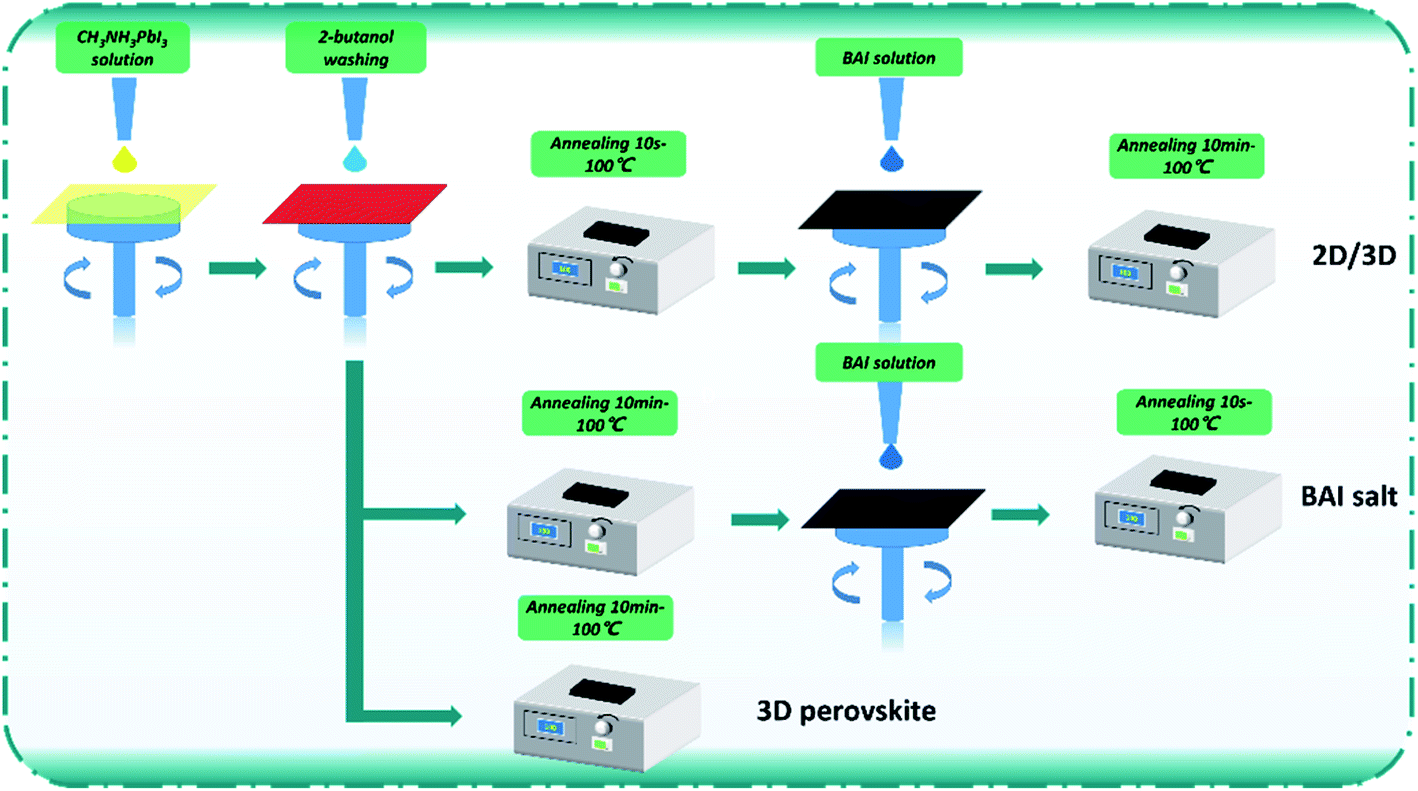 | ||
| Fig. 1 The preparation process of the perovskite films. | ||
After perovskite fabrication, PC61BM (20 mg mL−1 in chlorobenzene) and Bphen (0.7 mg mL−1 in ethanol) were sequentially spin-coated onto the surface of the perovskite film. Finally, a 100 nm thick aluminum (Al) was vacuum evaporated to obtain the cathode.32
2.3 Characterization
Scanning electron microscope (SEM) images and X-ray diffraction (XRD) patterns of the films were obtained with a Zeiss Supra 55 microscope and a Bruker QUANTAX 200 diffractometer, respectively. Atomic force microscopy (AFM) images were obtained using an instrument from Bruker. A sun simulator (Zolix Sirius-SS) was used to provide the simulated solar irradiation (AM 1.5G, 100 mW cm−2). The J–V characteristics were measured using a Keithley 2400 source meter. The output of the light source was adjusted using a calibrated silicon photodiode (ABET technology). The J−V curves were measured by forward scanning from −0.25 to 1.25 V and reverse scanning from 1.25 to −0.25 V. The EQE spectra were measured using a homemade system, in which a light power source (Zolix Sirius-SS), a monochromator (Zolix Omni-λ), and a source meter (Keithley 2400) were used together. The steady-state PL spectra were measured by a fluorescence spectrophotometer (OmniPl-microS, Zolix, China), in which a 600 nm continuous wave laser was passed through the films from the air side.3 Results and discussion
To evaluate the passivation of BAI salts and the resulting formation of two-dimensional perovskite, three kinds of perovskite active layer were fabricated on the HTL surface, the: (1) control sample without a passivation layer, (2) BAI-passivated sample with a thin layer of BAI organic salts on the perovskite surface, and (3) BA2PbI4-passivated sample with a 2D perovskite BA2PbI4 grown on the surface of the CH3NH3PbI3 layer.These three kinds of perovskite films were first evaluated by SEM. The top-view and cross-section SEM images of the control, BAI-passivated, and BA2PbI4-passivated perovskite films are shown in Fig. 2a and b. The control perovskite film exhibited compact, pinhole-free morphology and large perovskite grains were observed which were separated from each other with distinct grain boundaries. The BAI-passivated perovskite film shows a similar morphology as that of the control sample, indicating that a thin covering layer of BAI organic salts is not enough to change the surface texture. In contrast, after the growth of a BA2PbI4 passivation layer on the surface of the CH3NH3PbI3 layer, the exposed surfaces become more homogeneous and smoother, and inconspicuous grain boundaries appear. The grain size distribution of the three kinds of perovskite films was calculated, as shown in Fig. 3. The average grain sizes in the control, BAI-passivated and BA2PbI4 passivated perovskite films are 410 ± 170 nm, 384 ± 160 and 293 ± 139 nm, respectively. The BA2PbI4 passivated sample shows smaller grain sizes than that of control and BAI-passivated samples.33 However, the BA2PbI4 passivated perovskite film is also formed by a single layer of perovskite grains (Fig. 2d–f). Thus, the photon-generated charge carriers can be transported and collected through a single grain without encountering grain boundaries and charge traps, which is the ideal condition for high-performance PSCs.
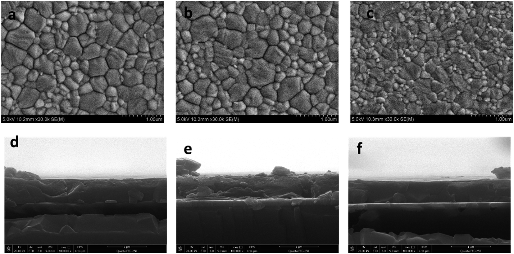 | ||
| Fig. 2 Top-view and cross-section SEM images of the (a and d) control perovskite film, (b and e) BAI-passivated perovskite film, and (c and f) BA2PbI4-passivated perovskite film. The scale bar in the SEM image is 1 μm. | ||
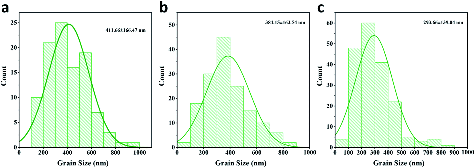 | ||
| Fig. 3 Grain size distribution of the (a) control (b) BAI-passivated and (c) BA2PbI4-passivated perovskite films. | ||
Although the decrease of grain size in the BA2PbI4 passivated sample tends to increase the number of longitudinal grain boundaries, the coverage of the BA2PbI4 passivation layer fills these grain boundaries and reduces the defect concentration induced by grain boundaries. Because BA+ can modify the film morphology, decrease the defect states and enhance the crystallinity for tin perovskites.34–36 To verify this hypothesis, AFM was utilized to observe the surface morphologies of the three kinds of perovskite films and the root mean square roughness (RSM) is used to characterize the height distribution parameters of the surface roughness. Fig. 4 exhibits the AFM images and the height profiles along the surface of perovskite films. The RSM roughness of the control, BAI-passivated, and BA2PbI4-passivated perovskite films were 13.78, 12.63, and 7.39 nm, respectively. A lower value means a flatter sample, the decreased roughness of the BAI-passivated and BA2PbI4-passivated perovskite films indicates that the passivation layer covers the surface of CH3NH3PbI3 films. Furthermore, the height difference between the grain surface and grain boundaries were significantly reduced after the BA2PbI4-passivation. This indicated that BA2PbI4-passivation is more easily achieved at the grain boundaries.14,18,34
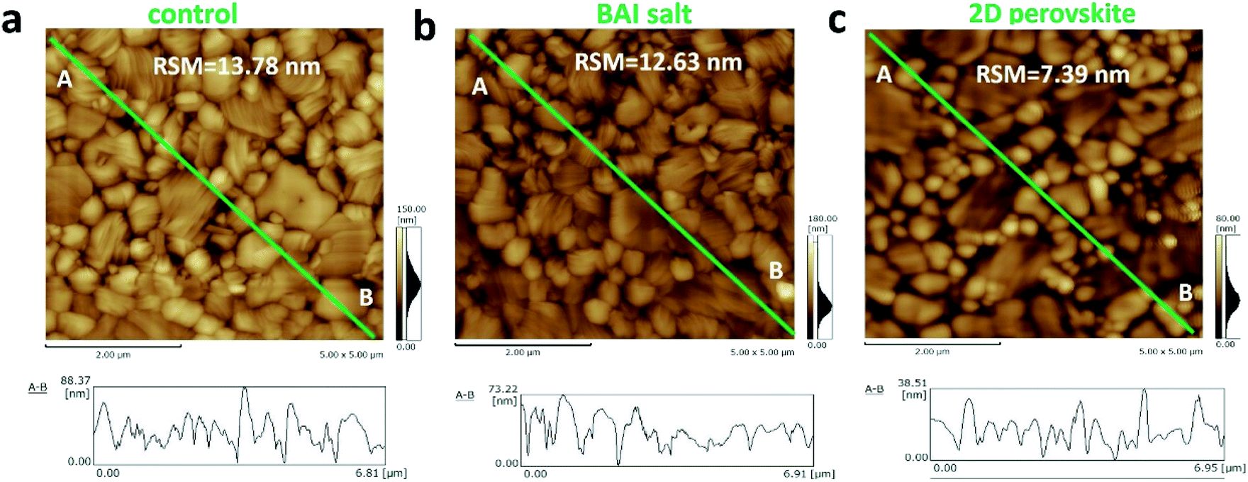 | ||
| Fig. 4 AFM images of the (a) control, (b) BAI-passivated, and (c) BA2PbI4-passivated perovskite films. | ||
To study the crystallinity of the samples after the BAI and BA2PbI4 passivation, the perovskite films were characterized by XRD, as shown in Fig. 5. The control perovskite showed a diffraction peak at 13.1°, which was decreased at the BAI sample and disappeared at the BA2PbI4-passivated sample. This diffraction peak at 13.1° represents the perovskite precursor of PbI2. The XRD patterns indicate that the control perovskite film contained some remnant crystalline PbI2. The BAI coverage layer decreased the PbI2 content on the surface of the film but not inside the film. The PbI2 inside the grains or at the grain boundaries showed incomplete reaction during the BAI treatment, resulting in deep-seated defect states which were not passivated by the surface BAI organic salts. On the other hand, PbI2 was efficiently removed in the presence of the BA2PbI4-passivation layer,37 successfully suppressing defects in the film.38 In addition, as shown in Fig. 5a and b, a new diffraction peak at 6.8° corresponding to the two-dimensional perovskite (BA2PbI4) was observed, which means a BA2PbI4 covering layer was successfully formatted on the surface of the perovskite film.39,40
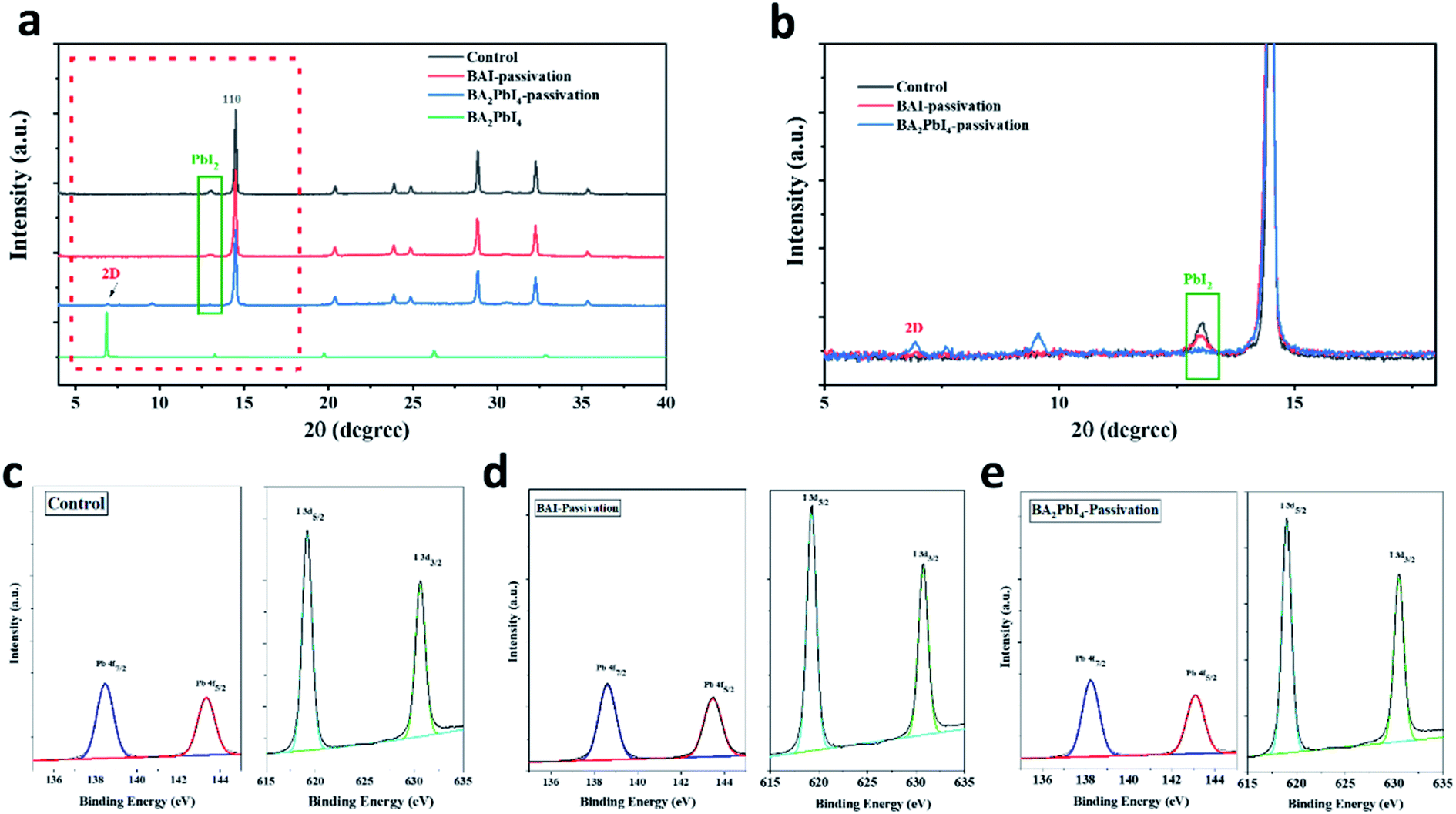 | ||
| Fig. 5 (a) XRD patterns of the control, BAI-passivated, and BA2PbI4-passivated perovskite films. (b) Enlarged view of XRD patterns of the control, BAI-passivated, and BA2PbI4-passivated perovskite films. XPS spectra of (c) control, (d) BAI-passivated (e) BA2PbI4-passivated perovskite films. The Pb 4f and I 3d core-level energy spectra are shown for comparative analysis. | ||
Furthermore, in order to clarify whether BA2PbI4-passivation forms a 2D perovskite BA2PbI4 layer on the perovskite film, we performed XPS element analysis on the perovskite film to study the change of the film element composition. According to the Pb 4f and I 3d core-level energy spectra shown in Fig. 5c–e, it can be estimated that the Pb:I ratio for the control perovskite film is 1:2.79, which indicates that the surface is seriously iodine deficient, which could lead to obvious point defects. After BAI passivation and BA2PbI4 passivation, the Pb:I ratio dramatically increased to 1:3.22 and 1:2.96, indicating the presence of abundant iodide on the perovskite surface and that the iodine vacancy is likely to be filled. Since the XPS test can only detect the element changes on the film surface, and the ratio of peaks after BA2PbI4-passivation is lower than that of BAI-passivation. We believe that this is because BA2PbI4 further filled the perovskite grain boundary and passivated the film defects, resulting in a reduced peak ratio, which is also consistent with the previous AFM roughness test results. Combining the above XRD and XPS analysis, it can be concluded that BA2PbI4 were successfully formed on the surface and grain boundaries of perovskite film.
In order to further explore the effect of the BAI and BA2PbI4 covering layers on the perovskite surface, we measured the UV-Vis and PL spectra of the control, BAI-passivated, and BA2PbI4-passivated perovskite films. As shown in Fig. 6a, the three kinds of films have similar absorption spectra, indicating that the thickness of the BAI and BA2PbI4 layers is thin enough not to affect the perovskite absorption performance.38 Since the three kinds of perovskite film have strong absorption at short wavelengths, a 600 nm excitation light was applied to generate a large density of charge-carriers close to the surface of the perovskite. Fig. 6b shows the PL spectra of the three kinds of perovskite films. The control sample shows a PL peak at 778 nm; this peak showed a 3 nm and 4 nm blueshift after BAI-passivation and BA2PbI4-passivation, respectively. It is well known that the spontaneous radiative recombination induced by trap states usually leads to a redshift compared with the PL emission from the band-edge transition, and hence, passivation of these trap states can blueshift the PL peak.41 The analysis of the PL spectra demonstrated that the BA2PbI4 covering layer could passivate the defects near the surface of the perovskite film more effectively.
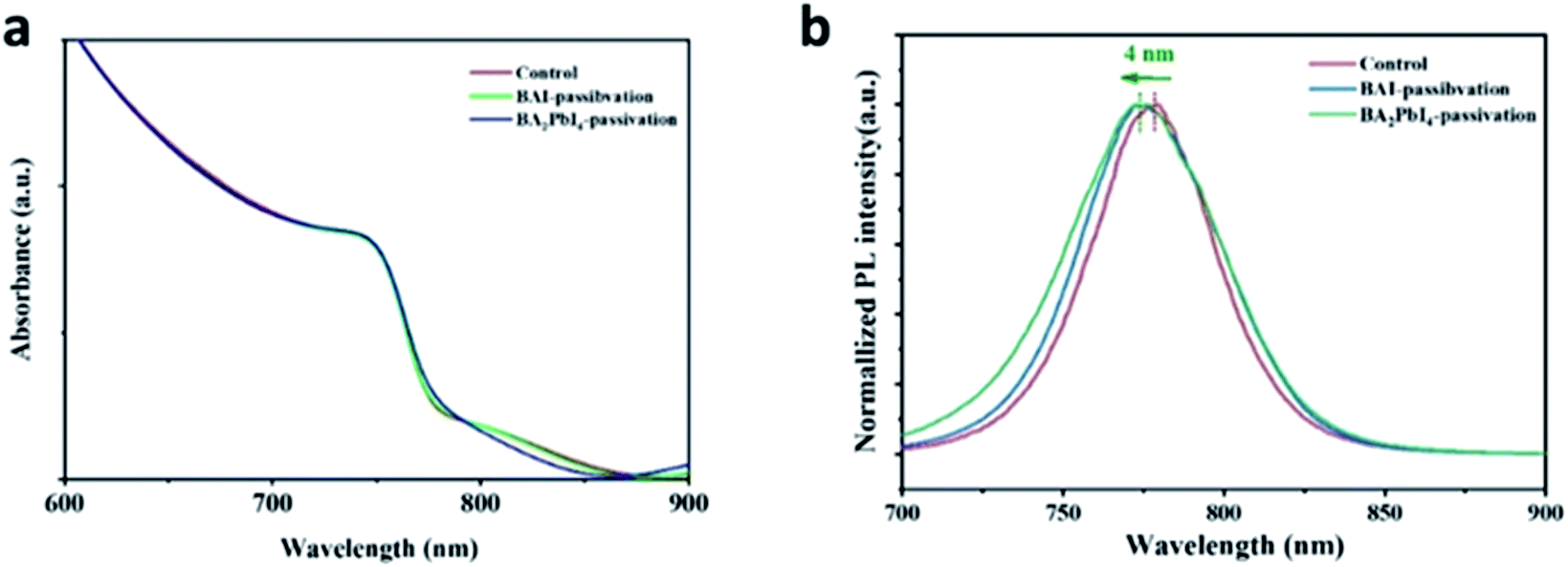 | ||
| Fig. 6 (a) UV-Vis and (b) PL spectra of the control, BAI-passivated, and BA2PbI4-passivated perovskite films. | ||
Besides, fluorescence-lifetime imaging microscopy (FLIM) was measured to uncover the effect of passivation layer on the carrier lifetime of perovskite film. Fig. 7a–c are the FLIM images of the control, BAI-passivated and BA2PbI4-passivated perovskite films. The different colors in the FLIM images represent different PL lifetimes, and the brightness of the images represent the PL intensity. Fig. 7d are the PL lifetimes statistical histogram of the three kinds of perovskite films. Meanwhile, the represents time-resolved PL decay curves for the three kinds of films are shown in Fig. 7e. It can be found that the PL lifetime of the control sample is concentrated around 230 ns, while the PL lifetimes of BAI-passivated and BA2PbI4-passivated samples increase to around 310 and 375 ns, respectively. In addition, Fig. 7d shows that the number of photons in the perovskite film were also increased after BAI and BA2PbI4 passivation treatment. Usually, the trap states in the perovskite film is used as a carrier non-radiative recombination center, resulting in a significant decrease in PL intensity and lifetime. The perovskite film after BA2PbI4-passivation has a longest PL lifetime and the greatest number of PL photons, indicating that the BA2PbI4-passivation treatment has the best passivation ability for film trap states.
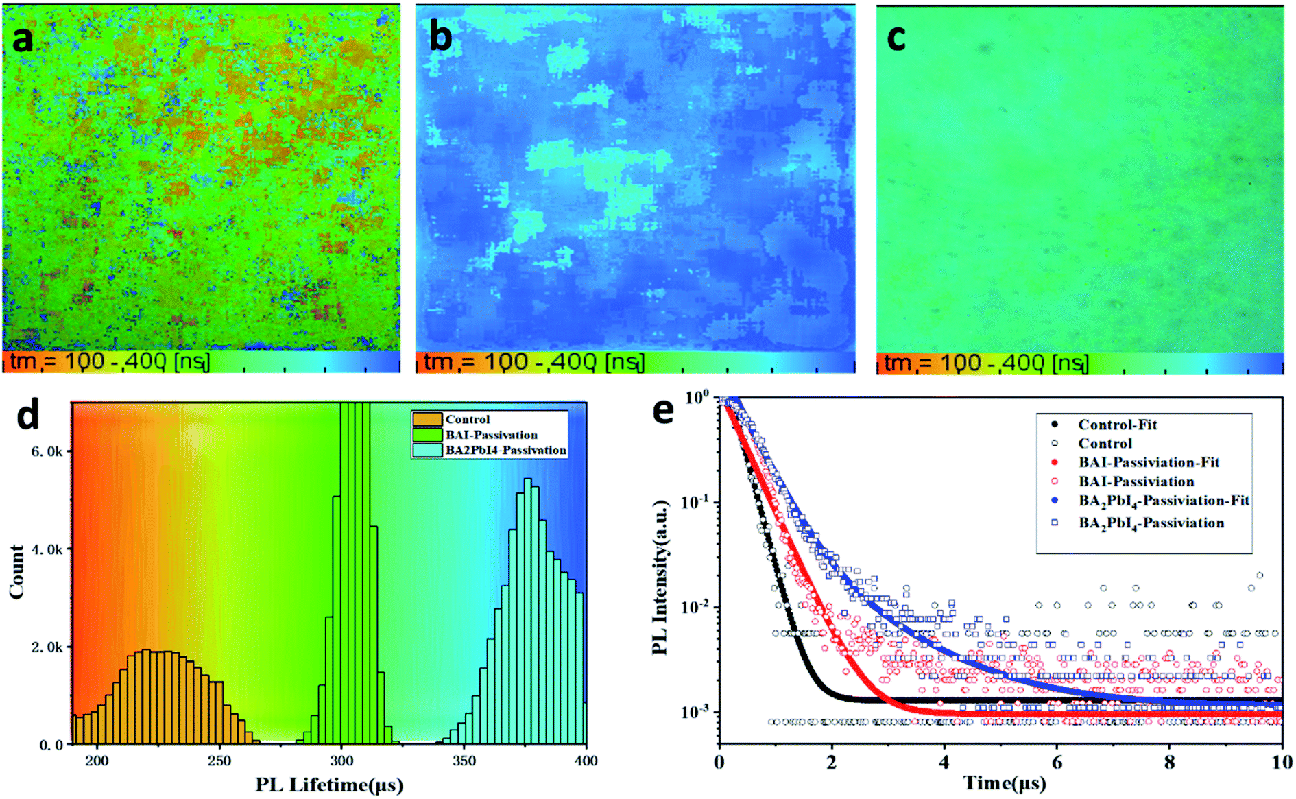 | ||
| Fig. 7 PL lifetime images of (a) control, (b) BA2PbI4-passivation and (c) BAI-passivation treated perovskite films. (d) The representative PL decay curves of the three kinds of perovskite films. | ||
More optoelectronic tests are used to further analyze the influence of the passivation layer on the device performance. Fig. 8a shows the Nyquist plots of the three devices. The measurements are performed in a dark environment with a voltage bias at 0.95 V. The Nyquist plots can be well fitted by the equivalent circuit diagram in the upper part of Fig. 8a to obtain the composite resistance. The control, BAI-passivated and BA2PbI4-passivated devices show the composite resistance of 3.2, 11.5 and 24.4 kΩ, respectively. Besides, it can be seen from Fig. 8b–d that the composite resistance of the BA2PbI4-passivated device shows the highest composite resistance under different bias voltages. These results confirmed that BA2PbI4-passivation treatment exhibits superior suppression effect on the non-radiative recombination induced by the trap states.
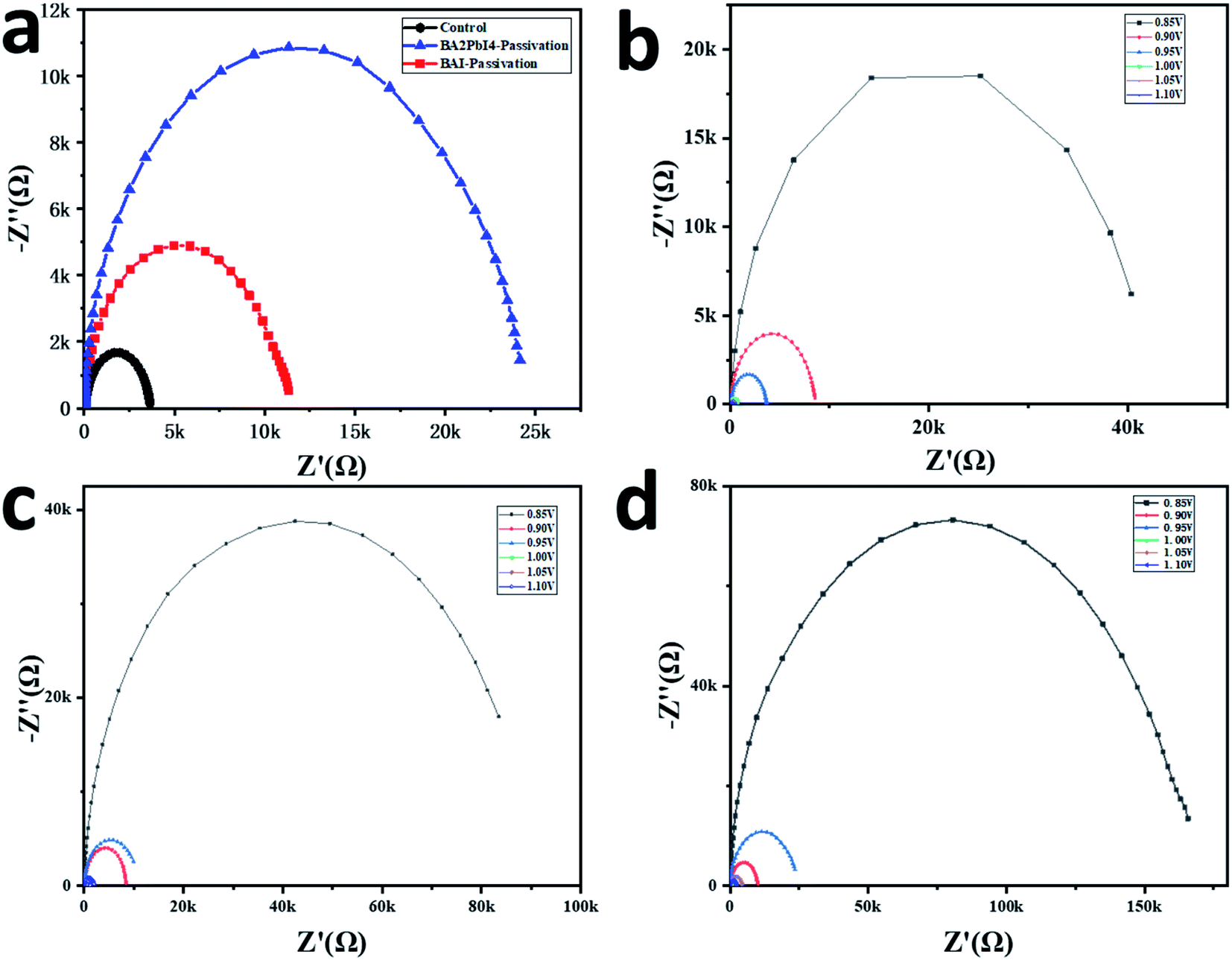 | ||
| Fig. 8 (a) Nyquist plots measured at 0.95 V applied voltage of the control, BAI-passivated, and BA2PbI4-passivated perovskite devices. Nyquist plots measured at different applied voltages for the (b) control (c) BAI-passivated devices and (d) BA2PbI4-passivation. | ||
To further investigate the passivation effect of BAI and BA2PbI4 on the perovskite film, three kinds of PSCs were fabricated with a device structure containing a sandwich with ITO, PTAA: F4-TCNQ, PMMA, the perovskite, PCBM, Bphen, and Al. In this inverted PSC, the PTAA doping with F4-TCNQ was employed as the hole transport layer (HTL); a thin PMMA layer was used as the passivation layer between HTL and the perovskite active layer; three kinds of CH3NH3PbI3 layers were fabricated as the active layers; a PCBM layer modified with Bphen was used as the electron transport layer; and finally, Al was deposited as the cathode. Fig. 9a and b show the device structure and cross-section SEM image of typical BA2PbI4-passivated PSC fabricated in this study, respectively.
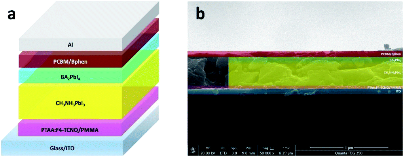 | ||
| Fig. 9 (a) Device structure and (b) cross-sectional SEM image of the BA2PbI4-passivated PSCs. | ||
The J–V curves of the control, BAI-passivated, and BA2PbI4-passivated PSCs showing the best efficiency are shown in Fig. 10. The photovoltaic performance parameters are listed in Table 2. The best-performing control device exhibit a JSC of 23.4 mA cm−2, a VOC of 1.03 V, a FF of 0.74 and a PCE of 17.9% in the forward scan direction. The J–V hysteresis occurs in the control device due to the high density of defects in the perovskite surface. Therefore, the control device displays different photovoltaic performance during the reverse scan direction, with a JSC of 23.3 mA cm−2, a VOC of 1.04 V, an FF of 0.80 and a PCE of 19.3%. The best-performing BAI-passivated device was obtained at a BAI concentration of 0.5 mg mL−1, achieving a JSC of 23.2 mA cm−2, a VOC of 1.07 V, an FF of 0.75 and a PCE of 18.7% in the forward scanning direction and a JSC of 23.0 mA cm−2, a VOC of 1.03 V, a FF of 0.77 and a PCE of 19.00% in the reverse scanning direction. The J–V hysteresis in the BAI-passivated device was significantly inhibited by the surface BAI covering layer.
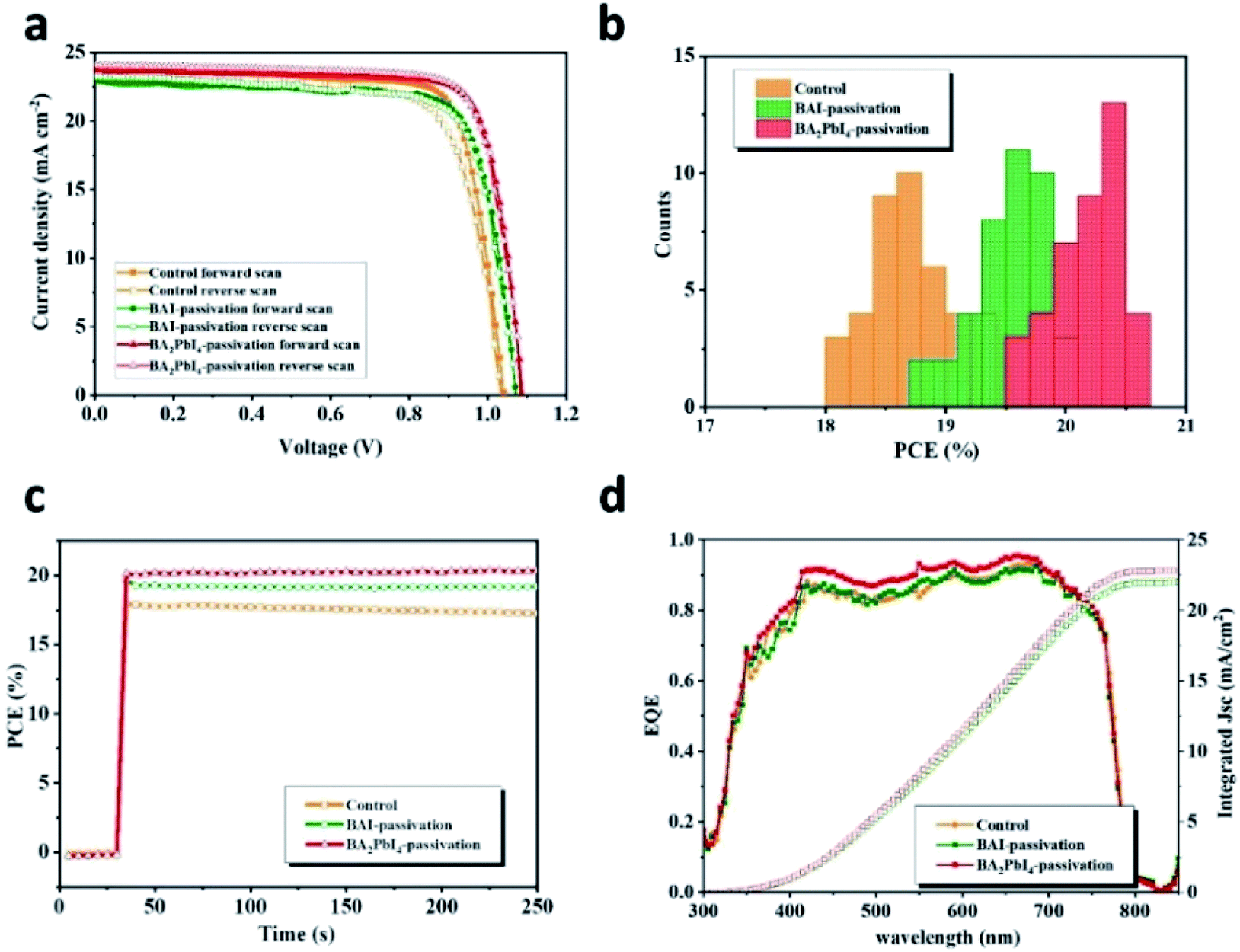 | ||
| Fig. 10 (a) The J–V curves of the best-efficiency control, BAI-passivated, and BA2PbI4-passivated PSCs. (b) Statistics of the PCE distribution from 40 devices of control, BAI-passivated, and BA2PbI4-passivated PSCs. (c) Steady-state power output corresponding to the maximum power point. (d) EQE spectra of best-efficiency control, BAI-passivated, and BA2PbI4-passivated PSCs. | ||
| Device | Scanning direction | VOC (V) | JSC (mA cm−2) | FF (%) | PCE (%) |
|---|---|---|---|---|---|
| Control | Reverse | 1.03 | 23.4 | 0.74 | 17.9 |
| Forward | 1.04 | 23.3 | 0.80 | 19.3 | |
| BAI-Passivated | Reverse | 1.07 | 23.2 | 0.75 | 18.7 |
| Forward | 1.07 | 23.0 | 0.77 | 19.0 | |
| BA2PbI4-Passivated | Reverse | 1.08 | 24.0 | 0.79 | 20.7 |
| Forward | 1.09 | 23.7 | 0.80 | 20.6 |
For the BA2PbI4-passivated PSCs, the concentration of the BAI solution was changed so as to vary the thickness of the BAI induced BA2PbI4-passivation layers. The J–V curves and photovoltaic performance parameters of typical BA2PbI4-passivated PSCs with different BAI concentrations are shown in Fig. 11 and Table 3, respectively. Upon increasing the concentration of BAI from 0, 0.1, 0.2, 0.5, 1 to 5 mg mL−1, the VOC increased to 1.05, 1.07, 1.08, 1.08, 1.09 to 1.10 V, respectively. These results correspond to the increase of defect passivation caused by the increase in the passivation layer thickness. However, to elevate the thickness of the BA2PbI4-passivation layer, the JSC and FF values were gradually increased and reached a maximum value at 0.2 mg mL−1. With the further increase of the thickness of the BA2PbI4-passivation layer, the values of JSC and FF decreased rapidly. This result can be explained by the large thickness of the BA2PbI4-passivation layer, which reduces the electron-extraction ability. We obtained the highest-efficiency BA2PbI4-passivated PSC at a BAI concentration of 0.2 mg mL−1. After optimization, the best-efficiency BA2PbI4-passivated devices achieved a JSC of 24.0 mA cm−2 (23.7 mA cm−2), a VOC of 1.08 V (1.09 V), an FF of 0.79 (0.80) and a PCE of 20.7% (20.6%) in forward (or reverse) scanning direction.
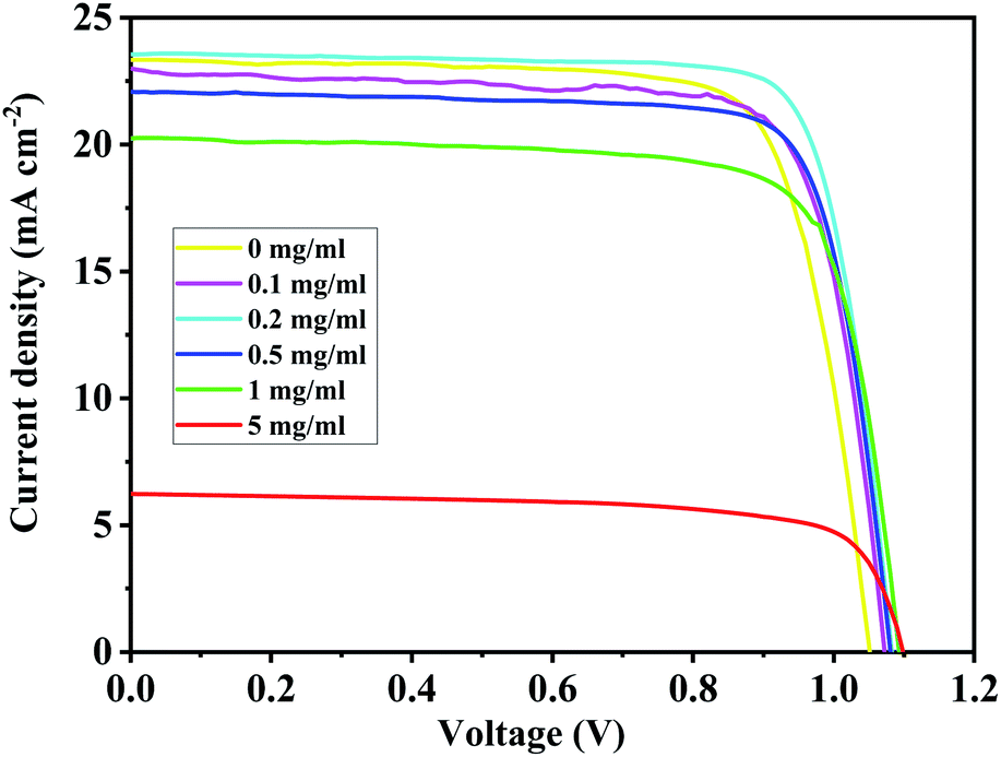 | ||
| Fig. 11 The J–V curves of typical BA2PbI4-passivated PSCs with different BAI concentration. | ||
| BAI (mg mL−1) | VOC (V) | JSC (mA cm−2) | FF (%) | PCE (%) |
|---|---|---|---|---|
| 0 | 1.05 | 23.0 | 0.76 | 18.4 |
| 0.1 | 1.07 | 23.3 | 0.77 | 19.2 |
| 0.2 | 1.08 | 23.6 | 0.80 | 20.4 |
| 0.5 | 1.08 | 23.2 | 0.79 | 19.9 |
| 1 | 1.09 | 20.3 | 0.76 | 16.9 |
| 5 | 1.10 | 6.2 | 0.71 | 4.9 |
In order to visualize the universality of performance improvement, we gathered the PCE distribution from 40 devices of control, BAI-passivated, and BA2PbI4-passivated PSCs. As shown in Fig. 10b, the BA2PbI4-passivated PSCs have the highest average PCE of 20 ± 0.43%; thus, BA2PbI4-passivation is an ideal choice for surface passivation of the PSCs. The best-efficiency BA2PbI4-passivated PSC showed a stabilized PCE of 20.6%, which is consistent with the value from the J–V curve. It is worth noting that in the steady-state test of continuous light for 200 s, the steady-state output power of the control and the BAI-passivation group is lower than that of the BA2PbI4-passivation group. These results suggest that the BA2PbI4-passivation provides better stability for the PSC. The integrated JSC values from the external quantum efficiency (EQE) spectra are 22.1, 22.0 and 22.9 mA cm−2 for the best-efficiency control, BAI-passivated, and BA2PbI4-passivated PSCs, respectively, which agree well with the values from the J–V measurements. Furthermore, the increase in the values of JSC for the BA2PbI4-passivated PSCs can be explained by the suppression of surface charge recombination.
Next, we explore in detail the effect of BAI and BA2PbI4 covering layers on PSCs stability. Fig. 12 shows the time-dependent PCE values of the control, BAI-passivated, and BA2PbI4-passivated PSCs under two different storage conditions, i.e., in a dry cabinet with 5% humidity and under air with 60% humidity. In the high-humidity air environment, the PCE of the three kinds of PSCs dropped to <1% of their initial PCE value within 5 h, but the BA2PbI4-passivated devices showed a little better stability than the others. After storing for 30 days in the drying cabinet, the PCE of the control maintained 53.2% of its initial value, while the PCE value of the BAI-passivated and BA2PbI4-passivated devices remained 65.1% and 72.1% after the same duration. The BA2PbI4-passivated PSC showed better environmental stability. This is due to the stronger van der Waals interaction between the organic molecules and the [PbI6] units in the 2D perovskite materials. Additionally, the organic components of the BA2PbI4 perovskite materials have longer alkyl chains and are more hydrophobic than MA+ ions. In addition, the BA2PbI4-passivation layer may also protect the device from humidity degradation, possibly by reducing the availability of ion trapping sites.15,42,43
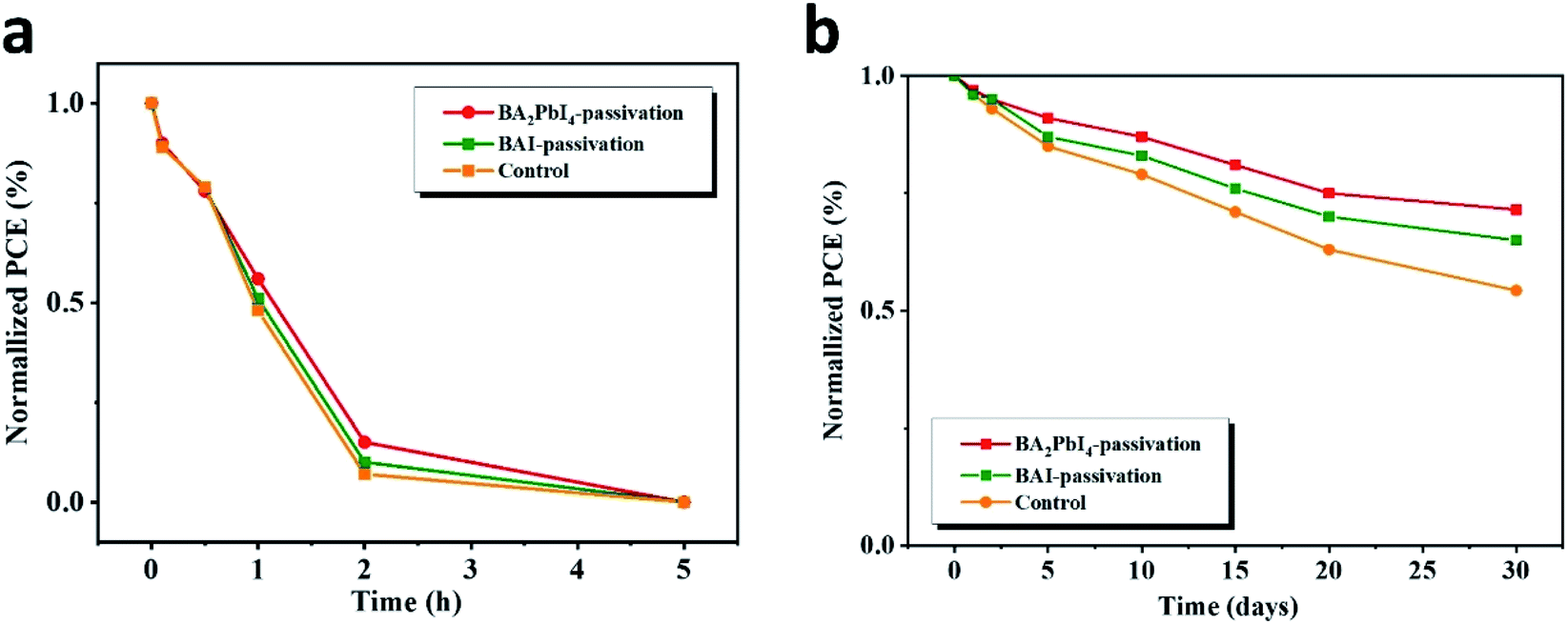 | ||
| Fig. 12 Dark storage stability of the nonencapsulated control, BAI-passivated, and BA2PbI4-passivated samples. The devices were stored in a dark box with humidity of (a) 60% and (b) 5%. | ||
4 Conclusion
In this study, a 2D perovskite BA2PbI4 layer and BAI organic salt itself was formed on the CH3NH3PbI3 surface by optimizing the post-annealing process. A variety of characterization results suggest that the 2D BA2PbI4-passivation layer had a stronger ability to passivate the surface defects of CH3NH3PbI3 films by covering the surface and filling the grain boundaries of active layer. It is also found that the BA2PbI4 passivated perovskite film has longest PL lifetime and highest composite resistance, which further confirmed their superior suppression effect on the non-radiative recombination induced by the trap states. As a consequence, a remarkably enhanced PCE of 20.6% was achieved in the BA2PbI4-passivated inverted PSC. Finally, the BA2PbI4-passivated device has better stability than the control and BAI-passivated devices, and it can still maintain more than 50% of the original device performance after 30 days storage in the drying oven. Our work provides an effective approach to achieve high efficiency and long-term operational stability for the advanced PSC technique.Conflicts of interest
There are no conflicts to declare.Acknowledgements
This work has been partially supported by National Natural Science Foundation of China (61620106016/61835009/61804099/62074108/61775145/61975132); Guangdong Province Key Area R&D Program (2019B110233004).References
- S. D. Stranks, G. E. Eperon, G. Grancini, C. Menelaou, M. J. P. Alcocer, T. Leijtens, L. M. Herz, A. Petrozza and and H. J. Snaith, Science, 2013, 342, 341–344 CrossRef CAS PubMed.
- M. Saliba, T. Matsui, J. Y. Seo, K. Domanski, J. P. Correa-Baena, M. K. Nazeeruddin, S. M. Zakeeruddin, W. Tress, A. Abate, A. Hagfeldt and and M. Gratzel, Energy Environ. Sci., 2016, 9, 1989–1997 RSC.
- G. Delport, S. Macpherson and S. D. Stranks, Adv. Energy Mater., 2020, 10, 13 Search PubMed.
- H. Kim, K.-G. Lim and T.-W. Lee, Energy Environ. Sci., 2016, 9, 12–30 RSC.
- Y. BAI, X. Meng and and S. Yang, Adv. Energy Mater., 2018, 8, 1701883 CrossRef.
- Z. P. Wang, Q. Q. Lin, B. Wenger, M. G. Christoforo, Y. H. Lin, M. T. Klug, M. B. Johnston, L. M. Herz and H. J. Snaith, Nat. Energy, 2018, 3, 1013 CrossRef.
- W. Zhao, J. Shi, C. Tian, J. Wu, H. Li, Y. Li, B. Yu, Y. Luo, H. Wu, Z. Xie, C. Wang, D. Duan, D. Li and Q. Meng, ACS Appl. Mater. Interfaces, 2021, 13, 9771–9780 CrossRef CAS PubMed.
- S. Feldmann, S. Macpherson, S. P. Senanayak, M. Abdi-Jalebi, J. P. H. Rivett, G. J. Nan, G. D. Tainter, T. A. S. Doherty, K. Frohna, E. Ringe, R. H. Friend, H. Sirringhaus, M. Saliba, D. Beljonne, S. D. Stranks and F. Deschler, Nat. Photonics, 2020, 14, 123 CrossRef CAS.
- W. Chen, Y. Z. Wu, Y. F. Yue, J. Liu, W. J. Zhang, X. D. Yang, H. Chen, E. B. Bi, I. Ashraful, M. Gratzel and L. Y. Han, Science, 2015, 350, 944–948 CrossRef CAS PubMed.
- W. S. Yang, B.-W. Park, E. H. Jung, N. J. Jeon, Y. C. Kim, D. U. Lee, S. S. Shin, J. Seo, E. K. Kim, J. H. Noh and S. I. Seok, Science, 2017, 356, 1376 CrossRef CAS PubMed.
- M. Saliba, T. Matsui, K. Domanski, J. Y. Seo, A. Ummadisingu, S. M. Zakeeruddin, J. P. Correa-Baena, W. R. Tress, A. Abate, A. Hagfeldt and M. Gratzel, Science, 2016, 354, 206–209 CrossRef CAS PubMed.
- A. Fakharuddin, L. Schmidt-Mende, G. Garcia-Belmonte, R. Jose and I. Mora-Sero, Adv. Energy Mater., 2017, 7, 1700623 CrossRef.
- M. Abdi-Jalebi, Z. Andaji-Garmaroudi, S. Cacovich, C. Stavrakas, B. Philippe, J. M. Richter, M. Alsari, E. P. Booker, E. M. Hutter, A. J. Pearson, S. Lilliu, T. J. Savenije, H. Rensmo, G. Divitini, C. Ducati, R. H. Friend and S. D. Stranks, Nature, 2018, 555, 497 CrossRef CAS PubMed.
- X. Li, D. Q. Bi, C. Y. Yi, J. D. Decoppet, J. S. Luo, S. M. Zakeeruddin, A. Hagfeldt and M. Gratzel, Science, 2016, 353, 58–62 CrossRef CAS PubMed.
- G. Grancini, C. Roldan-Carmona, I. Zimmermann, E. Mosconi, X. Lee, D. Martineau, S. Narbey, F. Oswald, F. De Angelis, M. Graetzel and M. K. Nazeeruddin, Nat. Commun., 2017, 8, 15684 CrossRef CAS PubMed.
- H. R. Tan, A. Jain, O. Voznyy, X. Z. Lan, F. P. G. de Arquer, J. Z. Fan, R. Quintero-Bermudez, M. J. Yuan, B. Zhang, Y. C. Zhao, F. J. Fan, P. C. Li, L. N. Quan, Y. B. Zhao, Z. H. Lu, Z. Y. Yang, S. Hoogland and E. H. Sargent, Science, 2017, 355, 722–726 CrossRef CAS PubMed.
- X. Meng, C. H. Y. Ho, S. Xiao, Y. BAI, T. Zhang, C. Hu, H. Lin, Y. Yang, S. K. So and S. Yang, Nano Energy, 2018, 52, 300–306 CrossRef CAS.
- F. Zhang, J. Song, R. Hu, Y. R. Xiang, J. J. He, Y. Y. Hao, J. R. Lian, B. Zhang, P. J. Zeng and J. L. Qu, Small, 2018, 14, 1704007 CrossRef PubMed.
- L. Zuo, Q. Chen, N. De Marco, Y. T. Hsieh, H. Chen, P. Sun, S. Y. Chang, H. Zhao, S. Dong and Y. Yang, Nano Lett., 2017, 17, 269–275 CrossRef CAS PubMed.
- Q. Jiang, Y. Zhao, X. W. Zhang, X. L. Yang, Y. Chen, Z. M. Chu, Q. F. Ye, X. X. Li, Z. G. Yin and J. B. You, Nat. Photonics, 2019, 13, 460 CrossRef CAS.
- G. Niu, W. Li, J. Li and L. Wang, Sci. China Mater., 2016, 59, 728–742 CrossRef CAS.
- T. S. Sherkar, C. Momblona, L. Gil-Escrig, J. Avila, M. Sessolo, H. J. Bolink and L. J. A. Koster, ACS Energy Lett., 2017, 2, 1214–1222 CrossRef CAS PubMed.
- P. Da and G. Zheng, Nano Res., 2017, 10, 1471–1497 CrossRef CAS.
- K. Yoshikawa, H. Kawasaki, W. Yoshida, T. Irie, K. Konishi, K. Nakano, T. Uto, D. Adachi, M. Kanematsu, H. Uzu and K. Yamamoto, Nat. Energy, 2017, 2, 8 Search PubMed.
- S. Singh, L. Laxmi and D. Kabra, J. Phys. D: Appl. Phys., 2020, 53, 24 Search PubMed.
- I. C. Smith, E. T. Hoke, D. Solis-Ibarra, M. D. McGehee and H. I. Karunadasa, Angew. Chem., Int. Ed., 2014, 53, 11232–11235 CrossRef CAS PubMed.
- J.-P. Correa-Baena, W. Tress, K. Domanski, E. H. Anaraki, S.-H. Turren-Cruz, B. Roose, P. P. Boix, M. Grätzel, M. Saliba, A. Abate and A. Hagfeldt, Energy Environ. Sci., 2017, 10, 1207–1212 RSC.
- M. Kim, S. G. Motti, R. Sorrentino and A. Petrozza, Energy Environ. Sci., 2018, 11, 2609–2619 RSC.
- J. Chen, D. Lee and N. G. Park, ACS Appl. Mater. Interfaces, 2017, 9, 36338–36349 CrossRef CAS PubMed.
- Y. Lin, Y. BAI, Y. J. Fang, Z. L. Chen, S. Yang, X. P. Zheng, S. Tang, Y. Liu, J. J. Zhao and J. S. Huang, J. Phys. Chem. Lett., 2018, 9, 654–658 CrossRef CAS PubMed.
- F. Zhang, J. J. He, Y. R. Xiang, K. Zheng, B. Xue, S. Ye, X. Peng, Y. Y. Hao, J. R. Lian, P. J. Zeng, J. L. Qu and J. Song, Adv. Mater., 2018, 30, 1803244 CrossRef PubMed.
- F. Zhang, J. Song, L. X. Zhang, F. F. Niu, Y. Y. Hao, P. J. Zeng, H. B. Niu, J. S. Huang and J. R. Lian, J. Mater. Chem. A, 2016, 4, 8554–8561 RSC.
- W. Q. Wu, Z. B. Yang, P. N. Rudd, Y. C. Shao, X. Z. Dai, H. T. Wei, J. J. Zhao, Y. J. Fang, Q. Wang, Y. Liu, Y. H. Deng, X. Xiao, Y. X. Feng and J. S. Huang, Sci. Adv., 2019, 5, 8925 CrossRef PubMed.
- E. Jokar, C. H. Chien, A. Fathi, M. Rameez, Y. H. Chang and W. G. Diau, Energy Environ. Sci., 2018, 11, 2353–2362 RSC.
- F. Zhang, Q. Huang, J. Song, Y. Zhang, C. Ding, F. Liu, D. Liu, X. Li, H. Yasuda, K. Yoshida, J. Qu, S. Hayase, T. Toyoda, T. Minemoto and Q. Shen, Sol. RRL, 2020, 4, 1900243 CrossRef CAS.
- X. P. Zheng, B. Chen, J. Dai, Y. J. Fang, Y. Bai, Y. Lin, W. Haotong, X. C. Zeng and J. S. Huang, Nat. Energy, 2017, 2, 17102 CrossRef CAS.
- P. Chen, Y. BAI, S. C. Wang, M. Q. Lyu, J. H. Yun and L. Z. Wang, Adv. Funct. Mater., 2018, 28, 1870113 CrossRef.
- F. Zhang, J. Song, L. X. Zhang, F. F. Niu, Y. Y. Hao, P. J. Zeng, H. B. Niu, J. S. Huang and J. R. Lian, J. Mater. Chem. A, 2016, 4, 8554–8561 RSC.
- M. Abdi-Jalebi, Z. Andaji-Garmaroudi, S. Cacovich, C. Stavrakas, B. Philippe, J. M. Richter, M. Alsari, E. P. Booker, E. M. Hutter, A. J. Pearson, S. Lilliu, T. J. Savenije, H. Rensmo, G. Divitini, C. Ducati, R. H. Friend and S. D. Stranks, Nature, 2018, 555, 497 CrossRef CAS PubMed.
- A. Abate, M. Saliba, D. J. Hollman, S. D. Stranks, K. Wojciechowski, R. Avolio, G. Grancini, A. Petrozza and H. J. Snaith, Nano Lett., 2014, 14, 3247–3254 CrossRef CAS PubMed.
- S. Yang, J. Dai, Z. H. Yu, Y. C. Shao, Y. Zhou, X. Xiao, X. C. Zeng and J. S. Huang, J. Am. Chem. Soc., 2019, 141, 5781–5787 CrossRef CAS PubMed.
- J. Peng, Y. Wu, W. Ye, D. A. Jacobs, H. Shen, X. Fu, Y. Wan, T. Duong, N. Wu, C. Barugkin, H. T. Nguyen, D. Zhong, J. Li, T. Lu, Y. Liu, M. N. Lockrey, K. J. Weber, K. R. Catchpole and T. P. White, Energy Environ. Sci., 2017, 10, 1792–1800 RSC.
- F. Huang, L. Jiang, A. R. Pascoe, Y. Yan, U. Bach, L. Spiccia and Y.-B. Cheng, Nano Energy, 2016, 27, 509–514 CrossRef CAS.
Footnote |
| † Joint first authors. |
| This journal is © The Royal Society of Chemistry 2021 |