
 Open Access Article
 This Open Access Article is licensed under a
 Creative Commons Attribution 3.0 Unported Licence
Stress-induced phase-alteration in solution processed indium selenide thin films during annealing†
Bipanko Kumar Mondal a,
Shaikh Khaled Mostaquea,
Md. Ariful Islamb and
Jaker Hossain*a
a,
Shaikh Khaled Mostaquea,
Md. Ariful Islamb and
Jaker Hossain*a
aSolar Energy Laboratory, Department of Electrical and Electronic Engineering, University of Rajshahi, Rajshahi 6205, Bangladesh. E-mail: jak_apee@ru.ac.bd
bDepartment of Physics, Rajshahi University of Engineering and Technology, Rajshahi 6204, Bangladesh
First published on 13th April 2021
Abstract
This article demonstrates the successful synthesis of indium selenide thin films by a spin coating method in air using thiol-amine cosolvents. The synthesized films encountered a transformation from β-In3Se2 to γ-In2Se3 phase due to mechanical stress during annealing as confirmed from XRD and EDS analysis. The SEM study ensured the homogeneity and uniformity of surface morphology of both phases. The FTIR analysis also confirmed the In–Se stretching vibration bond for both β-In3Se2 and γ-In2Se3 thin films. The temperature dependent electrical conductivity indicated the semiconducting nature of both phases. The optical transmittance was found to increase with annealing temperatures for both phases. The optical band gaps were estimated to be in the range of 2.60–2.75 and 2.12–2.28 eV for β-In3Se2 and γ-In2Se3 phases, respectively consistent with the reported values. These results indicate that stress-induced phase transformation in solution-processed indium selenide could be useful in 2D optoelectronic devices in future.
1. Introduction
Recently, indium selenide (InSe) has been extensively studied because of its high photo-response, tunable band-gap, phase-transition phenomena and excellent electrical transport properties which have made it available in varieties of potential applications. These unique properties make it a suitable candidate for applications in phase-change memories devices and solar energy conversion.1–3 Indium selenide (InSe) belongs to the group of III–VI metal chalcogenide materials. The phase diagram of InSe shows that there are various stable phases with many stoichiometries such as InSe, In2Se, In2Se3, In3Se2, In5Se6, In4Se3, In6Se7, In3Se4 and In2.5Se4 as revealed by many researchers.4–9 Among all of the phases, In2Se3 belongs to α, β, γ, δ, and κ crystalline phases as trivalent and divalent atoms can be amalgamated to fulfill their bonding in the same stoichiometric ratio under different temperatures.10 As a phase change materials, In2Se3 is more fascinated compared to others (for example GeTe, Ge2Sb2Te5 alloy) materials due to renewed optical and electronic properties with the application in multilevel based memories, optoelectronic detectors, sensors and two dimensional (2D) based nano devices.11,12The formation of the In2Se3 phase is difficult to prepare because it is stable at generally under high pressure and temperature. The phase transformation of β-InSe to γ-In2Se3 have been also happened above at 200 °C in thermal annealing process.12 In our previous study, we have also reported phase transition from In2Se3 to highly degenerate In3Se4 phase due to heat treatment.4,13 Apart from the temperature, pressure induced phase transition in In2Se3 phase has also been studied and reported recently.14
The different phases of indium selenide thin films have already been synthesized using various deposition methods, for example Hydrothermal,10 E-beam evaporation,15 Sol–gel,16 Spray pyrolysis,17 Chemical Vapor Deposition (CVD),18 Flash evaporation,19 Molecular Beam Epitaxy (MBE),20 Van der wall epitaxy,21 Thermal evaporation,22 Electro deposition23 Laser irradiation24 etc. However, among all of the deposition methods, solution processed spin coating is the cheapest and easiest method to deposit uniform thin films which, to the best of our knowledge, is not employed yet to deposit indium selenide thin films. It is already reported that a simple thiol-amine solvent system has the ability to dissolve bulk V2VI3 (V = As, Bi, Sb; VI = Te, Se, S) semiconductors and chalcogenide materials.25,26 The solubility of In2Se3 within thiol-amine co-solvents is also reported.27 However, there is no report of fabrication and characterization of indium selenide thin films by this process.
In this article, we demonstrate the synthesis of InSe thin films in air by spin coating method using ethylene-di-amine and 1,2 ethanedi-thiol co-solvents at various annealing temperatures. We also studied the effect of applying mechanical-stress in the indium selenide thin films during annealing.
2. Experimental details
2.1 Preparation of solution
To prepare indium selenide solution, InSe granular powder with 99.999% purity was purchased from Metron, USA and co-solvents ethylene-di-amine and 1,2 ethanedi-thiol were purchased from Sigma Aldrich. The preparation steps of indium selenide solution was represented in Fig. 1a. First, 1 wt% InSe powder was dissolved in the diluted co-solvents ethylene-di-amine and 1,2 ethanedi-thiol at a volume ratio 9![[thin space (1/6-em)]](https://www.rsc.org/images/entities/char_2009.gif) :1. To completely liquefy InSe powder, this solution was stirred using magnetic stirrer at a speed of 350 rpm at 50 °C temperature for 5 hours. After completely dissolving the InSe powder, the solution was light brown in color. Then the solution was filtered using 0.45 μm pore sized syringe filter to remove any additional contaminants from solution.
:1. To completely liquefy InSe powder, this solution was stirred using magnetic stirrer at a speed of 350 rpm at 50 °C temperature for 5 hours. After completely dissolving the InSe powder, the solution was light brown in color. Then the solution was filtered using 0.45 μm pore sized syringe filter to remove any additional contaminants from solution.
 | ||
| Fig. 1 (a) The preparation steps of 1 wt% indium selenide precursor solution and (b) schematic presentation of substrate cleaning and film deposition steps. | ||
2.2 Deposition of indium selenide thin films
Glass substrates (2 × 2 cm2) were used to fabricate indium selenide thin films utilizing thiol-amine cosolvents solution. First, the substrates were cleaned utilizing piranha solution to eliminate gross contaminations and then they were washed by distilled water twice for removing any additional contaminations. After that prepared solution was spin coated on cleaned glass substrate only one time at a speed of 1000 rpm for 30 seconds with a 10 seconds slope at 500 rpm. Then, the deposited indium selenide films were pre-annealed on a hot plate at 100 °C for 10 minutes to dispel residual solvents. After that these pre-annealed films were post-annealed in two different ways for further crystallization of the films. In a first recipe, these films were annealed at 250, 300 and 350 °C temperatures for 10 minutes in a carbolite oven in air without applying any stress. In a second recipe, these film were annealed in the same condition with applying a simple mechanical stress. The mechanical stress was applied on indium selenide thin films using a microscopic glass of 1–1.2 mm thick during annealing. The films were sandwiched between two microscopic glasses which were bound with stainless steel clip on each edges of the glass substrate. The schematic of the substrate cleaning, deposition steps of indium selenide thin films are shown in Fig. 1b.2.3 Characterization of indium selenide thin films
The thickness of the synthesized indium selenide thin films annealed at different temperatures were measured using Bruker Dektak XTL thickness profiler. The structural analysis of the synthesized films were performed by X-ray Diffractometer of model Bruker D8 Advance using monochromatic CuKα radiation (wavelength, λ = 1.5418 Å) in the range of 2θ = 20–80°. The Scanning Electron Microscope (SEM) of model ZEISS EVO-18 was used to visual analysis of surface topology of InSe films. The elemental composition of indium selenide thin films unrolled with an energy dispersive X-ray spectroscopy (EDS) detector attached with SEM. To understand chemical identification of synthesized indium selenide films FTIR spectra in the wavenumber range of 400–4000 cm−1 were also recorded. The FTIR spectra were monitored with a Shimadzu spectrometer (IRTracer-100). A T-60 ultraviolet-visible (UV-vis) Spectrophotometer (PG Instruments) was used to characterize optical properties by studying transmission spectra of indium selenide films.3. Results and discussion
3.1 Annealing and stress effects on indium selenide thin films
Although annealing of films synthesized using thiol-amine cosolvents are performed in inert environment for avoiding oxidation, the synthesized indium selenide thin films were annealed in air. It was observed that annealing in air did not oxidize the films. The thickness of the synthesized films in both the unstressed and stressed cases was found to decrease with annealing temperature. The average thicknesses were ∼370, ∼360 and ∼330 nm for 250, 300 and 350 °C, respectively. However, the decrease in film thickness with the annealing temperature might occur due to the transformation of the film into more ordered phase with reduce defects that causes dimensional shrinkage resulting in the decrease of the film thickness.However, in a previous synthesis of CdS thin films through thiol-amine cosolvent route, a glass protector was used during annealing to suppress oxidation.28 The similar technique that provide simple stress on the films was utilized to visualize its effect on the films. Fig. 2a shows the optical images of indium selenide thin films deposited with and without stress using thiol-amine cosolvents. It is observed from figure that the films have turned into dark brown color from light brown due to the application of stress. This might be resulted from the phase alteration in indium selenide thin films from β-In3Se2 to γ-In2Se3 phase due to stress during annealing. The schematic of phase alteration of β-In3Se2 to γ-In2Se3 phase with their crystal structures are visualized in Fig. 2b. The β-In3Se2 phase has poly-hexagonal crystal structure with space group P63/mmc and γ-In2Se3 crystal also has hexagonal structure with space group P61 including distorted wurtzite-type atomic layout.
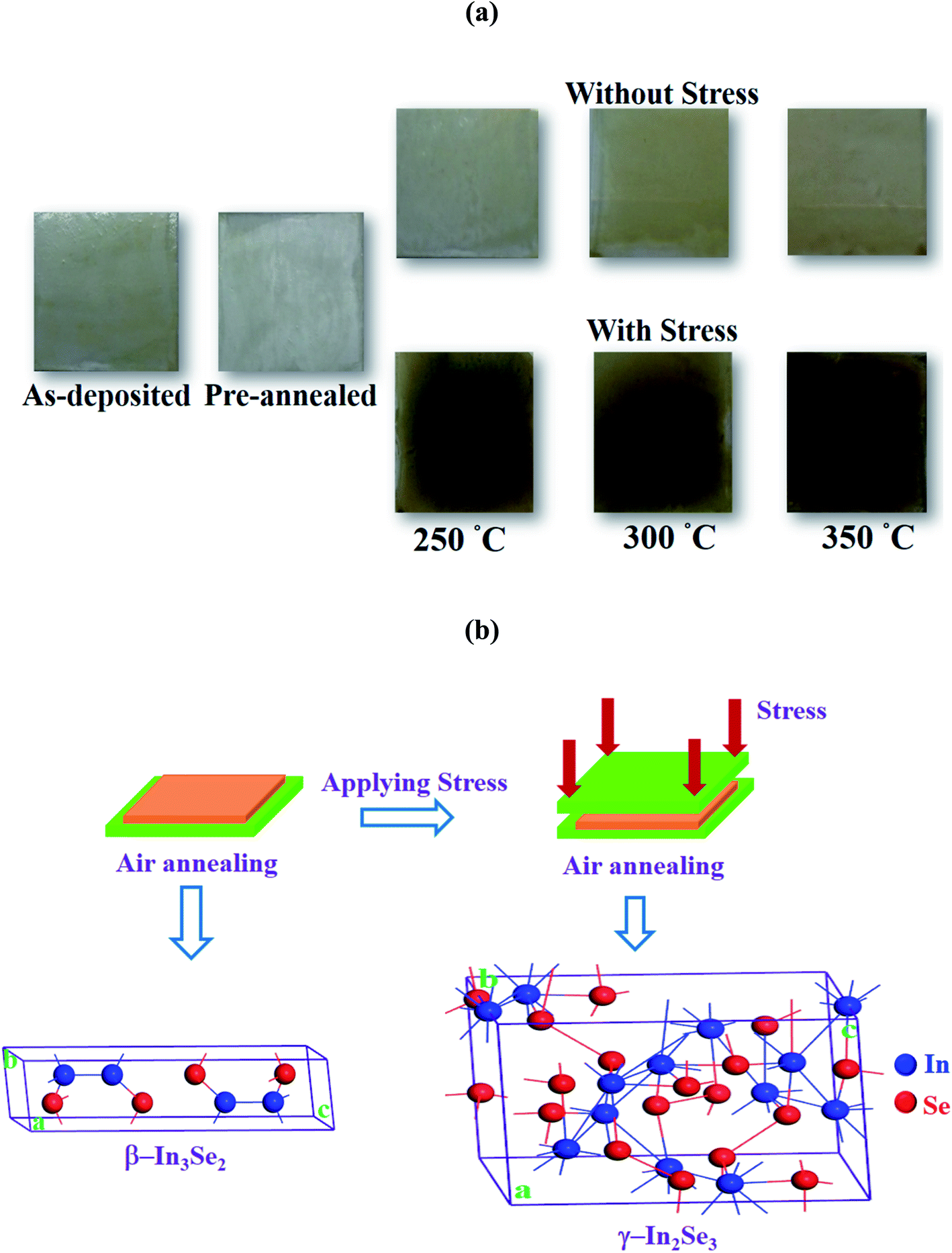 | ||
| Fig. 2 (a) The optical images of synthesized InSe thin films utilizing thiol-amine cosolvents at different annealing temperatures for without and with mechanical stress. (b) Schematic presentation of phase transformation of indium selenide thin films during annealing. | ||
3.2 Structural analysis of indium selenide thin films
 | ||
| Fig. 3 XRD spectra of indium selenide thin films for (a) In3Se2 and (b) In2Se3 phases, respectively deposited by spin coating method using thiol-amine cosolvents. | ||
However, the phase is changed when a simple mechanical stress is applied on the films during annealing which is visualized in Fig. 3b. It is interesting to note that, there is no peak for the films annealed at 250 °C which indicates the amorphous nature of indium selenide thin films. The indium selenide thin films exhibited the same polycrystalline nature at annealing temperatures of 300 and 350 °C. For the films annealed at 300 °C, peaks were originated at around the angle 2θ = 23.16, 25.41, 26.42, 28.8, 31.26 and 52.6° which can be indexed as (104), (111), (112), (200), (106) and (306) planes, respectively. On the other hand, the films annealed at 350 °C exhibited five peaks which were also originated at around the angle 2θ = 26.54, 28.45, 31.95, 52.45 and 55.48° that can be indexed as (112), (113), (203), (306) and (313) planes, respectively according to JCPDS card no. 89-0658. This result indicates the presence of hexagonal structured γ-In2Se3 phase with lattice parameters a = b= 7.12 and c = 19.22 Å.10,12,31 It is also observed that with the presence of stress, the diffraction peaks become sharper with the increase of annealing temperature, suggesting a better crystallinity of γ-In2Se3 sample at 350 °C. It already is reported that γ-In2Se3 phase can be formed at a higher annealing temperature of 600 °C.16 However, in this study γ-In2Se3 phase in indium selenide films was formed at a low temperature of 300 °C and above which is mainly due to the application of mechanical stress. Hence, it can be concluded that solution-processed indium selenide thin films encounter the phase transformation from β-In3Se2 to γ-In2Se3 phase due to the application of mechanical stress during annealing in air.
However, it is also noticed from the figures that the crystallinity of the films in both the phases are relatively poor which could be improved with annealing at higher temperature. But, in this study, the high temperature annealing was not performed as this could result serious oxidation of the films as annealing was performed in open air.28 However, it is also true that very small amount of oxidation might be presented in amorphous form in the synthesized films.
The crystallite size D, full width half maximum (FWHM) β, the dislocation density δ were calculated from the XRD data to know crystallographic information. The crystallite size D, has been calculated using Debye–Scherrer's equation28
 | (1) |
The dislocation density, δ has also been estimated by using the formula32
| δ = 1/D2 | (2) |
Table S1 in the ESI† shows the crystallographic parameters of β-In3Se2 and γ-In2Se3 phase of indium selenide thin films deposited by simple spin coating method using thiol-amine co-solvents. It can be seen from the table that the crystallite size of the β-In3Se2 phase varies in the range of 26–84 nm with dislocation density in the range of (1.4–14.5) × 1014 line per m2. Whereas the crystallite size of the γ-In2Se3 phase varies in the range of 24–56 nm with dislocation density in the range of (3.1–16.4) × 1014 line per m2. It is also observed that crystallite size decreases and dislocation density increases for the films annealed with stress. This lowering of the crystallite size and increase in dislocation density of the In2Se3 thin films due to the application of mechanical stress might be attributed to several factors such as differential stress, strain variation and grain size reduction, and the separation of the effect of each factor is difficult.33
 | ||
| Fig. 4 The SEM images of different magnifications of (a–c) In3Se2 and (d–f) In2Se3 phases, respectively of indium selenide thin films deposited by spin coating method using thiol-amine cosolvents. | ||
:2 for the films annealed without stress at temperatures of 250, 300 and 350 °C, respectively. This indicate the stoichiometric In3Se2 phase which is consistent with the reported work.29 However, the starting materials for the solution was InSe with 1:1 ratio which ended up with 3:2 ratio of In and Se in In3Se2 thin films. This may be happened due to the re-evaporation of Se during annealing which agreed well with the other reports.4,34 On the other hand, In and Se ratio is nearly 2:3 for the films annealed with stress at annealing temperatures of 250, 300 and 350 °C, respectively which ensures the stoichiometric In2Se3 phase of the films.35,36 Here, the thin films are synthesized with 2:3 ratio of In and Se, respectively. This may be happened due to the re-arrangement of In and Se atoms and/or re-evaporation of In during annealing and this result is also consistent with the reported works.12,37 For the both cases, it is also observed from table that the stoichiometric ratio increases with increasing annealing temperatures. The EDS mapping for γ-In2Se3 phase is also shown Fig. S2 in ESI,† which also indicates the increase of In and decrease of Se with increasing annealing temperatures. In the EDS spectra, another component Si (not shown) was detected which was mainly originated from the glass substrate. Other few components such as Na, Mg, O, N, Pt, Ca, S and C were detected in negligibly small amount that were also ignored in EDS spectra. Therefore, the phase transformation from In3Se2 to In2Se3 phase due to stress during annealing can also be assured from EDS study.
| Annealing temperature (°C) | In3Se2 phase | In2Se3 phase | ||||
|---|---|---|---|---|---|---|
| Elements | Stoichiometric ratio In/Se | Elements | Stoichiometric ratio In/Se | |||
| In (at%) | Se (at%) | In (at%) | Se (at%) | |||
| 250 | 56.92 | 43.08 | 1.32 | 37.25 | 62.75 | 0.594 |
| 300 | 61.03 | 38.97 | 1.57 | 40.10 | 59.90 | 0.669 |
| 350 | 62.32 | 37.68 | 1.65 | 41.40 | 58.60 | 0.706 |
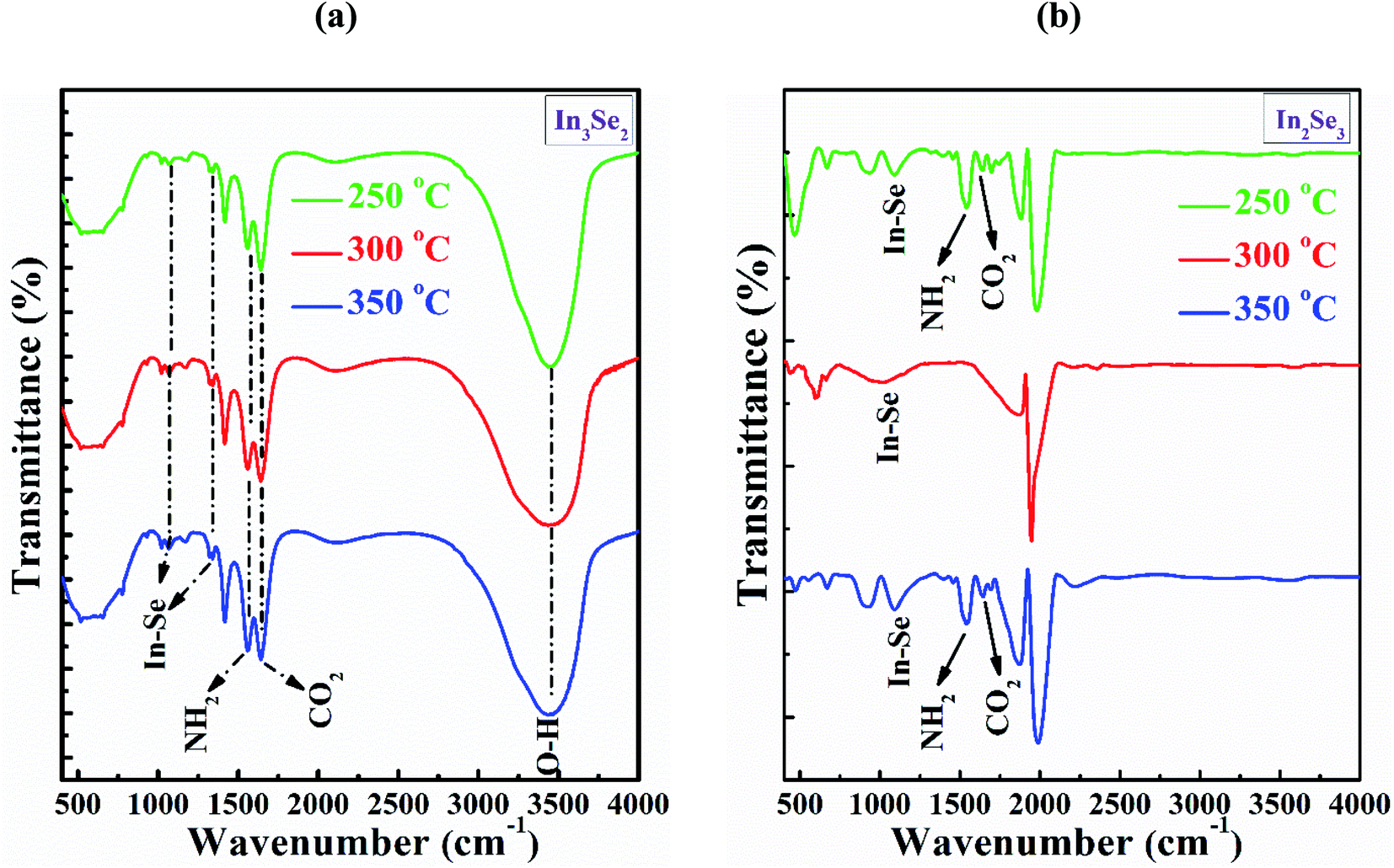 | ||
| Fig. 5 The FTIR spectra of InSe thin films for (a) In3Se2 and (b) In2Se3 phase, respectively deposited by spin coating method using thiol-amine cosolvents. | ||
Moreover, the peak intensity at the absorption band at 1090 cm−1 is found for the films annealed at 250 and 350 °C, respectively suggest the In–Se stretching vibration bonds of the of In2Se3 phase as shown in Fig. 5b. The small peaks at the absorption band at 1640 cm−1 are originated for CO2 molecule similar to In3Se2 phase.38,40 Another peak at the wavenumber 1022 cm−1 is also responsible for In–Se stretching vibration bond as appeared for the film annealed at 300 °C. The NH2 scissor vibrations bond is also identified at the absorption band at 1560 cm−1 for the annealing with stress which has come from cosolvents ethylene di-amine.39
3.3 The electrical properties of indium selenide thin films
Temperature dependent resistivity (ρ) of synthesized In3Se2 and In2Se3 thin films in the temperature range of 293–473 K are presented in Fig. 6a and b, respectively. Fig. S3 (a and b) in ESI† also presents temperature dependent conductivity (σ) in the range of 293–473 K of In3Se2 and In2Se3 thin films, respectively. It is noticed that for all samples the resistivity decreases with temperature which indicates the semiconducting nature of the films.4 It can also be seen that resistivity decreases significantly due to the application of stress in the samples during annealing. For the case of In3Se2 phase, the room temperature resistivity was in the magnitude of 104 (Ω cm) which decreased to 103 (Ω cm) at a temperature of 473 K for the films annealed at 250 and 300 °C, respectively as shown in Fig. 6a. However, the resistivity was in the order of 105 (Ω cm) for the films annealed at 350 °C and decreased to the order of 103 (Ω cm) at a temperature of 473 K. This difference in resistivity may be related to the surface morphology of the films as SEM images show that the In3Se2 films annealed at 350 °C is more discontinuous. On the other hand, the room temperature resistivity of In2Se3 phase was found in the order of 102 (Ω cm) for all annealing conditions and it decreased to the order of 101 (Ω cm) at a temperature of 473 K as shown in Fig. 6b. The In2Se3 thin films annealed at 300 °C exhibited less resistivity. This reduction of resistivity may also be associated with the surface morphology as SEM images show that the film annealed at 300 °C is relatively smooth and uniform compared to other samples leading to less carrier scattering effect.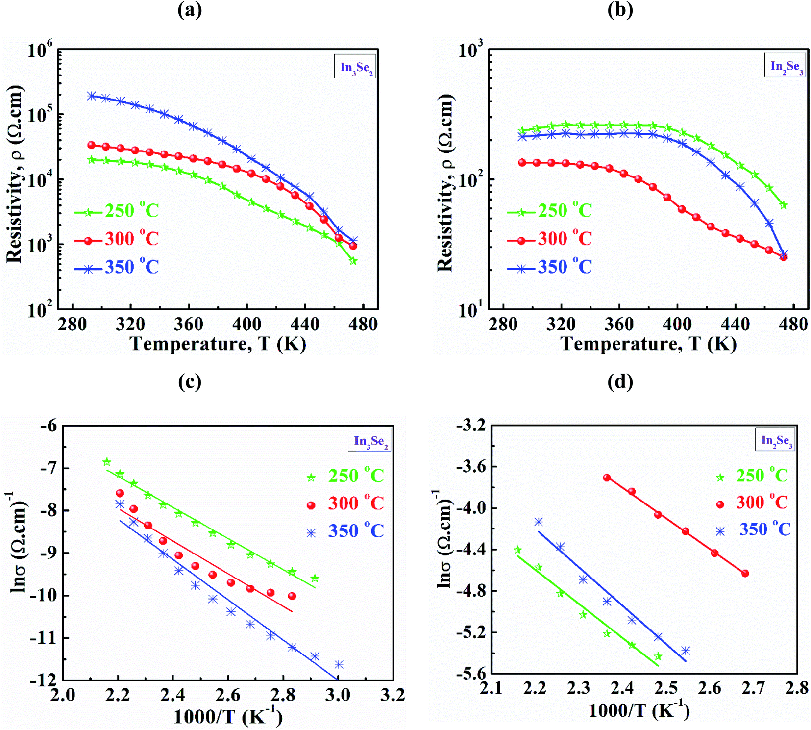 | ||
| Fig. 6 The temperature dependent electrical resistivity (a and b), variation of lnσ vs. T−1 of In3Se2 and In2Se3 thin films (c and d), respectively deposited by spin coating method using thiol-amine cosolvents. | ||
Fig. 6c and d depict the plots of lnσ vs. T−1 of In3Se2 and In2Se3 thin films, respectively for different annealed temperatures. The slopes of lnσ vs. T−1 plots are used to estimate the activation energies of In3Se2 and In2Se3 thin films using the following eqn (3)42
 | (3) |
| Annealing temperature (°C) | In3Se2 phase | In2Se3 phase | ||
|---|---|---|---|---|
| Activation energy, ΔEo (eV) | Pre-exponential factor, σo (Ω cm)−1 | Activation energy, ΔEo (eV) | Pre-exponential factor, σo (Ω cm)−1 | |
| 250 | 0.32 | 2.36 | 0.29 | 14.16 |
| 300 | 0.33 | 1.76 | 0.26 | 27.38 |
| 350 | 0.40 | 9.30 | 0.32 | 52.98 |
3.4 The optical properties of indium selenide thin films
The optical transmittance in the range of photon wavelength 360–1100 nm of spin coated In3Se2 and In2Se3 thin films for different annealing temperatures was measured as exhibited in Fig. 7a and b, respectively. It is observed from the figures that for both phases transmittance increases with increasing annealing temperature. When the samples are annealed at 350 °C, the β-In3Se2 phase of indium selenide thin films exhibit maximum transmittance which is significantly higher than the transmittance of the γ-In2Se3 samples. The transmittance of the β-In3Se2 samples with increasing annealing temperature can be correlated with the crystallinity and surface morphology of the films. As seen in XRD and SEM, better crystallinity and higher surface discontinuity was resulted for the sample annealed at 350 °C. Besides, the transmittance of the In2Se3 thin films also increases with annealing temperature which might be resulted due to the better crystallinity of the films with annealing temperature as shown in Fig. 7b. It can also be seen that for the both phases the transmittance decreases continuously with wavelength in the visible region from infrared region. This may happened due to the increasing of scattering loss in the visible region.34 It is also observed from the both figures that at wavelength around 676 nm there is a small unwanted bump which was generated due to instrumental error.46 The absorption spectra for both phases are shown in Fig. S4 in ESI.†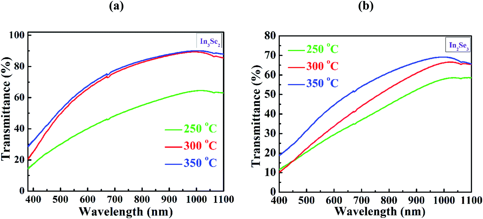 | ||
| Fig. 7 The optical transmittance spectra of spin coated (a) In3Se2 and (b) In2Se3 thin films, respectively prepared using thiol-amine co-solvents. | ||
The absorption coefficient, α was computed from the transmittance spectra using the following eqn (4).28
 | (4) |
The absorption coefficient was found in the order of 104 cm−1 for both phases which is also similar to earlier report.34
The absorption coefficient (α) and photon energy (hν) are related with the Tauc equation as47
| (αhν)2 = A(hν − Eg) | (5) |
Fig. 8a and b represent the Tauc plots of deposited In3Se2 and In2Se3 phases of indium selenide thin films, respectively for different annealing temperatures. In this work, the direct band gap of In3Se2 phases were found to be 2.60, 2.70 and 2.75 eV and that for In2Se3 phase were found to be 2.11 eV, 2.28 eV and 2.28 eV at annealing temperatures of 250, 300 and 350 °C, respectively. It is observed from the figures that band gap of both the phases increases with annealing temperatures. This increase in optical band gap with annealing temperature might occurred owing to the reduction of the disorder and defects in the structural bonding that were presented in the films. As the microstructural modifications in a thin film material rely on the growth kinetics and the substrate temperature, the uncompleted microstructures might be changed due to thermal energy of post-depositional annealing temperatures. The increase of optical band gap of indium selenide thin films due to annealing has already been reported.19,37,47 However, there are also few reports on nanostructured perovskite semiconductors indicating that band gap can be decreased through phase transformation and quantum confinement.48,49 The high band gap for In3Se2 phase at various annealing temperatures can be found in other reports.50,51 The band gap of In2Se3 phase is also agreed well with the reported values.52
 | ||
| Fig. 8 The Tauc plots of (a) In3Se2 and (b) In2Se3 phases of indium selenide thin films, respectively prepared using thiol-amine co-solvents showing the band gap of the films annealed at different temperatures. | ||
4. Conclusions
The indium selenide thin films have been synthesized by spin coating method using InSe solution in thiol-amine cosolvents. The films encounter phase transformation from β-In3Se2 to γ-In2Se3 phase due to a mechanical stress applied by 1–1.2 mm thick microscopic glass pressed with crocodile clips during annealing. The XRD study revealed the β-In3Se2 and γ-In2Se3 phases of synthesized indium selenide thin films without and with stress, respectively. The smooth and uniform surface were demonstrated by SEM micrographs for both phases. The EDS study showed the stoichiometric In3Se2 and In2Se3 phases. The In–Se stretching vibration bonds were noticed by FTIR study. Temperature dependent electrical study also revealed the non-degenerate indium selenide thin films for both phases. The transmittance spectra showed the maximum transmittance of approximately 77.5 and 54% at a wavelength of 700 nm for β-In3Se2 and γ-In2Se3 phases, respectively at an annealed temperature 350 °C. The absorption coefficient was found in the order of 104 cm1. The optical band gap was also calculated in the range of 2.60–2.75 and 2.12–2.28 eV for β-In3Se2 and γ-In2Se3 phases, respectively. These findings suggest that phase change in solution processed indium selenide might be applied in 2D optoelectronic devices in near future.Conflicts of interest
The authors declare no conflict of interests.Acknowledgements
The authors are indebted to Prof. Hajime Shirai and Mr Abdul Kuddus, Graduate School of Science and Engineering, Saitama University, Japan for providing facilities and help during thickness, XRD, FTIR and EDS measurements, respectively. The authors also highly appreciate Prof. Dr Md. Mahbubor Rahman, Dept of Chemistry, University of Rajshahi, Bangladesh for his help in FTIR result analysis in this work.References
- G. Gordillo and C. Calderon, CIS thin film solar cells with evaporated InSe buffer layers, Sol. Energy Mater. Sol. Cells, 2003, 77, 163–173 CrossRef CAS.
- G. M. Kumar, J. R. Kumar, P. Ilanchezhiyana, M. Paulraj, H. C. Jeona, D. Y. Kima and T. W. Kang, Photoelectrochemical analysis of shape modified γ-phase In2Se3 nanostructures photoelectrodes, J. Mater. Res. Technol., 2020, 9, 12318–12327 CrossRef.
- H. Lee, D.-H. Kang and L. Tran, Indium selenide (In2Se3) thin film for phase-change memory, Mater. Sci. Eng., B, 2005, 119, 196–201 CrossRef.
- J. Hossain, M. Julkarnain, B. K. Mondal, M. A. Newaz and K. A. Khan, Unveiling the electrical and thermoelectric properties of highly degenerate indium selenide thin films: indication of In3Se4 phase, Mater. Res. Express, 2019, 6, 126421 CrossRef CAS.
- A. F. El-Deeb, H. S. Metwally and H. A. Shehata, Structural and electrical properties of In6Se7 thin films, J. Phys. D: Appl. Phys., 2008, 41, 125305 CrossRef.
- M. Sznajder, K. Z. Rushchanskii, L. Yu. Kharkhalis and D. M. Bercha, Similarities of the band structure of In4Se3 and InSe under pressure and peculiarities of the creation of the band gap, Phys. Status Solidi B, 2006, 243, 592–609 CrossRef CAS.
- G. Han, Z.-G. Chen, C. Sun, L. Yang, L. Cheng, Z. Li, W. Lu, Z. M. Gibbs, G. J. Snyder, K. Jack, J. Drennan and J. Zou, A New Crystal: layer-structured rhombohedral In3Se4, CrystEngComm, 2014, 16, 393 RSC.
- G. Han, Q. Gu, L. Yang, Z.-G. Chen and J. Zou, A new indium selenide phase: controllable synthesis, phase transformation and photoluminescence properties, J. Mater. Chem. C, 2019, 7, 13573 RSC.
- F. I. Mustafa and M. Ali, InSe nano thin film with Ar–Gas at Low vacuum pressure, Appl. Mech. Mater., 2014, 606, 15–18 Search PubMed.
- X. F. Wei, L. W. Li, H. G. Feng, J. B. Gong, K. Jiang and S. L. Xue, Preparation and optical properties of In2Se3 nanospheres using CTAB as surface modifier, Ceram. Int., 2020, 46, 1026–1032 CrossRef CAS.
- X. Tao and Y. Gu, Crystalline-crystalline phase transformation in two-dimensionalIn2Se3 thin layers, Nano Lett., 2013, 13, 3501–3505 CrossRef CAS PubMed.
- M. Osman, Y. Huang, W. Feng, G. Liu, Y. Qiu and P. A. Hu, Modulation of opto-electronic properties of InSe thin layers via phase transformation, RSC Adv., 2016, 6, 70452–70459 RSC.
- B. K. Mondal, M. A. Newaz, M. A. Rashid, K. M. Hossain, S. K. Mostaque, M. F. Rahman, M. H. K. Rubel and J. Hossain, Electronic structure of In3−xSe4 electron transport layer for chalcogenide/p-Si heterojunction solar cells, ACS Omega, 2019, 4, 17762–17772 CrossRef CAS PubMed.
- J. Zhao and L. Yang, Structure evolutions and metallic transitions in In2Se3 under high pressure, J. Phys. Chem. C, 2014, 118, 5445–5452 CrossRef CAS.
- J. Hossain, M. Julkarnain, K. S. Sharif and K. A. Khan, Crystallization of e-beam evaporated amorphous InSe thin films after heat-treatment, Int. J. Renew. Energy Technol. Res., 2013, 2, 220–226 Search PubMed.
- I. H. Mutlu, M. Z. Zarbaliyev and F. Aslan, Indium selenide thin film preparation by sol–gel technique, J. Sol-Gel Sci. Technol., 2007, 43, 223–226 CrossRef CAS.
- H. Bouzouita, N. Bouguila, S. Duchemin, S. Fiechter and A. Dhouib, Preparation and characterization of In2Se3 thin films, Renewable Energy, 2002, 25, 131–138 CrossRef CAS.
- S. L. Stoll and A. R. Barron, Metal–organic chemical vapor deposition of indium selenide thin films, Chem. Mater., 1998, 10, 650–657 CrossRef CAS.
- C. Julien, N. Benramdane and J. P. Guesdon, Transformation steps of structure in flash-deposited films of a-InSe, Semicond. Sci. Technol., 1990, 5, 905–910 CrossRef CAS.
- J. Y. Emery, L. Brahim-Otsmane, M. Jouanne, C. Julien and M. Balkanski, Growth conditions of InxSey films by molecular beam deposition, Mater. Sci. Eng., B, 1989, 3, 13–17 CrossRef.
- O. Lang, A. Klein, C. Pettenkofer and W. Jaegermann, Band lineup of lattice mismatched InSe/GaSe quantum well structures prepared by van der waals epitaxy: absence of interfacial dipoles, J. Appl. Phys., 1996, 80, 3817–3821 CrossRef CAS.
- R. Panda, R. Naik and N. C. Mishra, Low-temperature growth of γ phase in thermally deposited In2Se3 thin films, Phase Transitions, 2018, 91, 862–871 CrossRef CAS.
- S. Gopal, C. Viswanathan, B. Karunagara, S. K. Narayandass, D. Mangalaraj and J. Yi, Preparation and characterization of electrodeposited indium selenide thin films, Cryst. Res. Technol., 2005, 40, 557–562 CrossRef CAS.
- R. E. Ornelas-Acosta, S. Shaji, D. Avellaneda, G. A. Castillo, T. K. Das Roy and B. Krishnan, Indium selenide thin films by laser irradiation of In/Se layered structure, Surf. Rev. Lett., 2013, 20, 1350058 CrossRef.
- C. L. Mccarthya and R. L. Brutchey, Solution processing of chalcogenide materials using thiol-amine alkahest solvent systems, Chem. Commun., 2017, 53, 4888–4902 RSC.
- D. H. Webber and R. L. Brutchey, Alkahest for V2VI3 chalcogenides:dissolution of nine bulk semiconductors in a diamine-dithiol solvent mixture, J. Am. Chem. Soc., 2013, 135, 15722–15725 CrossRef CAS PubMed.
- Z. Lin, Q. He, A. Yin, Y. Xu, C. Wang, M. Ding, H.-C. Cheng, B. Papandrea, Y. Huang and X. Duan, Cosolvent approach for solution processable electronic thin films, ACS Nano, 2015, 9, 4398–4405 CrossRef CAS PubMed.
- M. F. Rahman, J. Hossain, A. Kuddus, S. Tabassum, M. H. K. Rubel, H. Shirai and A. B. M. Ismail, A novel synthesis and characterization of transparent CdS thin films for CdTe/CdS solar cells, Appl. Phys. A, 2020, 126, 145 CrossRef CAS.
- F. I. Mustafa, S. Gupta, N. Goyal and S. K. Tripathi, Effect of indium concentration on the electrical properties of InSe alloy, Physica B, 2010, 405, 4087–4091 CrossRef CAS.
- P. B. Patel, H. N. Desai, J. M. Dhimmar and B. P. Modi, Micro-structural and thermoelectric characterization of zinc-doped In0.6Se0.4 crystal grown by direct vapour transport method, Semiconductors, 2020, 54, 923–928 CrossRef CAS.
- X. Tan, J. Zhou and Q. Yan, Ascorbic acid-assisted solvothermal growth of γ-In2Se3 hierarchical flowerlike architectures, CrystEngComm, 2011, 13, 2792 RSC.
- G. B. Williamson and R. C. Smallman, Dislocation densities in some annealed and cold-worked metals from measurements on the X-ray Debye–Scherrer spectrum, Philos. Mag., 1956, 1, 34 CrossRef CAS.
- X. Hong, T. S. Duffy, L. Ehm and D. J. Weidner, Pressure-induced stiffness of Au nanoparticles to 71 GPa under quasi-hydrostatic loading, J. Phys.: Condens. Matter, 2015, 27, 485303 CrossRef PubMed.
- P. Matheswaran, R. S. Kumar and R. Sathyamoorthy, Effect of annealing on the structural and optical properties of InSe bilayer thin films, Vacuum, 2011, 85, 820–826 CrossRef CAS.
- N. Balakrishnan, E. D. Steer, E. F. Smith, Z. R. Kudrynskyi, Z. D. Kovalyuk, L. Eaves, A. Patane and P. H. Beton, Epitaxial growth of γ-InSe and α,β, and γ-In2Se3 on ε-GaSe, 2D Mater., 2018, 5, 035026 CrossRef.
- J. Cui, H. Peng, Z. Song, Z. Du, Y. Chao and G. Chen, Significantly enhanced thermoelectric performance of γ-In2Se3 through lithiation via chemical diffusion, Chem. Mater., 2017, 29, 7467–7474 CrossRef CAS.
- M. Parlak and C. Erçelebi, The effect of substrate and post-annealing temperature on the structural and optical properties of polycrystalline InSe thin films, Thin Solid Films, 1998, 322, 334–339 CrossRef CAS.
- K. Ç. Demir, E. Demir, S. Yüksel and C. Coşkun, Influence of deposition conditions on nanostructured InSe thin films, Curr. Appl. Phys., 2019, 19, 1404–1413 CrossRef.
- P. Liu, S. Yu, W. Fan and W. Shi, A new inorganic–organic hybrid In2Se3(en) as hollow nanospheres: hydrothermal synthesis and near-infrared photoluminescence properties, Dalton Trans., 2013, 42, 2887 RSC.
- S. Yu, L. Shu, Y. Qian, Y. Xie, J. Yang and L. Yang, Hydrothermal preparation and characterization of nanocrystalline powder of beta-indium sulfide, Mater. Res. Bull., 1998, 33, 717–721 CrossRef CAS.
- J. O. Carneiro, F. Machado, L. Rebouta, M. I. Vasilevskiy, S. Lanceros-Méndez, V. Teixeira, M. F. Costa and A. P. Samantilleke, Compositional, optical and electrical characteristics of SiOx thin films deposited by reactive pulsed dc magnetron sputtering, Coatings, 2019, 9, 468 CrossRef CAS.
- M. Rahman, M. A. Newaz, B. K. Mondal, A. Kuddus, M. A. Karim, M. M. Rashid, M. H. K. Rubel and J. Hossain, Unraveling the electrical properties of solution-processed copper iodide thin films for CuI/n-Si solar cells, Mater. Res. Bull., 2019, 118, 110518 CrossRef CAS.
- R. W. Damgn and R. W. Redington, Electrical and optical properties of indium selenide, Phys. Rev., 1954, 96, 1498–1500 CrossRef.
- G. Micocci and A. Tepore, Electrical properties of vacuum-deposited polycrystalline InSe thin films, Sol. Energy Mater., 1991, 22, 215–222 CrossRef CAS.
- Q. Li and Y. S. Jun, The apparent activation energy and pre-exponential kinetic factor for heterogeneous calcium carbonate nucleation on quartz, Commun. Chem., 2018, 1, 56 CrossRef.
- M. A. Rashid, B. K. Mondal, M. H. K. Rubel, M. M. Rahman, O. T. Mefford and J. Hossain, Synthesis of self-assembled randomly oriented VO2 nanowires on a glass substrate by a spin coating method, Inorg. Chem., 2020, 59, 15707–15716 CrossRef CAS.
- J. Hossain, M. Julkarnain, K. S. Sharif and K. A. Khan, Optical properties of e-beam evaporated indium selenide (InSe) thin films, J. Sci. Res. Rep., 2014, 3, 1642–1655 Search PubMed.
- G. C. Adhikari, P. A. Vargas, H. Zhu and P. Zhu, Saponification precipitation method of CsPbBr3 nanocrystals with blue-green tunable emission, J. Phys. Chem. C, 2019, 123, 1406–1412 CrossRef CAS.
- G. C. Adhikari, P. A. Vargas, H. Zhu, A. Grigoriev and P. Zhu, Tetradic phosphor white light with variable CCT and superlative CRI through organolead halide perovskite nanocrystals, Nanoscale Adv., 2019, 1, 1791 RSC.
- A. Mohan and S. Rajesh, Impact of annealing on the investigation of In3Se2/Cu2Se/In3Se2 sandwich structure prepared by thermal evaporation technique for solar cell applications, Superlattices Microstruct., 2015, 85, 638–645 CrossRef CAS.
- A. Mohan, S. Rajesh and J. Suthagar, Temperature induced phase change in indium selenide thin films prepared by thermal evaporation technique, ATOM2014_28, UGC Sponsored National Conference on Advanced Technology Oriented Materials (ATOM-2014), 8–9th Dec- 2014, pp. 98-100 Search PubMed.
- K. Bindu, C. S. Kartha, K. P. Vijayakumar, T. Abe and Y. Kashiwaba, Structural, optical and electrical properties of In2Se3 thin films formed by annealing chemically deposited Se and vacuum evaporated In stack layers, Appl. Surf. Sci., 2002, 191, 138–147 CrossRef CAS.
Footnote |
| † Electronic supplementary information (ESI) available: Table for crystallite size and dislocation densities, EDS spectra, EDS mapping of γ-In2Se3, temperature dependent electrical conductivity and optical absorbance spectra of β-In3Se2 and γ-In2Se3 phases, respectively of indium selenide thin films. See DOI: 10.1039/d1ra01403j |
| This journal is © The Royal Society of Chemistry 2021 |