
 Open Access Article
 This Open Access Article is licensed under a Creative Commons Attribution-Non Commercial 3.0 Unported Licence
The use of sample positioning to control defect creation by oxygen plasma in isotopically labelled bilayer graphene membranes†
Valentino L. P. Guerra,
Václav Valeš,
Jiří Mikšátko,
Jan Plšek,
Karolina Anna Drogowska-Horná,
Oleksandr Volochanskyi and
Martin Kalbáč *
*
Department of Low-dimensional Systems, J. Heyrovský Institute of Physical Chemistry, Academy of Sciences of the Czech Republic, v.v.i., Dolejškova 3, 18223 Prague 8, Czech Republic. E-mail: martin.kalbac@jh-inst.cas.cz
First published on 10th March 2021
Abstract
Monolayer and isotopically labelled bilayer graphene membranes were prepared on grids for transmission electron microscopy (TEM). In order to create defects in the graphene layers in a controlled way, we studied the sensitivity of the individual graphene layers to the oxygen plasma treatment. We tested samples with different configurations by varying the order of the transfer of layers and changing the orientation of the samples with respect to the plasma chamber. Using Raman spectroscopy, HRTEM and X-ray photoelectron spectroscopy, we demonstrated defect formation and determined the quantity and chemical composition of the defects. By keeping the sample structure and the setup of the experiment unchanged, the significant role of the sample orientation with respect to the chamber was demonstrated. The effect was accounted for by the variation of the accessibility of the sample surface for the reactive species. Therefore, this effect can be used to control the degree of damage in each layer, resulting in differing numbers of defects present on each side of the sample.
1 Introduction
The defects in graphene influence many important properties, including reactivity, transport and strength.1 They can be used to induce new functionality to graphene; for example, if they are formed within the graphene membrane. Controlling the defects in graphene layers is thus an important but still challenging task.Raman spectroscopy plays a key role in characterising defects because it enables their fast and easy quantification. The most prominent Raman modes in graphene are the D, G, D′ and 2D bands. The D and D′ modes are associated with the presence of sp3 carbon atoms.2 The G mode originates from the doubly degenerate phonon mode in the centre of the Brillouin zone, and the symmetry-allowed 2D mode originates from a second-order process involving two transverse optical phonons.3 From the beginning of the study of graphene, the so-called D mode in the Raman spectra has been used to evaluate the number of defects. The D mode originates from a second-order process which involves an intervalley phonon with a large momentum and its interaction with the defect. The intensity of the D mode corresponds to the number of defects,2 but provides only a little information about the defect quality. The D′ mode involves the interaction of an intravalley phonon and the defect, and it has been suggested that its intensity correlates with specific types of defects.4,5 Other spectroscopic and microscopic approaches have been employed to complement the Raman spectroscopy data; including X-ray photoelectron spectroscopy (XPS) and high-resolution transmission electron microscopy (HRTEM). However, it is very difficult to extract the information about defect content for the individual layers of graphene from these latter methods, for samples conatining more than one graphene layer. In contrast, Raman spectroscopy combined with isotope labelling of graphene layers can be used to evaluate the number of defects in graphene bilayers or potentially even trilayers,6 because the Raman shift is dependent on the mass of the vibrating atom. Consequently, the frequencies of the Raman modes of 13C graphene are significantly downshifted from the frequencies of the 12C modes. This is also true for the D mode, and thus the D modes of different isotopically labelled layers can be distinguished.6 In the case of AB stacked bilayers7 the evaluation of the number of defects can be significantly affected by scattering of the phonons from one layer by defects in the second layer. Nevertheless, in non-interacting layers, the evaluation of the number of defects is affected only a little.8
In the literature, defects in graphene induced by Ar ions have been quantified by Raman spectroscopy, namely using the D/G ratio.2,9 With increasing defect density (nD), the D/G ratio increases; however, at a certain defect density, the D/G ratio reaches a maximum value and decreases with further increase in nD. Such a regime of high defect density is accompanied by an increasing D band width and disappearance of the 2D band. The dependence of the D/G radio on nD depends also on the phenomenological parameters of the defects and the energy of the excitation laser.
The defects in graphene can be created in different ways, for example, above mentioned ion bombardment.10 Furthermore, we recently demonstrated how the pulsed laser deposition of ceria nanoparticles on graphene could induce the formation of defects.11 Another method that leads to local defects is the application of the electron beam in the HRTEM. These approaches require relatively demanding instrumentation or are not efficient for creating defects on a larger scale. Other approaches involve UV–ozone or oxygen plasma treatment.8 The latter approach is very simple, fast, and efficient; it can be easily applied on a large scale. The drawback of this approach is the limited control of the process, which leads to variable results in the literature.12–14 Successfully addressing this issue can thus enable or promote several applications of porous graphene membranes.
The defect creation is closely connected with functionalization of graphene by different functional groups because the defects produced by plasma exposure can be not only structural (i.e. missing carbon atom) but also functional (sp3-like defects interacting with an external atom/molecule). Experimental and theoretical studies showed that C–O–C epoxy groups are dominant species formed on the graphene surfaces.15,16 On more defective surfaces the interaction with oxygen atoms leads to the formation of other functional groups such as carbonyl or carboxyl groups.17 When functional groups are present, the carbon atoms which are in their close proximity may show increased reactivity (like in the case of the oxygen).18
In this study, we explored the effect of the positioning of the graphene bilayers in the reaction chamber with respect to the oxygen plasma on the number of created defects. In agreement with previous studies, our results indicated that the creation of defects in suspended graphene is more difficult than in graphene on the substrate. In addition, the orientation of the TEM grid with the graphene bilayer with respect to the plasma chamber significantly affected the number of defects created in the top and bottom layers of the graphene bilayer. The number of defects was estimated by Raman spectroscopy, and the samples were further characterised by XPS and HRTEM.
2 Experimental
2.1 Graphene synthesis and transfer
Graphene was grown by the chemical vapour deposition method (CVD) as described in earlier work.19 In brief, polycrystalline copper foil was annealed under 50 sccm flow of H2 for 20 minutes, then 1 sccm flow of 12CH4 (99.9995%, natural isotopic composition, Air Liquide) or 13CH4 (min 99 atom% 13C, Isotec) was introduced. The graphene growth was maintained for 35 minutes and finally annealed again in a pure H2 atmosphere for five minutes. The pressure during the whole process was 350 mTorr.After cooling to room temperature, graphene was transferred onto gold TEM grids (SPI Supplies, 2000 mesh) by the nitrocellulose assisted method.20 In brief, the graphene remaining on the copper was covered by spin coating nitrocellulose (Collodion solution, Sigma-Aldrich), followed by O2 plasma etching of the graphene exposed from the other side of the copper foil. The sample was then cut into several pieces of a suitable size for the transfer. All these pieces were allowed to float on the surface of a copper etchant bath (FeCl3 with HCl, Transene) until no residual copper was visible under the floating polymeric film. Using a piece of Si/SiO2 wafer as a support, the samples were recovered from the copper etchant and moved into a 0.1 M solution of HCl in H2O as an initial cleaning step, followed by multiple transfers in demineralised water (MilliQ) to complete the cleaning. After the final water bath, a gold grid for TEM (2000 mesh) was used to collect the graphene from the water. Samples were then dried at a 45° angle on a hotplate set at 60 °C for ten minutes21 and subsequently washed by multiple rinses with hot methanol. For a few samples, we used a silicon wafer as the substrate; in that case, the Si/SiO2 wafer was used to collect the graphene from the water. The samples were then dried by blowing Ar perpendicularly to the surface and washed by rinsing the sample multiple times in hot methanol.
In order to produce isotopically labelled graphene bilayers, the transfer of graphene was performed twice for each grid. The samples were prepared by transfer of the 12C graphene and then 13C graphene or vice versa (see sample designations in Fig. 2).
The freshly obtained free-standing bilayer graphene was subsequently investigated by Raman spectroscopy, HRTEM and XPS.
2.2 Oxygen plasma treatment
For the oxygen plasma treatment, we used an oxygen plasma etcher (PICO, Diener Plasma-Surface Technology). First, the chamber was pumped to low pressure (0.3 mbar), then a controlled flow of oxygen (20 sccm) was used to fill the chamber with O2 and to stabilise the pressure (0.77 mbar). At this point, the plasma was turned on (350 W) for the duration of the plasma treatment. Afterwards, the plasma chamber was purged with nitrogen and finally opened to atmosphere. The samples treated by O2 plasma were then investigated by Raman spectroscopy, HRTEM and XPS.2.3 Raman spectroscopy
Raman spectroscopy measurements were performed with a Witec Alpha300 R spectrometer equipped with a piezo stage using a 532 nm excitation wavelength. The laser power was kept below 1 mW in order to avoid any heating effects. The laser spot was focused on the sample with a 100× objective and had a diameter of approximately 500–1000 nm.2.4 High resolution transmission electron microscopy (HRTEM)
The HRTEM images were acquired on a JEOL JEM-2100Plus microscope with an acceleration voltage of 100 kV.2.5 X-ray photoelectron spectroscopy (XPS)
The XPS measurements were performed in a Phoibos 150 Specs spectrometer with a base pressure lower than 10−9 mbar. A monochromatic Al Kα radiation source with a spot size of 1 mm2 was used to excite the electrons. The pass energy of the electron energy analyser was set at 20 eV. The take-off angle between the analysed photoelectrons and the substrate surface was 90°.3 Result and discussion
To find suitable conditions for the plasma treatment, several single-layer graphene samples were tested before moving to the bilayer graphene membranes (Fig. 1). As a starting point, we used the same conditions as in ref. 1, but we observed that the graphene supported by the TEM grid was less damaged by the plasma than the graphene on the Si/SiO2 substrate. The difference can be clearly seen in Fig. S1 (ESI†). Treatments with a duration of ten seconds or less did not show sufficient increases in the graphene D band, which we used to track the number of defects induced to the graphene layer. As shown in Fig. 1, a substantial increase in the D band of graphene was obtained after 50 seconds of treatment, together with the appearance of the D′ band.4,5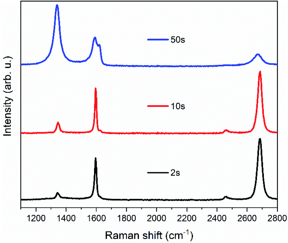 | ||
| Fig. 1 Raman spectra of plasma-treated single-layer graphene (12C). The samples were transferred onto a gold TEM grid and then treated for 2, 10, 50 seconds (from bottom to top) in the plasma chamber at 0.77 mbar and 35% power (350 W). | ||
For the analysis of bilayer graphene samples, we labelled the individual layers using two different kinds of graphene: one grown from natural 12C and one from carbon isotopically enriched in 13C (99%).6 In this way, we were able to follow the Raman bands of each layer independently because the Raman peaks of the 13C graphene layer are shifted with respect to the 12C positions. The G and 2D modes are found at around 1595 cm−1 and 2670 cm−1 for 12C and around 1535 cm−1 and 2580 cm−1 for 13C. Similarly for the D and D′ band, which are located around 1350 cm−1 and 1625 cm−1 for 12C and around 1300 cm−1 and 1565 cm−1 for 13C.
The Raman spectroscopy of the samples before plasma treatment confirmed the presence of graphene bilayers (Fig. S2 in ESI†) without any significant D bands. The samples were then exposed to the oxygen plasma (i) horizontally while laying on a Si/SiO2 substrate or (ii) vertically while held in a pair of tweezers (designated as Au-12-13-V-50s). We prepared four horizontal samples (designated as Au-12-13-H-50s, 13-12-Au-H-50s, 12-13-Au-H-50s, and Au-13-12-H-50s), varying both the order of the individual graphene layers on the TEM grid and the orientation of the whole grid in the plasma chamber (Fig. 2).
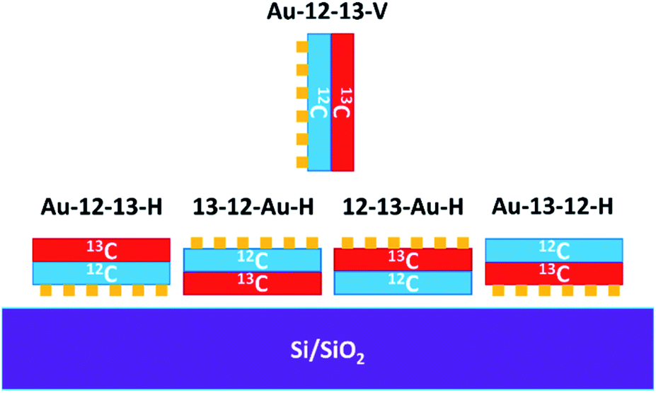 | ||
| Fig. 2 Schematic representation of the orientation of the samples as loaded in the plasma chamber. | ||
Typical Raman spectra of the graphene bilayer membranes after oxygen plasma treatment are shown with fits in Fig. 3. It can be seen that the spectra of 13-12-Au-H and 12-13-Au-H show significant differences. For further analysis, median values with dispersion described by the first and third quartile obtained from Raman spatial maps were considered. Fig. S3 (in ESI†) displays the spatial distribution of the D/G ratios in the Raman maps, confirming a uniform distribution of defects within the same graphene layer.
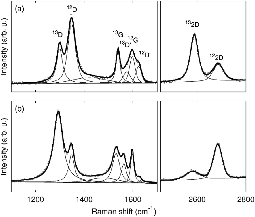 | ||
| Fig. 3 Typical spectra and fits of the samples (a) 13-12-Au-H and (b) 12-13-Au-H. | ||
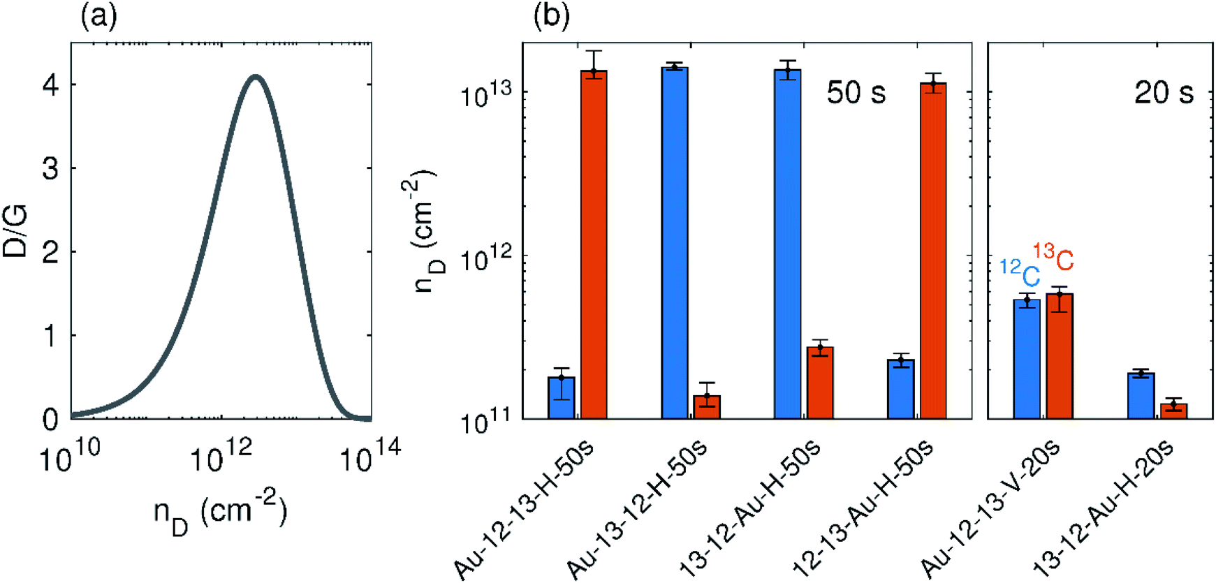
The positioning of the graphene bilayer in plasma chamber plays a crucial role in the degree of sample damage. The damage to the vertically aligned sample Au-12-13-V-50s was so substantial that no graphene was left on the grid after the treatment. In order to better evaluate the influence of the orientation in the plasma chamber, another set of two samples that were plasma treated for only 20 seconds were prepared and analysed (designated as Au-12-13-V-20s and 13-12-Au-H-20s). The statistically relevant parameters for all the samples obtained from Raman maps are summarised in Fig. 4.
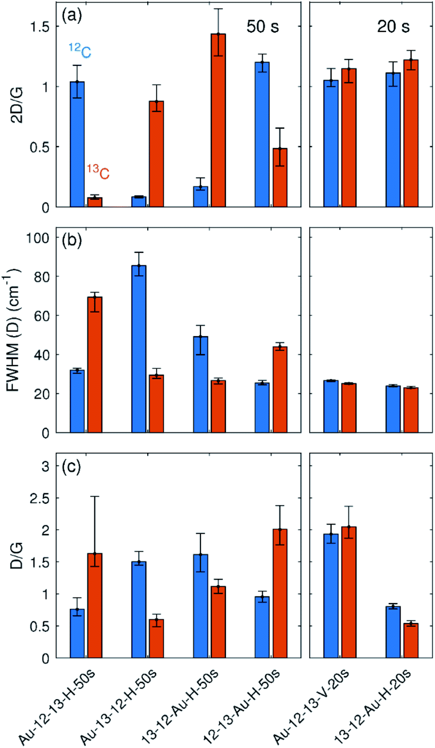 | ||
| Fig. 4 Parameters extracted from the fitted Raman maps. (a) The intensity ratio between 2D and G bands. (b) The full width at half maximum of the D band. (c) The intensity ratio between D and G bands. Data from 12C and 13C are labelled with blue and orange colours respectively. | ||
In the samples with a treatment time of 50 s, all of the horizontally placed samples show the similar results regardless of their position relative to the gold grid. The top layers of all samples show a higher density of defects than the bottom layers, which is also evident because of a dramatic decrease of the 2D band intensity. Because these top layers also exhibit wider D bands, the defect density is not directly proportional to the D/G intensity ratio.2 With increasing defect density, the D/G ratio starts to decrease at a certain point (Fig. 5(a)). According to this dependence, two regimes can be distinguished: a low defect density regime for defect density up to ∼2.5 × 1012 cm−2 and a high defect density regime for defect density above 2.5 × 1012 cm−2. For samples treated by 50 seconds of plasma, the D/G ratio for the top layer falls into the high defect density regime; however, the D/G ratio for the second layer falls in the low defect density regime. Direct comparison of the D/G ratio of both layers can thus be confusing. Therefore, it is necessary to perform defect evaluation after converting the D/G ratio to the defect density. Following the phenomenological dependence of the D/G ratio on the defect density and taking into account the width of the D band and the intensity of the 2D band, the defect density can finally be estimated (Fig. 5(b)).
 | ||
| Fig. 5 (a) Phenomenological dependence of ID/IG on the defect density, nD, adapted from ref. 2. (b) The defect densities in individually labelled layers of studied samples. Data from 12C and 13C are labelled with blue and orange colours respectively. | ||
In the samples treated for 20 s, the horizontal sample 13-12-Au-H-20s shows much less oxygen plasma-induced damage than the horizontal samples treated for 50 s (Fig. 4 and 5(b)). Vertical sample Au-12-13-V-20s contains almost the same number of defects for both layers and for each of them the defect density is much higher than the horizontal sample (note that the samples were treated together). This increase can be understood by considering that in the vertically placed sample both graphene layers are accessible directly by the plasma and defects are created in addition by the penetration of oxygen reactive species through the first layer, and so are added to both layers equally. For horizontally placed samples, only the top layer is exposed directly, while the defects in bottom layer are assumed to appear mainly from areas where large defects in the top layer have already formed.
The horizontal and vertical samples exposed to oxygen plasma for 20 s (Fig. 6) exhibit overall lower numbers of defects and fall in the low defect density region (Fig. 5(a)). Therefore the nature of the defects can be suggested from the D/D′ ratio according to the existing literature.4,5 The D/D′ ratio of Au-12-13-V-20s sample is between 7–8 for both graphene layers. In the horizontal sample 13-12-Au-H-20s, the top layer shows a slightly higher D/D′ ratio, around 9, while the bottom layer shows the ratio is around 7 (Fig. 6(b)). This value of the D/D′ ratio suggests the presence of sp3 carbon induced by vacancies in the graphene structure. A higher ratio (∼13) indicates the presence of sp3 carbon atoms induced by bonded species.4,5 Our results, therefore, indicate the presence of pores in both layers of the graphene membrane.
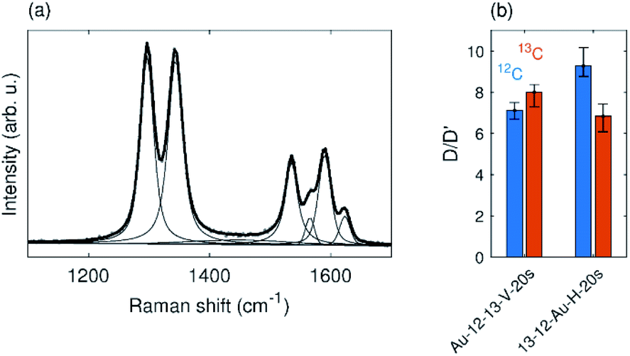 | ||
| Fig. 6 (a) Typical spectrum of Au-12-13-V-20s sample. (b) D/D′ ratio of samples that were plasma treated for 20 s. | ||
HRTEM analysis of the as prepared bilayer graphene membranes does not show any significant variation in contrast, which suggests that the membrane is generally intact on the larger scale. Furthermore, the difference in contrast along the boundaries of mesoscopic defects in one of the graphene layers is visible (Fig. S4†). This means that possible pores in even one layer of the bilayer graphene membrane would be observable. In contrast to the as-transferred bilayer graphene (Fig. 7(a)), HRTEM analysis of the plasma-treated membrane reveals a series of randomly distributed small bright dots a few nanometres in diameter (Fig. 7(d), red lines). Such structures can be attributed to holes, which represent the vacancy defects caused by the oxygen plasma. It is not possible to determine from the TEM analysis which layer is more affected by the oxygen plasma; however, the presence of vacancy defects in the structure of the plasma-treated membrane is apparent from the images obtained. Fig. 7 shows the development of holes under irradiation by focusing the electron beam on the same point for several minutes. Since this exposure results in beam induced damage to the membrane, this condition was used only for few dedicated samples to actually prove the possibility to visually distinguish the holes by their contrast and their evolution in time. For the as-transferred sample (Fig. 7(a–c)) it takes more than three minutes of exposure for evidence of the beam-induced formation of defects to become visible. In the sample treated with oxygen plasma instead (Fig. 7(d–f)), the holes that were already present at the beginning grow due to the effect of the electron beam, it is in fact possible to track some of them and follow their enlargement, confirming that they were actually holes and not artefacts.
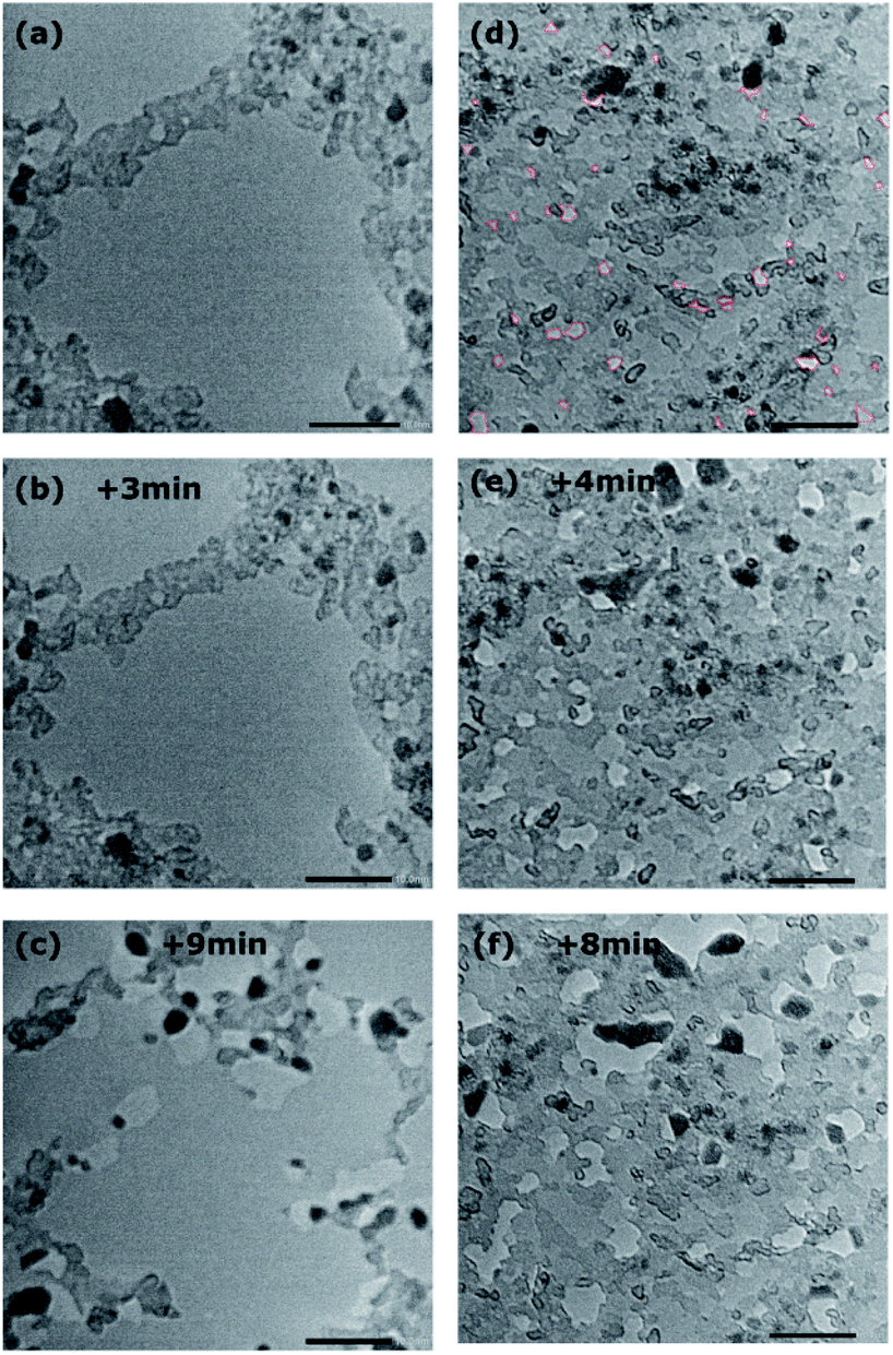 | ||
| Fig. 7 Comparison of HRTEM images of as-transferred and plasma-treated bilayer graphene. In (a) the as-transferred sample, with time evolution of the same area after (b) 3 minutes and (c) 9 minutes exposure. In (d) the plasma-treated sample, with time evolution of the same area after (e) 4 minutes and (f) 8 minutes exposure. All scale bars are 10 nm. In (d) holes are marked with a red dashed line along the edges. | ||
The effects of the plasma treatment on the graphene membranes were also investigated by XPS. The C 1s spectra of the pristine and plasma-treated samples (Fig. 8) were fitted by seven components: C1–C7. The component labelled C1 at ∼284.38 eV was modelled using a simplified asymmetric peak shape,22 and it is assigned to the sp2 hybridised carbon states. The weak shake-up satellite peak (labelled as C7), which corresponds to the C1 peak, was fitted at a fixed separation of 6.2 eV from the C1 component. Parameters used for the C1 asymmetric peak shape and the separation of the C7 peak were determined by fitting data collected from an as-grown CVD graphene on Cu foil. The component C2 at ∼284.9 eV can be attributed to sp3 defects in graphene, non-aromatic C atoms or CH bonding. The component C3 at ∼286.5 eV is assigned to the C–O functional group. The component C4 at ∼287.2 eV is attributed to the C–ONO2 nitrate ester groups23,24 The latter two components belong mainly to carbon atoms in the residues of nitrocellulose from the graphene transfer procedure (for confirmation of the presence of nitrocellulose, see the N 1s spectra in Fig. S5†). The other smaller components, C5 and C6 at ∼288.3 and ∼289.45 eV, are related to the carbonyl (C![[double bond, length as m-dash]](https://www.rsc.org/images/entities/char_e001.gif) O) and carboxyl groups (OC–O). The assignments of oxygen functional groups are in qualitative agreement with the literature25–28 even though there is some uncertainty in the exact binding energy value for individual components. It should be noted that the presence of impurities did not allowed reasonable evaluation of O 1s spectra.
O) and carboxyl groups (OC–O). The assignments of oxygen functional groups are in qualitative agreement with the literature25–28 even though there is some uncertainty in the exact binding energy value for individual components. It should be noted that the presence of impurities did not allowed reasonable evaluation of O 1s spectra.
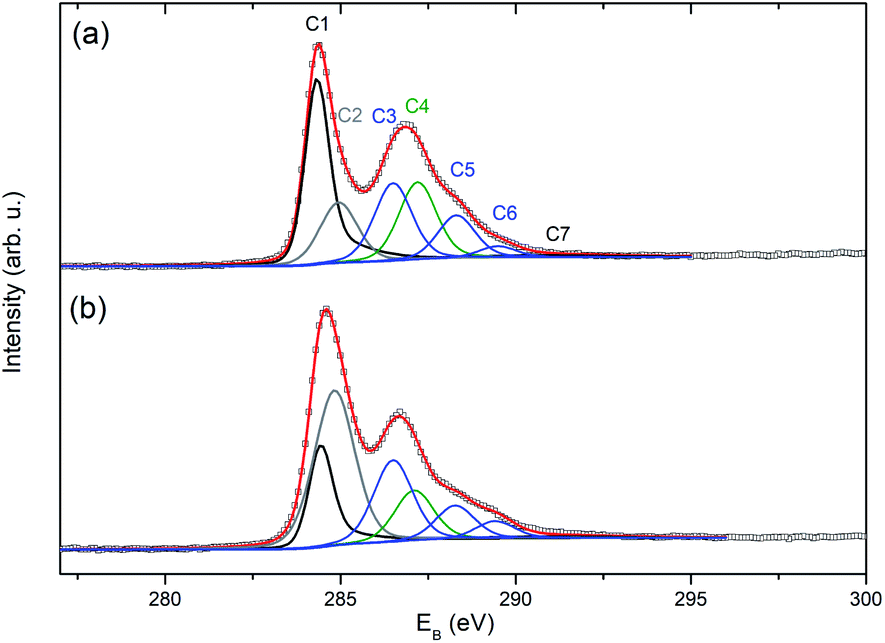 | ||
| Fig. 8 Fitted spectra of C 1s photoelectrons obtained for the sample 13-12-Au-H (a) before and (b) after plasma treatment. | ||
The plasma treatment resulted in partial nitrocellulose decomposition indicated by a substantial decrease in the intensity of the N 1s photoelectrons (see Fig. S5†) and the C4 component in the C 1s spectrum (Fig. 8(b)). The main impact of the plasma treatment on graphene is the decrease of the C1 component (sp2) by about 50% together with a more than double increase of the C2 component. This change can be explained by an increase in the population of sp3 carbon atoms, non-aromatic carbon atoms and/or hydrogenated carbon atoms to the detriment of the sp2 carbon atoms. Despite the continued presence of nitrocellulose residues (see Fig. S5†) and consequently the occurrence of their components in the C 1s spectrum, the presence of oxygen-containing C–O and OC–O functional groups on the graphene can be judged by the relative increase of C3 and C6 components (Fig. 8).
4 Conclusions
We prepared monolayer and isotopically labelled bilayer graphene membranes on TEM grids, studied the sensitivity of the individual graphene layers to oxygen plasma treatment and proposed a more controlled method to create defects in the graphene layers. For samples held parallel to the plasma base, the bottom graphene layers have fewer defects than the top layers. If the sample is oriented perpendicular to the plasma chamber base (so both sites are accessible) the number of defects is similar for both the top and bottom graphene layers. Simultaneously, the defects are created more efficiently for the latter samples than in the former ones. The defects created in the graphene bilayers were imaged using HRTEM, and it was demonstrated that the defects increase in size with increasing duration of the imaging in the HRTEM. X-ray photoelectron spectroscopy showed that the oxygen plasma treatment contributes to cleaning residues from the transfer of the sample (nitrocellulose) and at the same time, confirmed the presence of oxygen-containing C–O and OC–O functional groups on the graphene. We demonstrated the importance of the control of the sample positioning during the oxygen plasma treatment, which can be used as a simple yet very effective tool for creating defects in graphene multilayers. Also, the defect creation was reproducible and thus the method was reliable. Due to this approach, it is possible to control the relative number of defects generated in each layer of a bilayer graphene membrane, resulting in a controlled method for tuning the density of defects present on the chosen side of the sample.
Author contributions
VLPG and MK proposed and supervised the project; VLPG, VV and JP designed the experiments; VLPG prepared the membranes and performed oxygen plasma; VLPG performed Raman spectroscopy and VV analysed the data; JP performed XPS and analysed the data; JM performed HRTEM and analysed the data; OV and KAD-H prepared the graphene and provided the materials. VLPG, VV, JP and MK wrote the manuscript; all the authors contributed to the discussion of the results and commented the manuscript. All authors have given approval to the final version of the manuscript.Conflicts of interest
There are no conflicts to declare.Acknowledgements
The project was funded by Czech Science foundation (20-08633X). The authors thank Mrs Ilona Spirovová for the technical help and fitting of the Raman spectra and Mr Vaclav Protiva for the technical help and acquisition of TEM pictures. The work was further supported by European Regional Development Fund; OP RDE; project: “Carbon allotropes with rationalized nanointerfaces and nanolinks for environmental and biomedical applications” (No. CZ.02.1.01/0.0/0.0/16_026/0008382).References
- S. D. Costa, J. E. Weis, O. Frank, M. Fridrichová, Z. Bastl and M. Kalbac, RSC Adv., 2016, 6, 81471–81476 RSC.
- L. G. Cançado, A. Jorio, E. H. M. Ferreira, F. Stavale, C. A. Achete, R. B. Capaz, M. V. O. Moutinho, A. Lombardo, T. S. Kulmala and A. C. Ferrari, Nano Lett., 2011, 11, 3190–3196 CrossRef PubMed.
- L. M. Malard, M. A. Pimenta, G. Dresselhaus and M. S. Dresselhaus, Phys. Rep., 2009, 473, 51–87 CrossRef CAS.
- A. Eckmann, A. Felten, A. Mishchenko, L. Britnell, R. Krupke, K. S. Novoselov and C. Casiraghi, Nano Lett., 2012, 12, 3925–3930 CrossRef CAS PubMed.
- J. Jiang, R. Pachter, T. Demeritte, P. C. Ray, A. E. Islam, B. Maruyama and J. J. Boeckl, J. Phys. Chem. C, 2016, 120, 5371–5383 CrossRef CAS.
- O. Frank, L. Kavan and M. Kalbac, Nanoscale, 2014, 6, 6363–6370 RSC.
- W. Fang, A. L. Hsu, R. Caudillo, Y. Song, A. G. Birdwell, E. Zakar, M. Kalbac, M. Dubey, T. Palacios, M. S. Dresselhaus, P. T. Araujo and J. Kong, Nano Lett., 2013, 13, 1541–1548 CrossRef CAS.
- S. D. Costa, J. Ek Weis, O. Frank and M. Kalbac, Carbon, 2016, 98, 592–598 CrossRef CAS.
- M. M. Lucchese, F. Stavale, E. H. M. Ferreira, C. Vilani, M. V. O. Moutinho, R. B. Capaz, C. A. Achete and A. Jorio, Carbon, 2010, 48, 1592–1597 CrossRef CAS.
- M. Kalbac, O. Lehtinen, A. V. Krasheninnikov and J. Keinonen, Adv. Mater., 2013, 25, 1004–1009 CrossRef CAS PubMed.
- J. Plšek, K. A. Drogowska-Horná, V. L. P. Guerra, J. Mikšátko, K. A. Drogowská-Horná, V. Valeš and M. Kalbac, Chem.–Eur. J., 2021, 27, 4150–4158 CrossRef PubMed.
- T. Gokus, R. R. Nair, A. Bonetti, M. Böhmler, A. Lombardo, K. S. Novoselov, A. K. Geim, A. C. Ferrari and A. Hartschuh, ACS Nano, 2009, 3, 3963–3968 CrossRef CAS PubMed.
- I. Childres, L. A. Jauregui, J. Tian and Y. P. Chen, New J. Phys., 2011, 13, 025008 CrossRef.
- Z. Li, Y. Xu, B. Cao, L. Qi, S. He, C. Wang, J. Zhang, J. Wang and K. Xu, Superlattices Microstruct., 2016, 99, 125–130 CrossRef CAS.
- A. Barinov, O. B. Malcioǧlu, S. Fabris, T. Sun, L. Gregoratti, M. Dalmiglio and M. Kiskinova, J. Phys. Chem. C, 2009, 113, 9009–9013 CrossRef CAS.
- J. E. Johns and M. C. Hersam, Acc. Chem. Res., 2013, 46, 77–86 CrossRef CAS PubMed.
- D. Chen, H. Feng and J. Li, Chem. Rev., 2012, 112, 6027–6053 CrossRef CAS.
- P. A. Denis and C. Pereyra Huelmo, Carbon, 2015, 87, 106–115 CrossRef CAS.
- M. Kalbac, O. Frank and L. Kavan, Carbon, 2012, 50, 3682–3687 CrossRef CAS.
- T. Hallam, N. C. Berner, C. Yim and G. S. Duesberg, Adv. Mater. Interfaces, 2014, 1, 1400115 CrossRef.
- G. Goyal, Y. B. Lee, A. Darvish, C. W. Ahn and M. J. Kim, Nanotechnology, 2016, 27, 495301 CrossRef PubMed.
- R. W. M. Kwok, XPS Peak Fitting Program for WIN95/98 XPSPEAK, Version 4.1, Department of Chemistry, The Chinese University of Hong Kong, rmkwok@cuhk.edu.hk Search PubMed.
- A. H. K. Fowler, H. S. Munro and D. T. Clark, Polym. Degrad. Stab., 1985, 11, 287–296 CrossRef CAS.
- D. T. Clark and P. J. Stephenson, Polymer, 1982, 23, 1034–1038 CrossRef CAS.
- Y. Wei, Z. Pastuovic, T. Murphy and D. B. Gore, Appl. Surf. Sci., 2020, 505, 144651 CrossRef CAS.
- L. G. Vanquickenborne, J. Vranckx and C. Goeller-Walrand, J. Am. Chem. Soc., 1974, 96, 4121–4125 CrossRef CAS.
- A. Ganguly, S. Sharma, P. Papakonstantinou and J. Hamilton, J. Phys. Chem. C, 2011, 115, 17009–17019 CrossRef CAS.
- S. Stankovich, R. D. Piner, X. Chen, N. Wu, S. T. Nguyen and R. S. Ruoff, J. Mater. Chem., 2006, 16, 155–158 RSC.
Footnote |
| † Electronic supplementary information (ESI) available. See DOI: 10.1039/d1ra01249e |
| This journal is © The Royal Society of Chemistry 2021 |