
 Open Access Article
 This Open Access Article is licensed under a Creative Commons Attribution-Non Commercial 3.0 Unported Licence
Fabrication of ring oscillators using organic molecules of phenacene and perylenedicarboximide
Niko Fioravantia,
Luca Pierantonia,
Davide Mencarellia,
Claudio Turchetti*a,
Shino Hamaob,
Hideki Okamoto c,
Hidenori Gotob,
Ritsuko Eguchib,
Akihiko Fujiwarad and
Yoshihiro Kubozono*b
c,
Hidenori Gotob,
Ritsuko Eguchib,
Akihiko Fujiwarad and
Yoshihiro Kubozono*b
aDepartment of Information Engineering, Università Politecnica della Marche, Ancona I-60131, Italy
bResearch Institute for Interdisciplinary Science, Okayama University, Okayama 700-8530, Japan. E-mail: kubozono@cc.okayama-u.ac.jp
cDivision of Earth, Life and Molecular Sciences, Okayama University, Okayama 700-8530, Japan
dDepartment of Nanotechnology for Sustainable Energy, Kwansei Gakuin University, Sanda 669-1337, Japan
First published on 16th February 2021
Abstract
Organic field-effect transistors (FETs) can be applied to radio-frequency identification tags (RFIDs) and active-matrix flat-panel displays. For RFID application, a cardinal functional block is a ring oscillator using an odd number of inverters to convert DC voltage to AC. Herein, we report the properties of two ring oscillators, one formed with [6]phenacene for a p-channel FET and N,N′-dioctyl-3,4,9,10-perylenedicarboximide (PTCDI-C8) for an n-channel FET, and one formed with 3,10-ditetradecylpicene ((C14H29)2-picene) for a p-channel FET and PTCDI-C8 for an n-channel FET. The former ring oscillator provided a maximum oscillation frequency, fosc of 26 Hz, and the latter a maximum fosc of 21 Hz. The drain–drain voltage, VDD, applied to these ring oscillators was 100 V. This may be the first step towards a future practical ring oscillator using phenacene molecules. The values of field-effect mobility, μ in the p-channel [6]phenacene FET and n-channel PTCDI-C8 FET, which form the building blocks in the ring oscillator with an fosc value of 26 Hz, are 1.19 and 1.50 × 10⁻¹ cm2 V−1 s−1, respectively, while the values in the p-channel (C14H29)2-picene FET and n-channel PTCDI-C8 FET, which form the ring oscillator with an fosc of 21 Hz, are 1.85 and 1.54 × 10⁻¹ cm2 V−1 s−1, respectively. The μ values in the p-channel FETs are higher by one order of magnitude than those of the n-channel FET, which must be addressed to increase the value of fosc. Finally, we fabricated a ring oscillator with ZrO2 instead of parylene for the gate dielectric, which provided the low-voltage operation of the ring oscillator, in which [6]phenacene and PTCDI-C8 thin-film FETs were employed. The value of fosc obtained in the ring oscillator was 24 Hz. In this ring oscillator, the VDD value applied was limited to 20 V. The durability of the ring oscillators was also investigated, and the bias stress effect on the fosc and the amplitude of the output voltage, Vout are discussed. This successful operation of ring oscillators represents an important step towards the realization of future practical integrated logic gate circuits using phenacene molecules.
1. Introduction
Organic field-effect transistors (FETs) have been studied extensively during the past two decades to incorporate the advantages of organic materials, such as light weight, shock resistance, flexibility, large area coverage, relatively low toxicity, and ease of material design through knowledge of organic chemistry. Many chemists, physicists, and materials scientists have devoted significant effort to improving the transistor performance of organic FETs. Most of the advantages described above for organic FETs originate from the weak interactions between organic molecules, i.e., van der Waals force. However, the values of field-effect mobility, μ, in organic FETs have been relatively low in comparison with those of inorganic FETs, the interaction of which is attributed to covalent bonds between atoms. Organic FETs exhibiting high μ values have been pursued by seeking new organic molecules suitable for FET devices. The first promising molecule for FET devices was pentacene, whose μ value in thin-film FETs was 1.5 cm2 V−1 s−1.1 Pentacene FETs made p-channel operation possible. Meanwhile, the C60 molecule had been found to be a good material for n-channel FETs. However, its μ value was 0.08 cm2 V−1 s−1,2 which was much smaller than those of p-channel FETs. The μ value of C60 thin film FETs reaches ∼1.0 cm2 V−1 s−1,3,4 but in general an n-channel organic FET's μ value is still lower than that of a p-channel organic FET. This is because electrons are easily captured by OH groups formed on gate dielectrics.The μ value has rapidly increased through the application of various organic materials in FETs, especially during the past two decades. Various materials have garnered significant attention owing to the high μ value observed. For instance, an FET device with a single crystal of rubrene has attracted interest from researchers in this community owing to its excellent p-channel FET properties, with a μ value as high as 40 cm2 V−1 s−1, which was recorded in four-terminal measurements.5 Promising materials recently found for FET devices are dioctylbenzothienobenzothiophene (C8-BTBT) (μ ∼ 6 cm2 V−1 s−1)6 and bis(benzothieno)naphthalene (BBTN) (μ = 15.6 cm2 V−1 s−1).7 Currently, the μ value of a C8-BTBT thin-film FET has reached 43 cm2 V−1 s−1.8 Furthermore, we have been reporting the good FET performance of picene and its derivatives since 2008.9–18 The picene molecule possesses a W-shaped benzene network, which is generally called “phenacene”. A phenacene molecule with five benzene rings is known as a picene. A picene FET device demonstrated typical p-channel normally-off FET characteristics with a μ value of 10−1 to 3.2 cm2 V−1 s−1.9–18 Various characteristics have been clarified in picene thin-film and single-crystal FETs, and their high performance and functionality have been demonstrated.9–18
Moreover, thin-film and single-crystal FETs have been fabricated using more extended phenacene molecules than picene.19–31 Among them, the μ value of a [6]phenacene thin-film FET reached 7.4 cm2 V−1 s−1,21 which is one of the highest μ values reported for organic thin-film FETs. A μ value as high as 18 cm2 V−1 s−1 has been recorded for [9]phenacene single-crystal FETs with a ZrO2 gate dielectric.28 A thin-film FET using alkyl-substituted picene (3,10-ditetradecylpicene: (C14H29)2-picene) provided a μ value as high as 20.9 cm2 V−1 s−1,25 which was one of the best μ values recorded in a two-terminal mode. These values are comparable to that of rubrene single-crystal FETs measured in a two-terminal mode.32 Therefore, phenacene molecules are promising materials for high-performance FET devices. In addition, the stability of phenacene molecules in atmospheric conditions is very promising for their future utility in FETs. Their stability originates from their armchair-shaped molecular structure.
Next, as current research results are insufficient, we must prove the potential utility of phenacene FETs in complementary metal–oxide-semiconductor (CMOS) logic integrated circuits. The simplest way to demonstrate the effectiveness of phenacene FETs in CMOS logic circuits is to fabricate a ring oscillator composed solely of an odd number of inverters. Ring oscillators using phenacene FETs have seldom been fabricated, and only one trial has been reported, which showed poor operation (oscillation frequency, fosc of 1 Hz).33 Therefore, research on phenacene molecules in integrated logic gate circuits (or electronic devices) such as ring oscillators must involve using deep insights into the physical chemistry of networks of fused benzene molecules, including the abundant FET data that has accumulated thus far.9–31 In addition, the use of phenacene molecules in a ring oscillator may open an avenue for the stable operation of organic electronic devices because of their stability in air, as mentioned above.
In this study, we fabricated a ring oscillator comprising five CMOS inverters using two phenacene molecules, [6]phenacene and (C14H29)2-picene, which demonstrated excellent p-channel FET properties.19,21,25 An N,N′-dioctyl-3,4,9,10-perylenedicarboximide (PTCDI-C8) molecule was used as an n-channel FET in a CMOS inverter. Three types of ring oscillators were fabricated using the above molecules, and low-voltage operation was realized using ZrO2 instead of a parylene gate dielectric. An fosc value of 26 Hz was recorded in the ring oscillator using [6]phenacene and PTCDI-C8 FETs with parylene. This study represents an important step toward practical integrated logic gate circuits using phenacene molecules.
2. Experimental
An SiO2/Si substrate was employed to prepare the ring oscillator. Before the fabrication of the FET device, the SiO2/Si substrate was cleaned using the procedure described elsewhere.30 The structures of the organic molecules employed for the ring oscillators, [6]phenacene, (C14H29)2-picene, and PTCDI-C8, are shown in Fig. 1(a). The equivalent circuit of the five-step ring oscillators is shown in Fig. 1(b). The ring oscillators were fabricated according to the procedure shown in Fig. 1(c).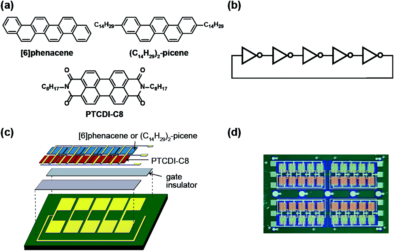 | ||
| Fig. 1 (a) Molecular structures of [6]phenacene, (C14H29)2-picene, and PTCDI-C8. (b) Equivalent circuit of ring oscillator. (c) Protocol for fabrication of the ring oscillator employed in this study. (d) Photograph of the ring oscillator fabricated in this study. Four sets of ring oscillators were formed. | ||
First, the electrodes were prepared on the SiO2/Si substrate, which become the gate electrodes for operating the FETs constituting each inverter. Next, a 600 nm-thick parylene or 320 nm-thick ZrO2 gate dielectric was formed on the electrodes. The parylene thin film was prepared according to the procedure described elsewhere,30 and the ZrO2 thin film was prepared by electron beam evaporation, as described previously.30 The gate dielectric was not formed in the central area to establish contacts between the output and input electrodes in each inverter. Subsequently, active layers were prepared by the thermal deposition of organic materials under a vacuum of 10−7 Torr for p-channel and n-channel FET operations; either [6]phenacene or (C14H29)2-picene was used for the p-channel active layer, while PTCDI-C8 was used for the n-channel active layer. The thickness of the active layer was 60 nm. Finally, the top electrodes were fabricated for voltage application (VDD), ground (GND), and detection of output voltage (Vout). All electrodes were formed by the thermal deposition of gold (Au) under a vacuum of 10−7 Torr, and the Au layer was 100 nm thick for the gate electrodes, and 150 nm for the top electrodes. Also, 5 nm-thick chromium (Cr) was inserted between the gate electrode and SiO2/Si substrate to increase the adhesion, while a 3 nm-thick 7,7,8,8-teracyano-quinodimethane was inserted between the active layer and top electrodes to reduce the contact resistance. A photograph of the ring oscillator prepared is shown in Fig. 1(d). In this study, the ring oscillators were prepared with active layers using (C14H29)2-picene and PTCDI-C8 FETs, as well as [6]phenacene and PTCDI-C8 FETs, where a parylene gate dielectric was used. Also, a ring oscillator was fabricated using [6]phenacene and PTCDI-C8 FETs, as well as a ZrO2 gate dielectric to reduce the operation voltage.
The channel length (L) of the [6]phenacene and PTCDI-C8 FETs contained in the ring oscillator was 200 μm, while the values of channel width (W) were 200 μm for the [6]phenacene FET and 500 μm for the PTCDI-C8 FETs in this ring oscillator, where parylene was used for the gate dielectric. The L value of the (C14H29)2-picene and PTCDI-C8 FETs in the ring oscillator was 300 μm, while the W values were 500 μm for the (C14H29)2-picene FET and 1000 μm for the PTCDI-C8 FETs in the ring oscillator, where parylene was used for the gate dielectric. The L of the [6]phenacene and PTCDI-C8 FETs in the ring oscillator was 300 μm, while the values of W were 500 μm for the [6]phenacene FET and 1000 μm for the PTCDI-C8 FETs in this ring oscillator, where ZrO2 was used for the gate dielectric.
The capacitance per area of the parylene gate dielectric, C0, was determined experimentally to be 4.57 nF cm−2 in the ring oscillator composed of [6]phenacene/PTCDI-C8 FETs, and 6.15 nF cm−2 in that composed of (C14H29)2-picene/PTCDI-C8 FETs. The C0 value for ZrO2 was experimentally determined to be 30.9 nF cm−2 in the ring oscillator composed of [6]phenacene/PTCDI-C8 FETs. These values were directly measured using the corresponding devices. The difference in C0 of the parylene film described above may be due to some microscopic quality of the film because its thickness was fixed at 600 nm. In fact, the FET parameters were precisely evaluated because the values of the real C0 were employed.
The operating properties of each FET device and inverter constituting the ring oscillator were measured in two-terminal measurement mode at room temperature. The operating properties were recorded using an Agilent B1500A semiconductor parametric analyzer in an Ar-filled glove box (O2 < 0.3 ppm, H2O < 3 ppm). The FET properties were analyzed with the following equation in the saturation regime:34
 | (1) |
 | ||
| Fig. 2 Measurement modes of (a) p-channel FET properties, (b) n-channel FET properties, (b) CMOS inverter, and (d) ring oscillator. Devices discussed in Sections 3.1 to 3.4 are shown. | ||
 | ||
| Fig. 3 Transfer (left) and output (right) characteristics of thin-film FETs with (a) [6]phenacene, (b) C14H29-picene and (c) PTCDI-C8. The device structure is bottom-gate top-contact type, and 300 nm-thick SiO2 was used for the gate dielectric. Two-terminal mode was used for the measurement of FET properties. | ||
3. Results and discussion
3.1. Characteristics of FET devices constituting a ring oscillator
The transfer and output curves of independent [6]phenacene, (C14H29)2-picene and PTCDI-C8 thin-film FETs are shown in Fig. 3(a)–(c); 400 nm-thick SiO2 was used for the gate dielectric. The transfer and output curves of both the [6]phenacene and (C14H29)2-picene thin-film FETs showed p-channel properties, which are the same as in previous reports.19,21,25,30 The values of μ and Vth were 1.1 cm2 V−1 s−1 and 26 V, for a [6]phenacene FET, and 4.0 cm2 V−1 s−1 and 51 V for a (C14H29)2-picene thin-film FET. On the other hand, the transfer and output curves of the PTCDI-C8 thin-film FETs showed n-channel properties, demonstrating the same behaviour as previous reports;30 the values of μ and Vth were 2.5 × 10⁻¹ cm2 V−1 s−1 and 44 V. Thus, these FETs displayed either p-channel or n-channel unipolar behaviour.Fig. 4(a) and (b) show the transfer and output characteristics of the [6]phenacene thin-film FET, which constitutes the p-channel part of one CMOS inverter in the ring oscillator; the n-channel part of the inverter is a PTCDI-C8 FET. The ring oscillator comprises five inverters, in which a 600 nm-thick parylene layer was used for the gate dielectric. The ring oscillator provides an fosc value of 26 Hz, which will be described later. The measurement mode of the FET characteristics is illustrated in Fig. 2(a). As shown in Fig. 4(a) and (b), p-channel FET characteristics were observed for the [6]phenacene FET, and weak n-channel FET properties were observed as well, indicating ambipolar properties. The characteristics of the [6]phenacene thin-film FET were affected by the PTCDI-C8 thin-film FET, which typically exhibits n-channel FET characteristics. Moreover, as shown in Fig. 4(c) and (d), the PTCDI-C8 thin-film FET showed not only n-channel FET characteristics, but also weak p-channel characteristics, i.e., weak ambipolar characteristics were observed as well, as in the [6]phenacene FET; the measurement mode is shown in Fig. 2(b). Ambipolar characteristics were observed because another FET was operating below the absolute threshold voltage |Vth| for each FET.
 | ||
| Fig. 4 (a) Transfer and (b) output characteristics of a [6]phenacene thin-film FET, which constitutes the p-channel part of the CMOS inverter in the ring oscillator (fosc = 26 Hz at VDD = 100 V). (c) Transfer and (d) output characteristics of a PTCDI-C8 thin-film FET, which constitutes the n-channel part of the CMOS inverter in the ring oscillator (fosc = 26 Hz at VDD = 100 V). In (a) and (c), the p-channel and n-channel parts are shown by orange and blue backgrounds, respectively. The gate dielectric was 600 nm-thick parylene. The FETs employed refer to device 3 (#3) in Table 1. | ||
Fig. 5(a) and (b) show the transfer and output characteristics of the (C14H29)2-picene thin-film FET, which constitutes the p-channel part of one CMOS inverter in the ring oscillator, providing an fosc value of 21 Hz. PTCDI-C8 was employed as the active layer of the n-channel part. The measurement mode of the FET characteristics is illustrated in Fig. 2(a). As shown in Fig. 5(a) and (b), p-channel FET characteristics were observed for the (C14H29)2-picene FET, together with clear n-channel FET characteristics, indicating ambipolar properties. Therefore, the operation of the (C14H29)2-picene thin-film FET was affected by the PTCDI-C8 thin-film FET. As shown in Fig. 5(c) and (d), the PTCDI-C8 thin-film FET showed not only n-channel FET characteristics, but also p-channel characteristics; the measurement mode is shown in Fig. 2(b). Therefore, the ambipolar FET characteristics in the (C14H29)2-picene/PTCDI-C8 inverter are clearer than those discovered in the CMOS inverter with [6]phenacene and PTCDI-C8. In addition, a small hysteresis was observed in the forward and reverse transfer curves (Fig. 4 and 5), which probably originates from the bias stress effect. Namely, the reverse curve degrades slightly owing to the formation of trap states induced by the bias voltage application. In particular, the characteristics due to the p-channel FET showed a larger hysteresis than those due to the n-channel FET, demonstrating a stronger bias stress effect. In addition, in the case of using an SiO2 gate dielectric treated with 1,1,1,3,3,3-hexamethyldisilazane (HMDS), the hysteresis of a picene thin-film FET may be larger than that of [6]phenacene and [7]phenacene thin-film FETs,9,19,20 although this may be due to an extrinsic factor such as the difference in hydrophobicity of the surface of gate dielectric.
 | ||
| Fig. 5 (a) Transfer and (b) output characteristics of a (C14H29)2-picene thin-film FET, which constitutes the p-channel part of the CMOS inverter in the ring oscillator (fosc = 21 Hz at VDD = 100 V). (c) Transfer and (d) output characteristics of a PTCDI-C8 thin-film FET, which constitutes the n-channel part of the CMOS inverter in the ring oscillator (fosc = 21 Hz at VDD = 100 V). In (a) and (c), the p-channel and n-channel parts are shown by orange and blue backgrounds, respectively. The gate dielectric was 600 nm-thick parylene. The FETs employed refer to device 1 (#1) in Table 2. | ||
Previous studies indicated that [6]phenacene and (C14H29)2-picene thin-film FETs exhibited only p-channel FET characteristics when these devices were not electrically connected to PTCDI-C8 FETs.19,21,25,30 Meanwhile, only n-channel FET characteristics should be observed in PTCDI-C8 thin-film FET devices separated electrically from a p-channel FET, as reported previously.30,35
The FET parameters of the [6]phenacene and PTCDI-C8 thin-film FETs in the inverters constituting the ring oscillator (fosc = 26 Hz) fabricated in this study are listed in Table 1. The average values of μ and Vth (<μ> and <Vth>) were 8(4) × 10−1 cm2 V−1 s−1 and −2(3) × 10 V for the [6]phenacene thin-film FET, respectively. Because of the ambipolar FET properties, the <μ> and <Vth> were a little subpar, i.e., low μ and high <|Vth|> were obtained, in comparison with those recorded for the normal [6]phenacene thin-film FET without electrical series connection with an n-channel FET device.19,21 In particular, the average on–off ratio (<on–off ratio>) was exactly low, as shown in Table 1.
| [6]Phenacene | PTCDI-C8 | ||||||||
|---|---|---|---|---|---|---|---|---|---|
| Device | Μ (cm2 V−1 s−1) | Vth (V) | On–off | S (V per decade) | Device | Μ (cm2 V−1 s−1) | Vth (V) | On–off | S (V per decade) |
| #1 | 8.1 × 10⁻¹ | −7.0 × 101 | 2.69 ×10³ | 2.7 × 101 | #1 | 2.33 × 10⁻¹ | 8.7 | 4.8 × 101 | 1.0 × 101 |
| #2 | 8.1 × 10⁻¹ | −3.1 × 101 | 2.71 | 8.2 × 101 | #2 | 1.69 × 10⁻¹ | −1.5 | 3.2 | 9.7 × 101 |
| #3 | 1.19 | −1.1 × 101 | 6.12 | 6.1 × 101 | #3 | 1.50 × 10⁻¹ | −7.7 | 3.1 | 9.9 × 101 |
| #4 | 2.7 × 10⁻¹ | 1.7 × 101 | 2.44 | 1.2 × 10² | #4 | 1.96 × 10⁻¹ | 6.1 | 4.8 | 8.0 × 101 |
| #5 | 1.16 | −1.4 × 101 | 5.71 | 5.9 × 101 | #5 | 2.27 × 10⁻¹ | 9.9 | 4.7 | 8.0 × 101 |
| Average | 8(4) × 10−1 | −2(3) × 101 | 5(12) × 102 | 7(4) × 101 | Average | 2.0(4) × 10−1 | 3(7) | 1(2) × 101 | 8(3) × 101 |
In addition, studies on overestimation of the μ value have recently been reported.36,37 One of the studies recommended showing the measurement reliability factor (rsat) for the evaluated mobility values.37 The values of rsat for [6]phenacene and (C14H29)2-picene thin-film FETs with SiO2 gate dielectrics showing high μ values of 7.4 and 3.9 cm2 V−1 s−1, which were reported previously,21,25 were found to be 9.3% and 24% in this study, respectively, indicating effective mobilities, μeff (=rsat × μ), of 0.69 and 0.94 cm2 V−1 s−1. On the other hand, the value of rsat was 27% for a (C14H29)2-picene thin-film FET with ZrO2 gate dielectric showing the μ value of 5.1 cm2 V−1 s−1,30 demonstrating an effective mobility value of 1.3 cm2 V−1 s−1. Here, the rsat value was determined using the formula reported in ref. 37. In this study, no further investigation of the effective mobility was made for the FETs constituting the ring oscillator. Therefore, in this paper, the FET properties will be discussed based on the value of μ (not effective mobility), but it may be necessary to consider the effective mobility if high FET performance is reported.
The high subthreshold slope (<S>) was due to the ambipolar properties. The values of <μ> and <Vth> were 2.0(4) × 10−1 cm2 V−1 s−1 and 3(7) V for the PTCDI-C8 thin-film FET; the μ value was much lower than that in the FET using a PTCDI-C8 thin film formed on pentacene, as reported recently.35 The values of <on–off ratio> and <S> were subpar because of the ambipolar properties observed in a series connection of CMOS inverters composed of p-channel and n-channel FETs. To summarize, the relatively low FET properties recorded in this study were not due to the intrinsic nature of the materials employed, but the electrical series connections of the inverters.
All FET parameters in the (C14H29)2-picene thin-film and PTCDI-C8 thin-film FETs in the CMOS inverters constituting the ring oscillator (fosc = 21 Hz) fabricated in this study are listed in Table 2. The average values of μ and Vth (<μ> and <Vth>) were 1.4(7) cm2 V−1 s−1 and −5.9(9) × 10 V for the (C14H29)2-picene thin-film FET. The <μ> value for the normal (C14H29)2-picene thin-film FET recorded previously by our group was beyond 5 cm2 V−1 s−1.25 The low <on–off ratio> and high <S> were due to the ambipolar properties observed in the series connection of CMOS inverters. The values of <μ> and <Vth> were respectively 1.3(5) × 10−1 cm2 V−1 s−1 and 9.2(6) V for the PTCDI-C8 thin-film FET. Similarly, the low value of <on–off ratio> and high <S> were likely due to the effects of the ambipolar properties observed in the series connection of CMOS inverters.
| (C14H29)2-Picene | PTCDI-C8 | ||||||||
|---|---|---|---|---|---|---|---|---|---|
| Device | Μ (cm2 V−1 s−1) | Vth (V) | On–off | S (V per decade) | Device | μ (cm2 V−1 s−1) | Vth (V) | On–off | S (V per decade) |
| #1 | 1.85 | −6.0 × 101 | 6.6 | 3.60 × 101 | #1 | 1.54 × 10⁻¹ | 9.49 | 1.03 × 101 | 5.13 × 101 |
| #2 | 2.40 × 10⁻¹ | −4.4 × 101 | 6.8 | 5.24 × 101 | #2 | 3.10 × 10⁻² | 9.74 | 8.29 | 4.92 × 101 |
| #3 | 1.73 | −6.3 × 101 | 9.8 | 2.99 × 101 | #3 | 1.53 × 10⁻¹ | 8.51 | 1.82 × 101 | 5.08 × 101 |
| #4 | 1.90 | −6.4 × 101 | 7.0 | 3.37 × 101 | #4 | 1.53 × 10⁻¹ | 9.39 | 1.21 × 101 | 5.00 × 101 |
| #5 | 1.19 | −6.6 × 101 | 5.4 | 3.13 × 101 | #5 | 1.52 × 10⁻¹ | 8.60 | 1.30 × 101 | 4.66 × 101 |
| Average | 1.4(7) | −5.9(9) × 101 | 7(2) | 3.7(9) × 101 | Average | 1.3(5) × 10−1 | 9.2(6) | 1.2(4) × 101 | 5.0(2) × 101 |
3.2. Characteristics of CMOS inverters in the ring oscillators
Fig. 6(a) shows plots of Vout–Vin (inverter characteristics) and |dVout/dVin|–Vin (gain plot) for one CMOS inverter based on [6]phenacene and PTCDI-C8 thin-film FETs, which form a ring oscillator with an fosc of 26 Hz. The inverter contains the [6]phenacene and PTCDI-C8 thin-film FETs described in Section 3.1. Clear inverter properties were observed in the plot shown in Fig. 6(a); the method used to measure the inverter properties is shown in Fig. 2(c). The VDD was 100 V. As shown in Fig. 6(a), the Vin (59.7 V for the forward measurement and 47.5 V for the reverse measurement) providing half the maximum value of Vout (called “logic threshold voltage (VTC)”) deviates slightly from the ideal value of VDD/2 = 50 V. The gain plot of the CMOS inverter with [6]phenacene and PTCDI-C8 thin-film FETs is shown in Fig. 6(a), which was obtained from the first derivative of the Vout–Vin plot (Fig. 6(a)). The gain of the CMOS inverter above was evaluated to be 285.8 for the forward measurement and 145.3 for the reverse measurement, which is slightly lower than that (∼300) of recent CMOS inverters formed on a plastic substrate using [6]phenacene and PTCDI-C8 thin-film FETs.30 It is worth noting that the inverter properties were measured using a fabricated ring oscillator, i.e., five inverters were connected in series (Fig. 2(d)). Therefore, these inverter properties cannot be compared directly with the previous inverter properties. | ||
| Fig. 6 Plots of Vout–Vin and dVout/dVin–Vin in (a) a CMOS inverter composed of [6]phenacene and PTCDI-C8 FETs, which is a block of ring oscillators (fosc = 26 Hz at VDD = 100 V), and (b) a CMOS inverter composed of (C14H29)2-picene and PTCDI-C8 FETs FET, which is a block of ring oscillators (fosc = 21 Hz at VDD = 100 V). The gate dielectric was 600 nm-thick parylene. The blue and red curves refer to the plots recorded in forward and reverse measurement modes, respectively (see text). The inverter in (a) corresponds to Device 3 (#3) in Table 3, while the inverter in (b) corresponds to Device 1 (#1) in Table 4. | ||
The VTC value of the CMOS inverter circuit is given by the following equation:38
 | (2) |
 ; kp and kn refer to the k values for the p- and n-channel FETs; VTHp and VTHn refer to the VTH values for the p- and n-channel FETs. By substituting the FET parameters obtained in Section 3.1 into eqn (2), we evaluated the VTC for the CMOS inverter above and obtained a value of 54.2 V. This VTC value is consistent with the average (<VTC> = 53.6 V) of the values observed in the forward and reverse measurements (VTC = 59.7 V and VTC = 47.5 V), which indicates the effectiveness of the above equation and the reliability of the FET parameters in Section 3.1. The values of gain and VTC for all inverters constituting the ring oscillator are listed in Table 3; the plots shown in Fig. 6(a) were obtained using the inverter device (#3) in Table 3.
| Device | Forward | Reverse | ||
|---|---|---|---|---|
| VTC (V) | Gain | VTC (V) | Gain | |
| #1 | 55.9 | 32.9 | 52.4 | 25.2 |
| #2 | 37.7 | 67.8 | 33.0 | 193.4 |
| #3 | 59.7 | 285.8 | 47.5 | 145.3 |
| #4 | 58.2 | 181.4 | 48.3 | 262.4 |
| #5 | 54.9 | 146.6 | 50.5 | 60.9 |
| Average | 53(9) | 143(100) | 46(8) | 140(97) |
Fig. 6(b) shows plots of Vout–Vin and |dVout/dVin|–Vin for one CMOS inverter built with (C14H29)2-picene and PTCDI-C8 thin-film FETs, which created a ring oscillator with an fosc of 21 Hz. The inverter was composed of the (C14H29)2-picene and PTCDI-C8 thin-film FETs evaluated in Section 3.1. Clear inverter properties were observed in the Vout–Vin plot shown in Fig. 6(b); the VDD was 100 V. As shown in Fig. 6(b), the observed value of VTC (38.9 V for the forward measurement and 33.9 V for the reverse measurement) deviated from the value of VDD/2 = 50 V. The gain plot obtained from the first derivative of the Vout–Vin plot (Fig. 6(b)) for the CMOS inverter with (C14H29)2-picene and PTCDI-C8 thin-film FETs is shown in Fig. 6(b). The gain of the above CMOS inverter was evaluated to be 61.8 for the forward measurement and 90.8 for the reverse measurement. As described above, the five inverters were connected in series in the measurement of the inverter properties, which may suppress the gain of each inverter. Using eqn (2), we evaluated the theoretical value of VTC for the CMOS inverter and obtained a value of 31.2 V. This VTC value is almost consistent with the <VTC> (=36.4 V) obtained from VTC = 38.9 V (forward measurement) and VTC = 33.9 V (reverse measurement), which also indicates the effectiveness of the above equation and the reliability of the FET parameters in Section 3.1. The values of gain and VTC for all inverters constituting the ring oscillator are listed in Table 4; the plots shown in Fig. 6(b) are obtained using Inverter Device 1 (#1). We note that significant hysteresis in the Vout–Vin plots (Fig. 6(a) and (b)) is observed owing to the bias stress effect found in p-channel FETs as described in Section 3.1. The bias stress effect is discussed later in detail.
| Device | Forward | Reverse | ||
|---|---|---|---|---|
| VTC (V) | Gain | VTC (V) | Gain | |
| #1 | 38.9 | 61.8 | 33.9 | 90.8 |
| #2 | 38.8 | 54.1 | 33.5 | 108.7 |
| #3 | 41.1 | 50.9 | 33.8 | 159.6 |
| #4 | 38.6 | 56.5 | 33.5 | 281.3 |
| #5 | 36.6 | 47.1 | 30.9 | 125.5 |
| Average | 39(2) | 54(6) | 33(1) | 153(76) |
3.3. Ring oscillators using CMOS inverters composed of phenacene and PTCDI-C8 FETs
Fig. 7(a) shows the Vout–t plot for the ring oscillator comprising five CMOS inverters. Each inverter was fabricated using a [6]phenacene thin-film FET for p-channel operation and a PTCDI-C8 thin-film FET for n-channel operation. Furthermore, a 600 nm-thick parylene film was used for the gate dielectric in the ring oscillator. As shown in Fig. 7(a), the value of the operation frequency, fosc was 26 Hz when VDD was 100 V. This is the first time acceptable operation of a ring oscillator using phenacene molecules, although the fosc value of 1 Hz has been recorded previously in a ring oscillator using [6]phenacene and PTCDI-C8.33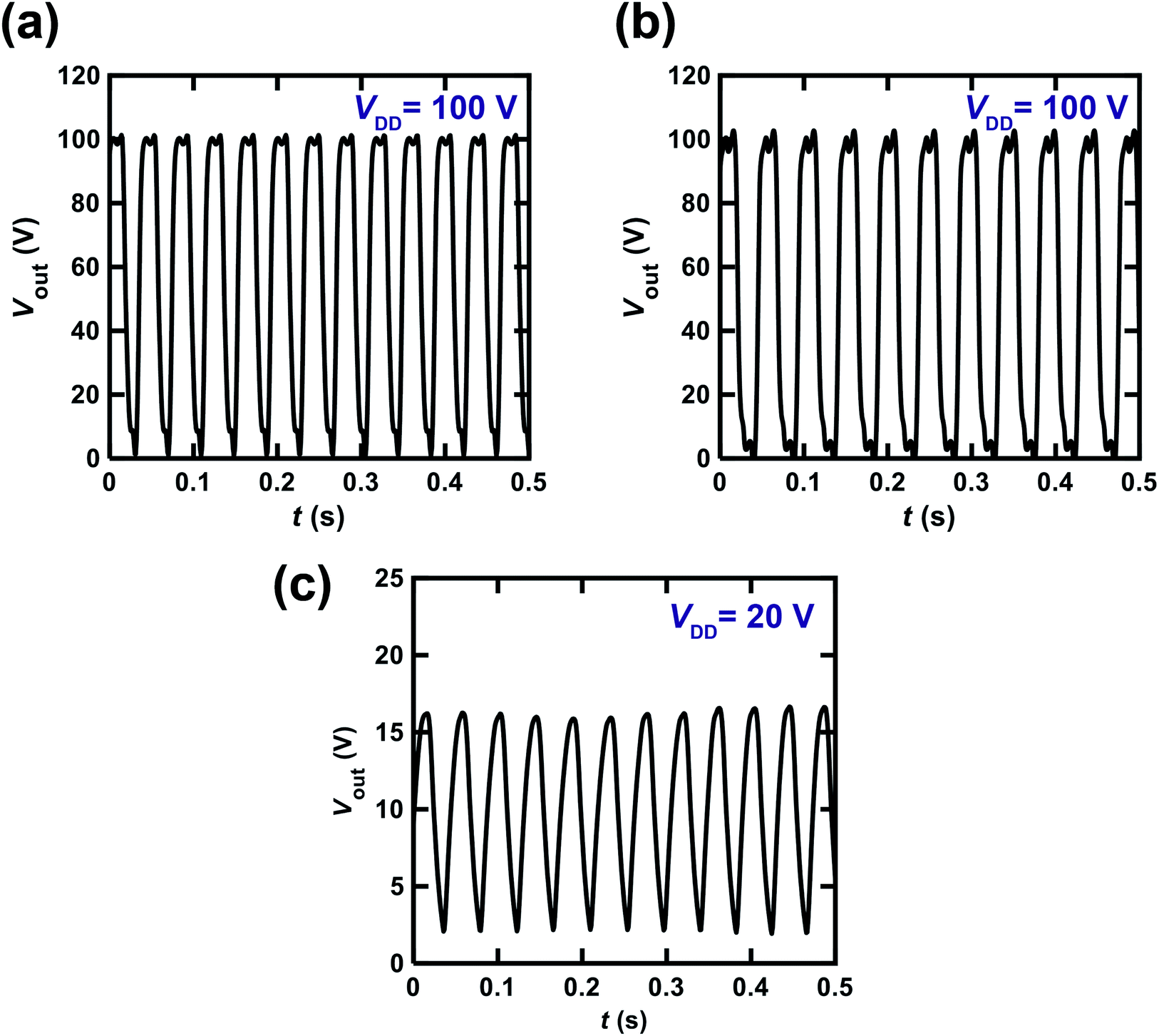 | ||
| Fig. 7 Vout–t plots of ring oscillators comprising five inverters, composed of (a) [6]phenacene and PTCDI-C8 thin-film FETs, and (b) (C14H29)2-picene and PTCDI-C8 FETs. In (a) and (b), the gate dielectric was 600 nm-thick parylene. (c) Vout–t plot of a ring oscillator comprising five inverters, composed of [6]phenacene and PTCDI-C8 thin-film FETs; the gate dielectric was 320 nm-thick ZrO2. | ||
Fig. 7(b) shows the Vout–t plot for a ring oscillator comprising five CMOS inverters; each inverter was fabricated using a (C14H29)2-picene thin-film FET for p-channel operation and a PTCDI-C8 thin-film FET for n-channel operation. Furthermore, a 600 nm-thick parylene film was used for the gate dielectric in this ring oscillator. As shown in Fig. 7(b), the value of fosc was 21 Hz when a VDD of 100 V was applied. Therefore, the clear operation of the ring oscillator was confirmed when using [6]phenacene/PTCDI-C8 FETs and (C14H29)2-picene/PTCDI-C8 FETs, indicating the possibility of using the above FETs in RFID devices.
We also attempted to fabricate a ring oscillator incorporating five inverters composed of [6]phenacene/PTCDI-C8 FETs with a ZrO2 gate dielectric to realize low-voltage operation. The Vout–t plot of the ring oscillator is shown in Fig. 7(c). A VDD of 20 V was applied to this ring oscillator, providing a 24 Hz oscillation. This device performance is comparable to those of the ring oscillators above using parylene gate dielectrics. Therefore, low-voltage operation was realized using a ZrO2 gate dielectric, as described below.
We changed the VDD value applied to the ring oscillator to verify the operation properties. Fig. 8 shows the Vout–t plots for the ring oscillator composed of five inverters using [6]phenacene and PTCDI-C8 FETs with the parylene gate dielectric measured at different VDD. When VDD was decreased from 120 to 40 V, the fosc and the amplitude of Vout decreased gradually, so the fosc was 28 Hz for VDD = 120 V, and 10 Hz for VDD = 80 V. Below VDD = 40 V, oscillations were not observed. Thus it was found that the threshold VDD for oscillation was 40 V for this ring oscillator.
 | ||
| Fig. 8 Vout–t plots of ring oscillators comprising five inverters, which are composed of [6]phenacene and PTCDI-C8 thin-film FETs, measured at different VDD values. The gate dielectric was 600 nm-thick parylene. | ||
Fig. 9 shows the Vout–t plots for the ring oscillator composed of five inverters using [6]phenacene and PTCDI-C8 FETs with ZrO2 gate dielectrics, as measured at different VDD. When decreasing VDD from 22 to 8 V, the fosc decreased gradually. Specifically, the fosc was 25 Hz for VDD = 22 V and 8.8 Hz for VDD = 14 V. Below VDD = 8 V, oscillations were not observed. Thus, the threshold VDD for the oscillation of this ring oscillator was 8 V, showing the operation of a ring oscillator at a lower voltage than that (threshold VDD of 40 V) of the previous ring oscillator (Fig. 8). Namely, the ZrO2 gate dielectric used in the ring oscillator resulted in low-voltage operation. In addition, as shown in Fig. 8, the amplitude of Vout increased when VDD was decreased from 22 to 18 V and then decreased when VDD was further decreased. The origin of the increase is still unclear.
 | ||
| Fig. 9 Vout–t plots of ring oscillators comprising five inverters, which are composed of [6]phenacene and PTCDI-C8 thin-film FETs, measured at different VDD values. The gate dielectric was 320 nm-thick ZrO2. | ||
The fosc value of the ring oscillator obtained in this study is smaller than that (=200 kHz) of the ring oscillator composed of five CMOS inverters with pentacene/C60 FETs,39 which is a small-sized device where L = 2 μm. The ring oscillator was fabricated by the mass-printed roll-to-roll method, where five unipolar inverters with a conjugated polymer, poly[[2,2′-bithiophene]-5,5′-diyl(9,9-dioctyl-9H-fluorene-2,7-diyl)] (F8T2), was utilized and provided an fosc of 6 Hz; the L was 100 μm, which was the same order as those (L = 200 or 300 μm) of the ring oscillators in this study.40 The fosc value was smaller than that of our ring oscillator (∼26 Hz). It is shown in ref. 41 that fosc is clearly correlated with L. A smaller L in the FET blocks in each inverter of the ring oscillator provides a higher fosc. This result is explained by the theoretical model described below.33,38
The fosc value is expressed as follows:
 | (3) |
τp is expressed by
| τp = (τpLH + τpHL)/2. | (4) |
 | (5) |
 | (6) |
 , where kp and kn refer to the k values for the p- and n-channel FETs, as described in Section 3.2. As shown in eqn (3), a decrease in n results in an increase in fosc. In addition, the values of experimental <τp> were determined to be 3.8 ms for fosc = 26 Hz (Fig. 7(a)) and 4.8 ms for fosc = 21 Hz (Fig. 7(b)) from the equation,
  .
.
As shown in eqn (4)–(6), a smaller L should provide a smaller <τp> through a larger kp and kn. Consequently, a smaller <τp> results in a larger fosc, as indicated from eqn (3). It is noteworthy that a larger W (=500 or 1000 μm) in the PTCDI-C8 thin-film FET than that (W = 200 or 300 μm) in the p-channel FET was used in the ring oscillator, so that the small μ value obtained in the n-channel PTCDI-C8 FET was compensated in  . To summarize, the fabrication of a ring oscillator with a smaller L (i.e., a microscale ring oscillator) will significantly increase the value of fosc. Furthermore, a larger value of μ must be realized in n-channel FETs, because the inferior μ value of an n-channel FET should enhance <τp> to reduce the value of fosc. In the future, the solution to these problems will be attempted in the fabrication of practical RFIDs using phenacene molecules.
The decent operation of a ring oscillator via a combination of phenacene molecules and PTCDI-C8 is an important step for the integration of practical organic logic gate circuits, regardless of the observed low oscillation frequency, because the phenacene molecules provide high FET performance. In addition, the diverse possibilities and the ease with which phenacene molecules can be designed appears quite likely to lead to the development of promising materials for ring oscillators with high oscillation frequency in the near future. Finally, we comment briefly on a relevant recent ring oscillator based on a small organic molecule, 2,9-diphenyl-dinaphtho-[2,3-b:2′,3′-f]thieno[3,2-b]thiophene (DPh-DNTT).42 The best value of τp was 138 ns for the ring oscillator. Our next research target is to fabricate a ring oscillator with a τp comparable to that value using phenacene molecules. For this purpose, we will optimize the device structure, as well as searching for more suitable phenacene molecules for the ring oscillator. Also, to fabricate ring oscillators using phenacene molecules on a plastic or glass substrate, which may have a smaller parasitic capacitance than an SiO2/Si substrate, would be a future task to realize a ring oscillator with a high value of fosc.
3.4. Durability of ring oscillators fabricated using phenacene and PTCDI-C8 FETs
Fig. 10(a) shows the Vout–t plot for the ring oscillator comprising five CMOS inverters; each inverter was fabricated using a [6]phenacene thin-film FET for p-channel operation and a PTCDI-C8 thin-film FET for n-channel operation; the parylene film was used for the gate dielectric in this ring oscillator. As shown in Fig. 10(a), the fosc was 26 Hz when the applied VDD was 100 V. The ring oscillator was operated continuously for 2 h, and then the Vout–t plot was recorded (Fig. 10(b)), indicating a 16 Hz operation in the ring oscillator. Namely, the value of fosc decreased from 26 to 16 Hz during continuous application of VDD = 100 V. Furthermore, the amplitude of Vout decreased from 100 (Fig. 10(a)) to 50 V (Fig. 10(b)). Thus both the fosc and amplitude of Vout were decreased by continuous operation of the ring oscillator, which was likely due to the bias stress effect. The bias stress effect degraded the FET properties in the phenacene thin-film FET,16,19,26,30 which may have been caused by the presence of trap states in the interface between the phenacene/PTCDI-C8 and the parylene gate dielectric. The trap states were produced by a trace of water at the interface and gate voltage application.43–48 The small amount of water at the interface, which yields trap states, might not be removed for a long time, even in an Ar-filled glove box, which is a common phenomenon. | ||
| Fig. 10 Vout–t plots of ring oscillators using five inverters that are composed of [6]phenacene and PTCDI-C8 thin-film FETs and a gate dielectric of 600 nm-thick parylene. Vout–t plots recorded at (a) the first measurement and (b) the measurement after a continuous application of VDD = 100 V for 2 h. (c) Plots of Vmax and Vmin as a function of t of the ring oscillator, which refer to the variation in Vout measured between the plots shown in (a) and (b). (d) Vout–t plot measured after storing the ring oscillator device above without applying VDD for two months. | ||
Fig. 10(c) shows the Vmax–t and Vmin–t plots for the ring oscillator, indicating that the value of Vmax minus Vmin (amplitude of Vout) decreases continuously above t = 30 min. In other words, the amplitude of Vout remains constant up to ∼30 min. We stopped the operation of the ring oscillator and stored the ring oscillator without any VDD for two months. After two months, we recorded the Vout–t plot (Fig. 10(d)), which showed an fosc value of 19 Hz, and an Vout amplitude of 90 V. Therefore, the oscillation performance was recovered by not applying VDD for two months. The features are intrinsically the same as the bias-stress degradation of FET properties discovered in some phenacene thin-film FETs.16,19,26,30
4. Conclusion
In this study, the successful operation of a ring oscillator composed of five CMOS inverters using phenacene and PTCDI-C8 thin-film FETs was demonstrated. An fosc value exceeding 20 Hz was stably observed using a [6]phenacene or (C14H29)2-picene thin-film FET for p-channel operation and a PTCDI-C8 thin-film FET for n-channel operation. A parylene gate dielectric was used for the ring oscillator. Moreover, the ring oscillator using CMOS inverters composed of [6]phenacene and PTCDI-C8 FETs with ZrO2 showed a low-voltage operation. The value of fosc obtained was the same as that using the parylene gate dielectric. The durability experiment on the ring oscillator clarified the presence of the bias stress effect in the ring oscillator, i.e., the fosc and Vout amplitude decreased significantly. However, the performance of the ring oscillator was restored by storing the device without applying a VDD for two months. The successful operation of the ring oscillator demonstrated the potential application of phenacene molecules in integrated logic gate circuits, and a workable fabrication process for the ring oscillator was shown clearly in this study. Therefore, this is of significance as the initial stage of the development of high-performance integrated logic gate circuits using phenacene molecules, even if the oscillation frequency is still low. Thus, this study can serve as a basis for the fabrication of RFIDs using phenacene molecules.Author contribution
All the authors contributed to the writing of this manuscript. All authors have given their approval to the final version of the manuscript.Conflicts of interest
There are no conflicts to declare.Acknowledgements
This study was partly supported by Grants-in-aid (17K05976, 18K18736 and 19H02676, 20K05648, 20H05878, and 20H05879) from MEXT, and the MEXT Program for Promoting the Enhancement of Research Universities, and Okayama Foundation for Science and Technology.References
- Y.-Y. Lin, D. J. Gundlach, S. F. Nelson and T. N. Jackson, IEEE Electron Device Lett., 1997, 12, 606–608 Search PubMed.
- R. C. Haddon, A. S. Perel, R. C. Morris, T. T. M. Palstra, A. F. Hebard and R. M. Fleming, Appl. Phys. Lett., 1995, 67, 121 CrossRef CAS.
- T. B. Singh, N. Marjanovic, G. J. Matt, S. Günes, N. S. Sariciftci, A. M. Ramil, A. Andreev, H. Sitter, R. Schwödiauer and S. Bauer, Org. Electron., 2005, 6, 105–110 CrossRef CAS.
- T. D. Anthopoulos, B. Singh, N. Marjanovic, N. S. Sariciftci, A. M. Ramil, H. Sitter, M. Cölle and M. de Leeuw, Appl. Phys. Lett., 2006, 89, 213504 CrossRef.
- J. Takeya, M. Yamagishi, Y. Tominari, R. Hirahara, Y. Nakazawa, T. Nishikawa, T. Kawase, T. Shimoda and S. Ogawa, Appl. Phys. Lett., 2007, 90, 102120 CrossRef.
- J. Soeda, Y. Hirose, M. Yamagishi, A. Nakao, T. Uemura, K. Nakayama, M. Uno, Y. Nakazawa, K. Takimiya and J. Takeya, Adv. Mater., 2011, 23, 3309–3314 CrossRef CAS.
- N. Kurihara, A. Yao, M. Sunagawa, Y. Ikeda, K. Terai, H. Kondo, M. Saito, H. Ikeda and H. Nakamura, Jpn. J. Appl. Phys., 2013, 52, 05DC11 CrossRef.
- Y. Yuan, G. Giri, A. L. Ayzner, A. P. Zoombelt, S. C. B. Mannsfeld, J. Chen, D. Nordlund, M. F. Toney, J. Huang and Z. Bao, Nat. Commun., 2014, 5, 3005 CrossRef.
- H. Okamoto, N. Kawasaki, Y. Kaji, Y. Kubozono, A. Fujiwara and M. Yamaji, J. Am. Chem. Soc., 2008, 130, 10470–10471 CrossRef CAS.
- N. Kawasaki, Y. Kubozono, H. Okamoto, A. Fujiwara and M. Yamaji, Appl. Phys. Lett., 2009, 94, 043310 CrossRef.
- Y. Kaji, R. Mitsuhashi, X. Lee, H. Okamoto, T. Kambe, N. Ikeda, A. Fujiwara, M. Yamaji, K. Omote and Y. Kubozono, Org. Electron., 2009, 10, 432–436 CrossRef CAS.
- Y. Kaji, N. Kawasaki, X. Lee, H. Okamoto, Y. Sugawara, S. Oikawa, A. Ito, H. Okazaki, T. Yokoya, A. Fujiwara and Y. Kubozono, Appl. Phys. Lett., 2009, 95, 183302 CrossRef.
- N. Kawasaki, W. L. Kalb, T. Mathis, Y. Kaji, R. Mitsuhashi, H. Omote, Y. Sugawara, A. Fujiwara, Y. Kubozono and B. Batlogg, Appl. Phys. Lett., 2010, 96, 113305 CrossRef.
- X. Lee, Y. Sugawara, A. Ito, S. Oikawa, N. Kawasaki, Y. Kaji, R. Mitsuhashi, H. Okamoto, A. Fujiwara, K. Omote, T. Kambe, N. Ikeda and Y. Kubozono, Org. Electron., 2010, 11, 1394–1398 CrossRef CAS.
- Y. Kaji, K. Ogawa, R. Eguchi, H. Goto, Y. Sugawara, T. Kambe, K. Akaike, S. Gohda, A. Fujiwara and Y. Kubozono, Org. Electron., 2011, 12, 2076–2083 CrossRef CAS.
- Y. Sugawara, K. Ogawa, H. Goto, S. Oikawa, K. Akaike, N. Komura, R. Eguchi, Y. Kaji, S. Gohda and Y. Kubozono, Sens. Actuators, B, 2012, 171–172, 544–549 CrossRef CAS.
- S. Gottardi, T. Toccoli, S. Iannotta, P. Bettotti, A. Cassinese, M. Barra, L. Ricciotti and Y. Kubozono, J. Phys. Chem. C, 2012, 116, 24503–24511 CrossRef CAS.
- N. Kawai, R. Eguchi, H. Goto, K. Akaike, Y. Kaji, T. Kambe, A. Fujiwara and Y. Kubozono, J. Phys. Chem. C, 2012, 116, 7983–7988 CrossRef CAS.
- N. Komura, H. Goto, X. He, H. Mitamura, R. Eguchi, Y. Kaji, H. Okamoto, Y. Sugawara, S. Gohda, K. Sato and Y. Kubozono, Appl. Phys. Lett., 2012, 101, 083301 CrossRef.
- Y. Sugawara, Y. Kaji, K. Ogawa, R. Eguchi, S. Oikawa, H. Gohda, A. Fujiwara and Y. Kubozono, Appl. Phys. Lett., 2011, 98, 013303 CrossRef.
- R. Eguchi, X. He, S. Hamao, H. Goto, H. Okamoto, S. Gohda, K. Sato and Y. Kubozono, Phys. Chem. Chem. Phys., 2013, 15, 20611–20617 RSC.
- X. He, R. Eguchi, H. Goto, E. Uesugi, S. Hamao, Y. Takabayashi and Y. Kubozono, Org. Electron., 2013, 14, 1673–1682 CrossRef CAS.
- X. He, S. Hamao, R. Eguchi, H. Goto, Y. Yoshida, G. Saito and Y. Kubozono, J. Phys. Chem. C, 2014, 118, 5284–5293 CrossRef CAS.
- H. Okamoto, R. Eguchi, S. Hamao, H. Goto, K. Gotoh, Y. Sakai, M. Izumi, Y. Takaguchi, S. Gohda and Y. Kubozono, Sci. Rep., 2014, 4, 5330 CrossRef CAS.
- H. Okamoto, S. Hamao, H. Goto, Y. Sakai, M. Izumi, S. Gohda, Y. Kubozono and R. Eguchi, Sci. Rep., 2014, 4, 5048 CrossRef CAS.
- Y. Kubozono, X. He, S. Hamao, K. Teranishi, H. Goto, R. Eguchi, T. Kambe, S. Gohda and Y. Nishihara, Eur. J. Inorg. Chem., 2014, 3806–3819 CrossRef CAS.
- Y. Shimo, T. Mikami, H. T. Murakami, S. Hamao, H. Goto, H. Okamoto, S. Gohda, K. Sato, A. Cassinese, Y. Hayashi and Y. Kubozono, J. Mater. Chem. C, 2015, 3, 7370–7378 RSC.
- Y. Shimo, T. Mikami, S. Hamao, H. Goto, H. Okamoto, R. Eguchi, S. Gohda, Y. Hayashi and Y. Kubozono, Sci. Rep., 2016, 6, 21008 CrossRef CAS.
- H. Okamoto, S. Hamao, R. Eguchi, H. Goto, Y. Takabayashi, P. Y.-H. Yen, L. U. Liang, C.-W. Chou, G. Hoffmann, S. Gohda, H. Sugino, Y.-F. Liao, H. Ishii and Y. Kubozono, Sci. Rep., 2019, 9, 4009 CrossRef.
- E. Pompei, C. Turchetti, S. Hamao, A. Miura, H. Goto, H. Okamoto, A. Fujiwara, R. Eguchi and Y. Kubozono, J. Mater. Chem. C, 2019, 7, 6022–6033 RSC.
- A. A. Ruzaiqi, H. Okamoto, Y. Kubozono, U. Zschieschang, H. Klauk, P. Baran and H. Gleskova, Org. Electron., 2019, 73, 286–291 CrossRef.
- V. C. Sundar, J. Zaumseil, V. Podzorov, E. Menard, R. L. Willett, T. Someya, M. E. Gershenson and J. A. Rogers, Science, 2004, 303, 1644–1646 CrossRef CAS.
- Y. Kubozono, S. Hamao, T. Mikami, Y. Shimo, Y. Hayashi and H. Okamoto, Transistor application and intercalation chemistry of π-conjugated hydrocarbon molecules in Physics and chemistry of carbon-based materials: basics and applications, ed. Y. Kubozono, Springer, Singapore, 2019, pp. 229–252 Search PubMed.
- S. M. Sze, Semiconductor devices, physics and technology, John Willey & Sons, Inc, United States, 2002 Search PubMed.
- Z. Hu, Z. Lin, J. Su, J. Zhang, Y. Hao, J. Chang and J. Wu, ACS Appl. Electron. Mater., 2019, 1, 2030–2036 CrossRef CAS.
- E. G. Bittle, J. I. Basham, T. N. Jackson, O. D. Jurchescu and D. J. Gundlach, Nat. Commun., 2016, 7, 10908 CrossRef CAS.
- H. H. Choi, K. Cho, C. D. Frisbie, H. Sirringhaus and V. Podzorov, Nat. Mater., 2018, 17, 2–7 CrossRef CAS.
- S.-M. Kang and Y. Leblebici, CMOS digital integrated circuits, analysis and design, McGraw-Hill, Boston, 2003 Search PubMed.
- M. Kitamura, Y. Kuzumoto, S. Aomori and Y. Arakawa, Appl. Phys. Express, 2011, 4, 051601 CrossRef.
- A. C. Hübler, G. C. Schmidt, H. Kempa, K. Reuter, M. Hambsch and M. Bellmann, Org. Electron., 2011, 12, 419–423 CrossRef.
- C. P. Watson, B. A. Brown, J. Carter, J. Morgan and D. M. Taylor, Adv. Electron. Mater., 2016, 2, 1500322 CrossRef.
- J. W. Borchert, B. Peng, F. Letzkus, J. N. Burghartz, P. K. L. Chan, K. Zojer, S. Ludwigs and H. Klauk, Nat. Commun., 2019, 10, 1119 CrossRef.
- D. V. Lang, X. Chi, T. Siegrist, A. M. Sergent and A. P. Ramirez, Phys. Rev. Lett., 2004, 93, 076601 CrossRef CAS.
- H. L. Gomes, P. Stallinga, M. Cölle, D. M. de Leeuw and F. Biscarini, Appl. Phys. Lett., 2006, 88, 082101 CrossRef.
- C. Goldmann, D. J. Gundlach and B. Batlogg, Appl. Phys. Lett., 2006, 88, 063501 CrossRef.
- C. Goldmann, C. Krellner, K. P. Pernstich, S. Haas, D. J. Gundlach and B. Batlogg, J. Appl. Phys., 2006, 99, 034507 CrossRef.
- K. P. Pernstich, D. Oberhoff, C. Goldmann and B. Batlogg, Appl. Phys. Lett., 2006, 89, 213509 CrossRef.
- W. L. Kalb, T. Mathis, S. Haas, A. F. Strassen and B. Batlogg, Appl. Phys. Lett., 2007, 90, 092104 CrossRef.
| This journal is © The Royal Society of Chemistry 2021 |