DOI:
10.1039/D0RA10894D
(Paper)
RSC Adv., 2021,
11, 31159-31173
The effect of the metal and selenium precursors on the properties of NbSe2 and Nb2Se9 nanostructures and their application in dye-sensitized solar cells†
Received
28th December 2020
, Accepted 26th August 2021
First published on 21st September 2021
Abstract
Herein, we report on the effect of the precursors on the structural, morphological, and optical properties of niobium selenide using the heat-up colloidal method. The metal precursor was varied from the conventional NbCl5 to NbF5 whilst Se, SeO2, and selenourea were used as the selenium precursors. The NbCl5 and NbF5 resulted in the formation of NbSe2 and Nb2Se9 respectively. While maintaining the two different metal precursors and varying the selenium precursor from Se, SeO2 to selenourea, the properties of NbSe2 and Nb2Se9 changed slightly, however the effect of changing the selenium precursor was less pronounced than changing the metal precursors. From the XRD and XPS, the NbSe2 nanostructures were more susceptible to oxidation than Nb2Se9 as Nb2O5 was observed in the XRD and the percentage of M–O in the XPS was much higher in NbSe2. NbSe2 formed nanoflowers whilst Nb2Se9 formed rods with 3.29 eV and 2.43 eV band-gaps, respectively. Also, the band-gaps were red-shifted as the selenium precursors were varied. The NbSe2 nanoflowers and Nb2Se9 nanorods were used as counter electrodes in dye-sensitized solar cells. Two methods were used to fabricate the counter electrodes i.e. spin coating and drop casting. The electrochemical properties of the spin coated counter electrodes were better than the drop casted ones; hence, they were employed in dye-sensitized solar cells. The spin coated NbSe2 nanoflowers had the highest efficiency of 6.84%, attributed to the nanoflower morphology.
1. Introduction
2D layered materials such as MoSe2, WSe2, and graphene are fast becoming some of the most interesting materials. Their unique properties such as optical, electronic, and tribological properties have resulted in their use in various applications and technologies including photovoltaics, field-effect transistors, biosensors, and lubricants to name a few.1–3 The research into these materials is forever expanding and less explored materials are being investigated. One such material is niobium selenide. Niobium selenide is a layered transition metal chalcogenide material that crystallizes in many stoichiometric forms such as NbSe2, Nb2Se, Nb2Se3, NbSe3, Nb3Se4, and Nb2Se9. The syntheses of these materials have been largely confined to solid-state syntheses such as the direct reaction of Nb metal with Se in a sealed quartz tube at elevated temperatures and the exfoliation of bulk NbSe2 to form nanosheets.4–6 A summary of the various synthetic routes that have been used to synthesize these materials is tabulated in Table 1. However, as much as these techniques have been successful in synthesizing NbSe2 and Nb2Se9, they have limitations such as the need for high temperatures and pressure; as such, there is room for improvement. There have been a few reports on the colloidal synthesis (heat-up or hot-injection) of niobium selenide.
Table 1 Summary of the different methods used to synthesize niobium selenide materials, specifically Nb2Se9 and NbSe2
| Material |
Synthetic method |
Properties |
Reference |
| NbSe2 |
(a) mechanical exfoliation |
(a) 1 μm to 30 μm with a thickness less than 2 μm |
7 |
| (b) liquid exfoliation |
(b) micro/nanoplatets range from 0.1 μm to 25 μm with a thickness less than 1 μm |
8 |
| (c) RF magnetron sputtering |
(c) 1.5 μm in thickness |
9 |
| (d) chemical vapor transport |
(d) 10 mm flakes |
10 |
| Nb2Se9 |
(a) flux method |
(a) 117 nm to 547 nm nanowires |
11 |
| (b) mechanical exfoliation |
(b) 30 nm to 160 nm flakes |
12 |
| (c) sintering in evacuated quartz tube |
(c) single crystals |
13 |
Sekar and co-workers reported on the synthesis of NbSe2 nanoplates and nanowires using the heat-up colloidal method. Different morphologies were formed by quenching the hot reaction mixture at different temperatures.14 Also recently, Guo et al. reported that upon changing the cooling rate, the morphology changed from spherical NbSe2 to nanorod NbSe2.15 The colloidal synthesis involves the thermolyzation of precursors in a high boiling solvent to yield nanomaterials with controlled sizes and shapes. The formation of the nanomaterials is governed by the Lamer and Dinegar growth mechanism, where initially, nucleation occurs followed by the growth of the nuclei.16 In the heat-up colloidal method, all reagents are mixed at room temperature and then heated up controllably to initiate the nucleation and growth of the nanoparticles. At room temperature, the reaction mixture is comprised mainly of precursors. These convert to monomers upon heating and this initiates the nucleation process. Further heating results in the growth of these nuclei into mature particles. The growth of the nanoparticles is quenched by removing from the heat.
Careful consideration of the choice of precursors and ligands is therefore required in the heat-up method to ensure that nucleation is rapid to generate large quantities of nanosized nuclei within a relatively short time and that the appropriate decoupling of the nucleation and growth stages occurs to reduce particle polydispersity.17 In addition, different precursors can result in different properties of the nanostructures. Herein, for the first time, we report on a systematic study on the effect of the precursors on the structural, morphological, and optical properties of niobium selenide using the heat-up colloidal method. Both the metal precursors and the selenium precursors were investigated. The metal precursor was varied from the conventional NbCl5 to NbF5 whilst Se, SeO2, and selenourea were used as the selenium precursors. Furthermore, we elucidate the mechanism of formation for both NbSe2 and Nb2Se9 nanostructures.
Inorganic nanomaterials have been used in solar cells for different roles ranging from absorber-layers to buffer layers, to sensitizing material in quantum dot sensitized solar cell and counter electrodes (CEs) in dye-sensitized solar cells (DSSCs).18 This is due to their unique properties such as material diversity, abundance, low cost, high catalytic activity, and ease of modification.18 For dye sensitized solar cell CEs, Pt has been the benchmark due to its good conductivity and superior catalytic activity towards the reduction of triiodide (I3−) to iodide (I−). However, Pt is an expensive noble metal and is susceptible to corrosion by the electrolyte over time. Therefore current studies are focused on finding alternatives to Pt. 2D materials have been of interest due to their high optical transparency and high catalytic activity.19 Liang et al. used ultrathin MoS2 nanofilms as CEs in DSSCs where their cyclic voltammetry revealed that they possessed excellent catalytic activity towards the reduction of I3−.20 Ibrahem et al. and Guo et al. reported on the use of NbSe2 nanosheets as CEs in DSSCs with solar conversion efficiencies of 7.73% and 7.34%, respectively.21,22 Herein, NbSe2 nanoflowers and Nb2Se9 nanorods were investigated as potential CE for DSSCs.
2. Experimental section
Chemicals
Niobium(V) chloride 99%, niobium(V) fluoride 98%, elemental selenium powder, 99.9% selenium dioxide, 98% selenourea (SU), 70% oleylamine (OLA), 95% hexane, 96% ethanol, 98% toluene, 99% isopropanol, 96% methanol, 99.9% acetonitrile, 99.9% lithium iodide, 95% lithium perchlorate, 99.9% sodium iodide, 99.8% iodine, 98% 4-tert-butylpyridine, fluorine doped tin oxide (FTO, 7 Ω sq−1), white titania paste (TiO2, 20.0 wt%), and N-719 dye (95%) were all purchased from Sigma-Aldrich.
Syntheses of niobium selenide nanostructures
Varying the metal precursor. Oleylamine was placed in a three-necked round bottom flask and degassed for 15 min. This was followed by a 1![[thin space (1/6-em)]](https://www.rsc.org/images/entities/char_2009.gif) :4 stoichiometric addition of NbCl5 or NbF5 and Se. The mixture with a concentration of 0.125 M was further degassed for 10 min under vigorous stirring before being heated to 320 °C. After 120 min the mixture was cooled naturally to room temperature and the black precipitate was washed with large amounts of ethanol and hexane mixture, air-dried, and ready for characterization.
:4 stoichiometric addition of NbCl5 or NbF5 and Se. The mixture with a concentration of 0.125 M was further degassed for 10 min under vigorous stirring before being heated to 320 °C. After 120 min the mixture was cooled naturally to room temperature and the black precipitate was washed with large amounts of ethanol and hexane mixture, air-dried, and ready for characterization.
Varying the selenium precursor. The same procedure as above was followed; however, the selenium precursors were varied to SeO2 and SU. The summary of all the reaction parameters is tabulated in Table 2.
Table 2 Summary of the reaction conditions for the synthesis of NbSe2 and Nb2Se9 nanostructures
| Sample |
Metal precursor |
Selenium precursor |
Capping agent |
Concentration |
Temperature |
Time |
| 1 |
NbCl5 |
Se |
OLA |
0.125 M |
320 °C |
120 min |
| 2 |
NbF5 |
Se |
OLA |
0.125 M |
320 °C |
120 min |
| 3 |
NbCl5 |
SeO2 |
OLA |
0.125 M |
320 °C |
120 min |
| 4 |
NbCl5 |
SU |
OLA |
0.125 M |
320 °C |
120 min |
| 5 |
NbF5 |
SeO2 |
OLA |
0.125 M |
320 °C |
120 min |
| 6 |
NbF5 |
SU |
OLA |
0.125 M |
320 °C |
120 min |
Characterization of the nanostructures
The structure and phase of the powdered materials were determined with the Bruker MeasSrv (D2-205530)/D2-205530 diffractometer using secondary graphite monochromated CuKα radiation (λ 1.54184 Å) at 30 kV/30 mA. Measurements were taken using a glancing angle of incidence detector at an angle of 2°, for 2θ values over 10–90° in steps of 0.026° with a step time of 37 s and at a temperature of 25 °C. X-ray photoelectron spectroscopy measurements were performed with a Thermo ESCAlab 250Xi using monochromatic Al Kα (1486.7 eV) X-rays at a power of 300 W with a spot size 900 μm. The morphologies were studied using an FEI Nova Nanolab 600 FIB/SEM scanning electron microscope (SEM) equipped with an EDX detector.
The powder samples were mounted on aluminium stubs with carbon tape. An FEI Spirit 120 kV transmission electron microscope (TEM) equipped with an EDX detector operated at an acceleration voltage of 200 kV with a beam spot size of 20–100 nm in TEM mode was also used. The particles were dispersed in hexane and drop-casted onto a lacey carbon copper grid. The solvent was then evaporated at room temperature. A Specord 50 Analytik Jena UV-vis spectrophotometer was used to carry out the absorption measurements. The particles were dissolved in hexane and placed in a quartz cuvette (1 cm path length).
Fabrication of the counter electrodes
The nanoparticles were dissolved in toluene and the mixture was sonicated for 30 min to form an ink. The FTO-glass substrate was cleaned with soap-water and sonicated for 15 min. The slides were rinsed with distilled water and sonicated further for another 15 min and lastly with isopropanol and sonicated for 15 min. The slides were left to dry before the ink was deposited onto them. Two methods for depositing the ink were used:
(i) Drop-casting: the ink was drop-casted onto a clean FTO-glass slide and left to dry at room temperature. The thin film was baked for 60 min at 120 °C in an oven.
(ii) Spin-coating: the ink was deposited onto the substrate and a spin-coater CHEMAT technology KW-4A was used to spread the ink uniformly. The thin film was baked for 60 min at 120 °C in an oven.
The Pt-CE was formed by sputter-coating three coats of Pt onto a clean FTO-glass slide using a Cressington 108auto/SE sputter coater with a thickness controller MTM-20. A 50 nm Pt film was formed.
Photoanode fabrication
Titania (TiO2) paste was printed onto pre-cleaned FTO substrates using the doctor blade method. The screen-printed substrates were then annealed at 350 °C for 30 min to remove any residual organic compounds and enable better contact between TiO2 and the N-719 dye. The N-719 dye was then dissolved in methanol (3.0 × 10⁻⁴ M) and used to sensitize the TiO2. A drop of the dye mixture was placed onto the annealed TiO2 and left to dry overnight, in the dark at ambient conditions.
Device assembly
The photoanode electrode was placed with the active layer facing up and the counter electrode facing down. The two electrodes were offset from each other and the Whatman filter paper was placed in between to define the active area and act as a sponge for the supporting redox electrolyte solution. The supporting redox electrolyte solution, which provides a negative electrochemical potential for the reduction process, was composed of 0.05 M iodine, 0.1 M lithium iodide, 0.1 M potassium iodide, 0.1 M sodium iodide and 0.5 M 4-tert-butylpyridine. The assembled device was held together lengthwise by the fold back clips on both sides to create uniform distribution.
Characterization of the electrodes
Cyclic voltammetry (CV), electrochemical impedance (EIS), and Tafel polarization measurements were done using Biologic: VMP 300. A three-electrode system was used to conduct the CV measurements using the triiodide (I−/I3−) redox electrolyte composed from 0.1 M LiClO4, 0.01 M LiI, and 0.001 M I2 dissolved in anhydrous acetonitrile using Pt as the counter electrode, Ag/AgCl as the reference electrode and the synthesized NbSe2 and Nb2Se9 as the working electrodes after being drop-casted on a glassy carbon electrode (GC, active area ∼ 0.07 cm2), platinum (Pt, active area = 0.05 cm2), and FTO (active area ∼ 1.56 cm2), respectively. EIS measurements were obtained using a symmetrical cell with two identical electrodes in the redox electrolyte used for DSSCs in the dark. The electrodes were analysed between 100 kHz and 100 MHz at varying open circuit potentials for each sample. The Tafel polarization analysis was conducted at a potential window of −1.0 to 1.0 V with a scan rate of 100 mV s−1. The photocurrent–voltage (J–V) characteristic curves of the DSCCs were measured in ambient conditions using the HP 4141B source measure unit (SMU) under controlled illumination of 100 mW cm−2 (AM 1.5G).
3. Results and discussion
Varying the niobium precursor
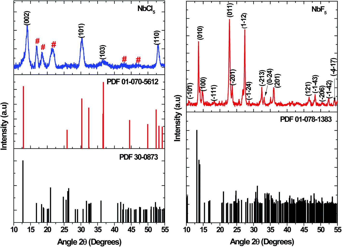
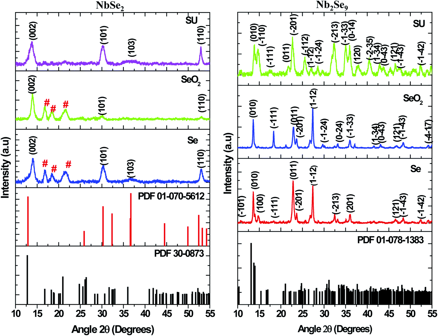
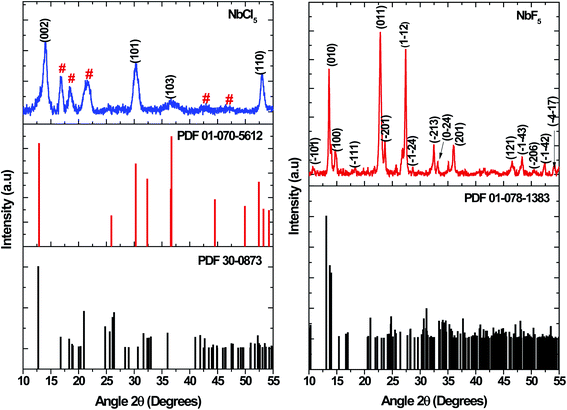
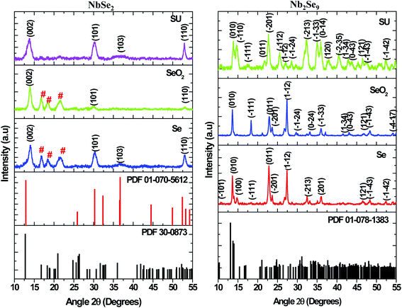
Metal precursors have been shown to influence the properties of nanostructures due to their reactivity. Metal chlorides, acetate, and nitrates have been commonly used as precursors for synthesis of both metal chalcogenides and oxides. Herein, the effect of using NbCl5 and NbF5 on the resultant nanostructures was investigated. Shown in Fig. 1 are the X-ray diffraction patterns of particles synthesized by varying the niobium precursor. The use of NbCl5 resulted in the formation of 2H–NbSe2 (PDF 01-070-5612) and also oxide impurities in the form of T–Nb2O5 denoted by # (PDF 30-0873). Changing the precursor to NbF5 resulted in the formation of Nb2Se9 (PDF 01-078-1383), with no impurities detected.
 |
| | Fig. 1 XRD patterns of particles synthesized from NbCl5 and NbF5 precursors. | |
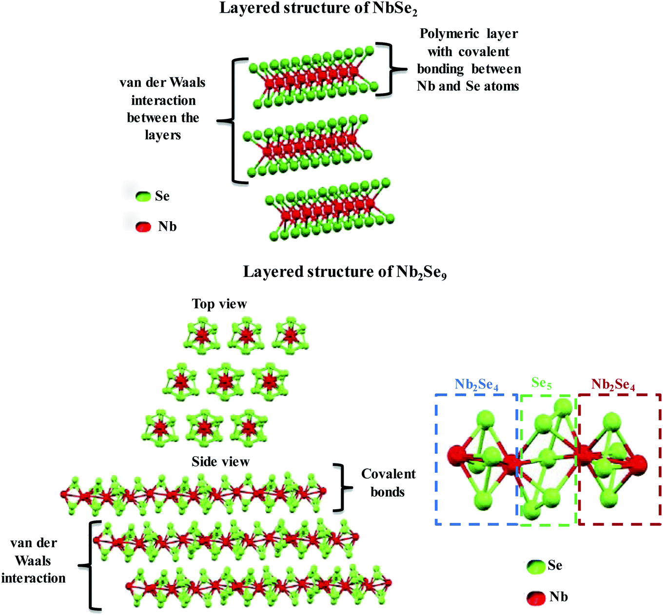
The two stoichiometries (NbSe2 and Nb2Se9), differ in structure as shown in Fig. 2. NbSe2 has a crystal structure containing polymeric layers with the Nb-layer sandwiched between two Se-layers (i.e. Se–Nb–Se). The Nb and Se atoms are covalently bonded whilst each polymeric layer is held together by weak van der Waals interactions. The layers are closely packed and the arrangement of up to 6 layered structures has been reported.23 The weak van der Waals forces are responsible for the easy sliding of the layers relative to one another, thus providing a favourable matrix for intercalation reactions and exfoliation.24 The coordination around the Nb atom can either be a distorted octahedral or trigonal prismatic.23 On the other hand, Nb2Se9 is a new 1D material made up of periodically stacked single-chain atomic crystals, which form the inorganic bulk of the crystals due to strong covalent bonds within the chain and weak van der Waals interaction between the chains, as shown in Fig. 2.25 It is similar to the structure of NbSe2 but it has chains and not polymeric sheets. Each Nb2Se9 chain is made up of Nb2Se4–Se5–Nb2Se4–Se5 sequence along the c-axis.24,25 Nb2Se4 forms a cage, each Nb atom is surrounded by one Se5 and two Se2 units thus coordinated to eight Se atoms.25 Therefore, Nb can be considered to have bicapped-trigonal prismatic coordination around it. The Nb atoms form non-linear chains because of the alternating long and short bonds with distances of 3.76 Å and 2.89 Å, respectively.25
 |
| | Fig. 2 Chemical structure of NbSe2 and Nb2Se9 layered materials. | |
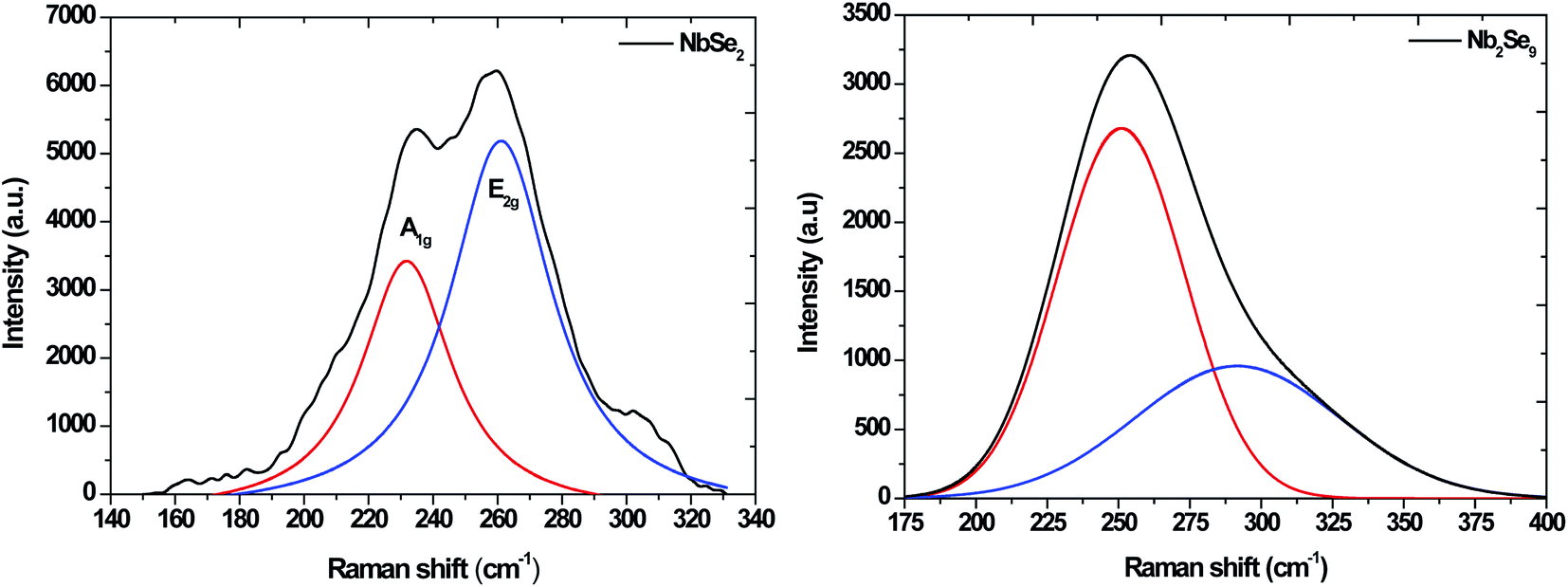
The Raman spectra for NbSe2 and Nb2Se9 are shown in Fig. 3. The NbSe2 spectrum has two characteristic peaks, the out of plane A1g peak and the in plane E2g peak at 225 and ∼245 cm−1, respectively.26 On the other hand, the vibrational modes of Nb2Se9 were at 239.62 cm−1 due to two Nb atoms vibrating along the (101) plane and the two Se pairs with a stretching motion.27 The second vibrational motion at 284.18 cm−1 was due to two pairs of stretching Nb atoms crossed and all the Se atoms vibrating in the outward direction at the same time.28
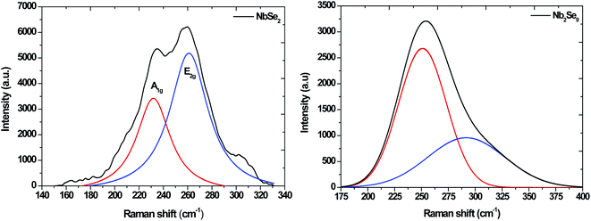 |
| | Fig. 3 Raman spectra of NbSe2 and Nb2Se9 materials synthesized from when varying the niobium precursors. | |
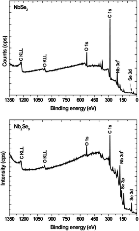
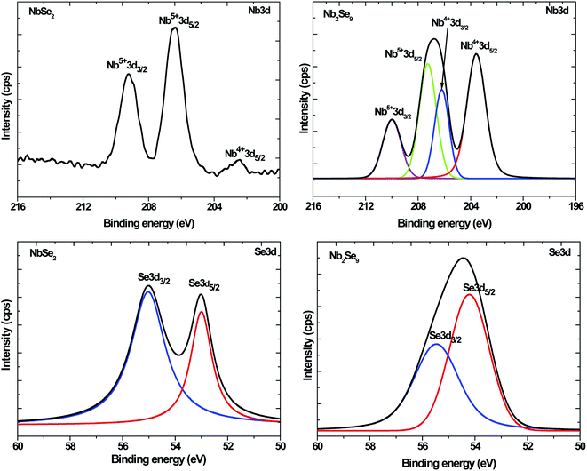
To further elucidate the structures, XPS was undertaken. Shown in Fig. 4 are the XPS survey spectra of the as-synthesized particles. Both spectra showed the presence of Nb, Se, C and O. The C is due to the capping agent and the O is because of the oxidation of the capping agent as well as the Nb2O5 in the NbCl5 derived particles as observed in XRD.
 |
| | Fig. 4 XPS survey spectra of NbSe2 and Nb2Se9 when varying the niobium precursors. | |
To fully understand the chemical species present, high-resolution spectra were recorded. The C1s and O1s for both NbSe2 and Nb2Se9 particles showed a presence of C–C, C–O, and C![[double bond, length as m-dash]](https://www.rsc.org/images/entities/char_e001.gif) O emanating from the capping agent (Fig. 1S†). The C–O and CO bonds are indicative of oxidation of the capping agent.29 As such the capping does provide a protective layer and hence minimizes the oxidation of the core inorganic particle. Nevertheless, some oxidation of the inorganic core was observed as evidenced by the detection of an M–O species in both NbSe2 and Nb2Se9 O1s core level spectra. The extent of the oxidation is however different. The NbSe2 was more oxidized than Nb2Se9 as shown in Table 3 and also observed as T–Nb2O5 in the XRD pattern.
O emanating from the capping agent (Fig. 1S†). The C–O and CO bonds are indicative of oxidation of the capping agent.29 As such the capping does provide a protective layer and hence minimizes the oxidation of the core inorganic particle. Nevertheless, some oxidation of the inorganic core was observed as evidenced by the detection of an M–O species in both NbSe2 and Nb2Se9 O1s core level spectra. The extent of the oxidation is however different. The NbSe2 was more oxidized than Nb2Se9 as shown in Table 3 and also observed as T–Nb2O5 in the XRD pattern.
Table 3 Summary of the atomic composition and stoichiometric assignments obtained from the fitting of the XPS spectra reported in ESI Fig. 1S and 5
| Precursor |
Element |
Atomic% |
Peak binding energy (eV) |
Assignments |
Assignment% |
| NbCl5 |
C |
85.3 |
284.8 |
C–C |
78.6 |
| 286.3 |
C–O |
4.7 |
| 288.8 |
O–CO |
1.9 |
| O |
10.2 |
530.2 |
M–O |
5.4 |
| 531.7 |
CO |
4.1 |
| 533.3 |
C–O |
2.4 |
| Nb |
2.9 |
203.0 |
Nb4+3d5/2 |
0.1 |
| 206.9 |
Nb5+3d5/2 |
1.5 |
| 209.3 |
Nb5+3d3/2 |
0.4 |
| Se |
1.5 |
53.4 |
Se3d5/2 |
0.7 |
| 55.5 |
Se3d3/2 |
0.6 |
| NbF5 |
C |
77.9 |
284.9 |
C–C |
59.5 |
| 286.2 |
C–O |
6.0 |
| 288.7 |
O–CO |
4.1 |
| O |
13.3 |
530.1 |
M–O |
2.8 |
| 531.8 |
CO |
5.5 |
| 533.6 |
C–O |
4.4 |
| Nb |
2.5 |
203.6 |
Nb4+3d5/2 |
1.6 |
| 206.3 |
Nb4+3d5/2 |
1.6 |
| 207.3 |
Nb5+3d3/2 |
1.3 |
| 210.1 |
Nb5+3d5/2 |
1.6 |
| Se |
6.3 |
54.2 |
Se3d5/2 |
8.3 |
| 55.4 |
Se3d3/2 |
3.7 |
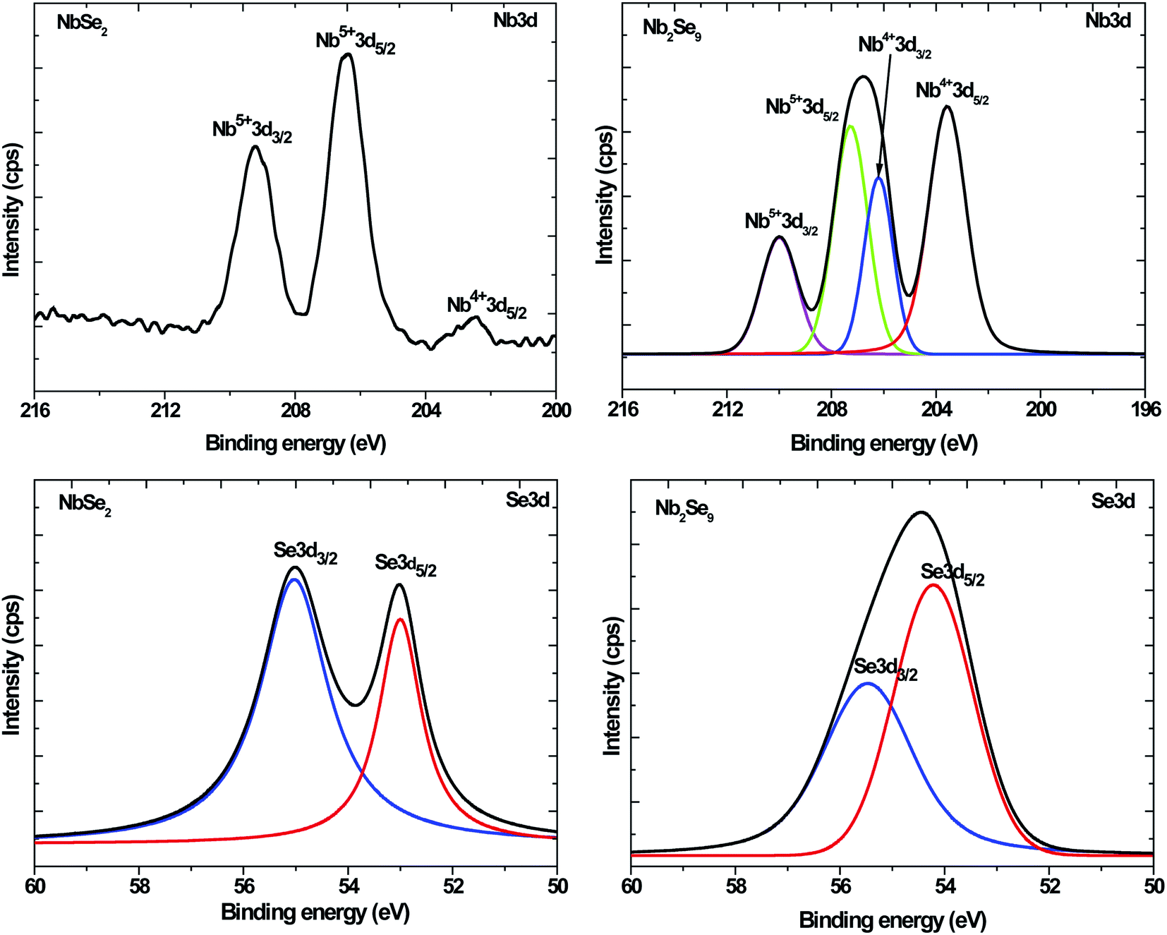
Fig. 5 shows the Nb3d and Se3d core-level spectra of NbCl5 and NbF5 derived NbSe2 and Nb2Se9 nanostructures respectively. The NbSe2 Nb3d core level spectrum showed three components, composed of the Nb4+3d5/2 (203.0 eV), the Nb5+3d5/2 (206.9 eV) and the Nb5+3d3/2 (209.3 eV). The Nb4+3d5/2 and the Nb4+3d3/2 peaks corresponded to NbSe2 while the Nb5+3d5/2 corresponded to Nb2O5. These results were consistent with work reported by Boscher et al.30 The NbSe2 Se3d core level spectrum showed two peaks all attributed to the NbSe2.
 |
| | Fig. 5 Nb3d and Se3d XPS core-level spectra for NbSe2 and Nb2Se9 when varying the niobium precursors. | |
For Nb2Se9, the Nb3d core level spectrum showed four peaks assigned to Nb4+3d5/2 (203.6 eV), Nb4+3d5/2 (206.3 eV), Nb5+3d5/2 (207.3 eV), and Nb5+3d5/2 (210.0 eV) corresponding to Nb2Se9 and Nb2O5 similar to the NbSe2 spectrum. The XRD pattern of NbF5 derived particles showed no evidence of Nb2O5. This suggests that the extent of metal oxidation is not as pronounced in Nb2Se9 since XRD is a bulk technique. The % composition of the present chemical species is summarized in Table 3. The % atomic composition of O was more in NbF5 derived particles compared to NbCl5 derived particles (13.3% and 10.2% respectively), however from the assignment%, NbF5 derived particles had the least amount attributed to M–O (2.8%) suggesting that most of the oxidation occurred in the organic capping layer.
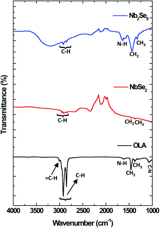
The nature of the capping of the nanostructures can be further investigated using FT-IR and spectroscopy. The FT-IR spectra of the as-synthesized OLA-capped NbSe2 and Nb2Se9 nanostructures are illustrated in Fig. 6. Three main functional groups were identified in pure OLA. These functional groups were C–N, CH2/CH3 and N–H. The C–N and N–H peaks located at 1071 cm−1 and 1593 cm−1 respectively, decreased in intensity in the NbSe2 spectrum compared to the pure OLA. On the other hand, in the FT-IR spectrum of Nb2Se9, the C–N peak disappeared and the N–H peak was shifted as well as broadened compared to the pure OLA. This confirms that there is a change in the terminal functional group (–NH2) in OLA. As such, this further confirms that OLA has capped the surface of these nanostructures.31
 |
| | Fig. 6 FT-IR spectra of oleylamine (OLA), NbSe2 and Nb2Se9 when varying the niobium precursors. | |
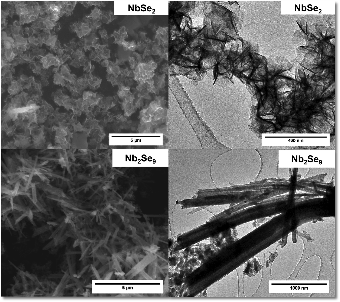
To study the morphological properties of the resultant materials, SEM and TEM studies were undertaken. Shown in Fig. 7 are the SEM and TEM images of the particles synthesized from the two metal precursors. The NbSe2 particles showed sheet-like morphology. This is consistent with 2D layered materials. From SEM, the sheets are arranged in a flower-like pattern. Colloidal synthesized nanosheets tend to have high surface energies hence they fold over each other forming architectures such as the nanoflowers to minimize the surface energy.32 Although the focus of many studies has been on flat nanosheets, assembly into 3D nanoflowers has advantages such as high specific surface area, broad internal space, mechanical stability, and easy accessibility to catalytically active sites.33 The presence of many edge sites is advantageous for electrocatalytic applications as edge sites are more catalytically active than the basal planes of the material.34 On the other hand, NbF5 derived particles showed rod-like morphology. The rod-like structures are consistent with the crystal structure of Nb2Se9 shown in Fig. 2. This is also in line with the work reported by Lee et al.4
 |
| | Fig. 7 SEM and TEM micrographs of NbSe2 and Nb2Se9 when varying the niobium precursors. | |
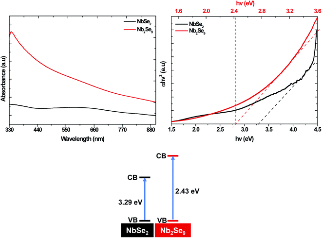
To study the optical properties of the resultant materials, UV-vis absorption spectroscopy was undertaken and the results are shown in Fig. 8. The band-gap of NbSe2 (3.29 eV) was firmly on the UV region while the band-gap of Nb2Se9 was in the visible region (2.43 eV). This suggests that by altering the precursor, one can alter the optical properties.
 |
| | Fig. 8 UV-vis absorption spectra and Tauc plot of NbSe2 and Nb2Se9 when varying the niobium precursors. | |
 |
| | Fig. 9 Molecular structure of NbCl5 and NbF5. | |
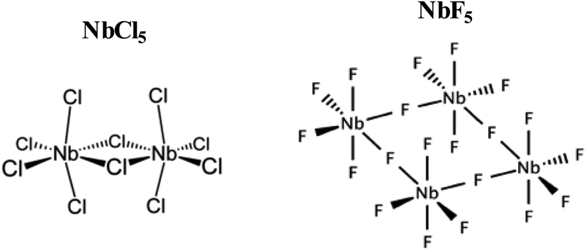
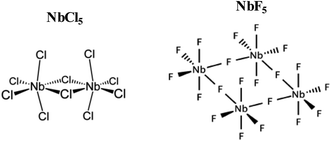
Based on the obtained results, the mechanism of formation of NbSe2 and Nb2Se9 was deduced. In the colloidal heat-up method, the decomposition of the precursors (Fig. 9) drives the formation of the nuclei. Based on the HSAB theory, Nb5+ is a hard Lewis acid, and F− is a harder Lewis base compared to Cl−, as such, Nb5+ forms a more stable complex with F− than Cl−.35 As a result, the decomposition chemistry of the two compounds will be different. Nb5+ has tightly held outer electrons and vacant orbitals available that are not too high in energy. These orbitals can accept electrons from the ligand such as F to form π bonds.35 Also, pentahalides have diversity in their structure. For example, NbCl5 has a dimer structure (i.e. two Cl bridges)36 whereas NbF5 has a tetramer structure (i.e. four F bridges) within a single unit cell (Fig. 7).37 In a typical dimer, there are (NbCl5)2 units, the bridge-bonds are longer and weak which causes the axial bonds to bend inward.38 A tetramer structure of NbF5 contains (NbF5)4 units, each unit are connected by an F-bridge forming a square.38 Hence, the nucleation and growth process of nanoparticles will be affected. The formation of NbSe2 and Nb2Se9 from NbCl5 and NbF5 respectively occur based on the following reactions:
| | |
2NbCl5 + 4Se → 2NbSe2 + 5Cl2
| (1) |
| | |
2NbF5 + 9Se → Nb2Se9 + 5F2
| (2) |
Using the TEM images of NbSe2 and Nb2Se9 at different time intervals as shown in Fig. 10, the mechanism for the formation of the different morphologies is postulated. NbSe2 nanoflowers begin with the formation of layered flocculates after 5 min which is essentially the starting material. Savjani et al. reported that MoS2 initially forms flocculates, which are known to have lateral dimensions ranging from hundreds to thousands of nanometers.39 Guo et al. reported that the formation of nanosheets is due to low supersaturation which allows growth to occur in two directions.15 These lateral flocculates, slide over one another due to the weak van der Waals forces and begin to curl as shown in the 30 min sample. Finally, after 120 min nanoflowers are formed by completely curled nanosheets. Nb2Se9 nanostructures form quicker than NbSe2 nanostructures as rods were already observed at 5 min. The formation of the rods is also postulated to form from layered flocculates and these flocculates also slide over each other similar to NbSe2, however, the sliding is not as pronounced. This is shown by the unevenness of the edges of the rods in the 5 min TEM image. After 120 min, the flocculates slide next to each forming chains that result in elongated rods. This is synonymous with the chain-like crystal structure expected for Nb2Se9. The small dot-like particles on the image are thought to be Nb2O5 nanoparticles.
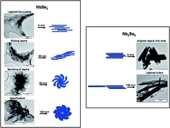 |
| | Fig. 10 Formation mechanism of NbSe2 and Nb2Se9 when varying the niobium precursors. | |
Varying the selenium precursor
Seeing that changing the metal precursor resulted in the formation of different niobium selenide crystal phases hence properties, the selenium precursors were also varied. Three precursors were used, namely elemental selenium (Se), selenium dioxide (SeO2), and selenourea (SU). Selenium is a non-metal that has similar properties to sulfur and tellurium. SeO2 is a one-dimensional polymer that consists of alternating selenium and oxygen atoms. Each Se atom is pyramidal and bears a terminal oxide group. The stereochemistry at Se alternates along the polymer chain hence resulting in a syndiotactic polymer.40 Selenourea is an organoselenium compound. This compound features an unhindered carbon–selenium double bond.
Shown in Fig. 11 are the X-ray diffractograms of NbSe2 nanostructures emanating from NbCl5 and different selenium precursors. The particles synthesized using Se as previously shown in Fig. 1 and SeO2 were indexed to a hexagonal 2H–NbSe2 phase (PDF 01-070-5612) indicated by the black hkl indices. Also, there were three high-intensity peaks (#) between 2θ values 15–25° indexed to an orthorhombic phase of T–Nb2O5 (PDF 30-0873). On the other hand, the particles synthesized from SU precursor were pure and consistent with a rhombohedral phase 3R–NbSe2 (PDF 01-070-1620). The peak positions of the 2H–NbSe2 and 3R–NbSe2 are similar; however, there is a small shift towards lower angles for the rhombohedral phase as shown in Fig. 11. Also, the two phases have different lattice parameters, with a = 3.45 and c = 12.55 for the 2H-phase while a = 3.45 and c = 18.88 for the 3R-phase. The results from Nb2Se9 nanostructures emanating from NbF5 and different selenium precursors are also shown in Fig. 11. The particles from the various selenium precursors were all indexed to a Nb2Se9 triclinic phase (PDF 01-078-1383). However, the intensities of the peaks were different as such the crystallinity. The peaks from Se and SeO2 derived samples were more intense than the SU sample hence suggesting good crystallinity. The peak widths were much narrower for Se and SeO2 than SU nanoparticles; therefore, indicative of different sizes. From the XRD results, it is quite clear that the metal precursors are responsible for the stoichiometry of niobium selenide, NbCl5 result in NbSe2 whilst NbF5 results in Nb2Se9. In terms of the selenium precursors, Se and SeO2 due to their one-step reaction, they result in similar properties whilst SU involves a two-step synthetic route (first the decomposition of SU as in eqn (5) and the reaction with the metal precursors eqn (6) and (7)), as such, subtle differences in properties are observed. The reactions towards the formation of NbSe2 and Nb2Se9 using the different selenium precursors are shown in eqn (1)–(7).
| | |
2NbCl5 + 4SeO2 → 2NbSe2 + 4O2 + 5Cl2
| (3) |
| | |
2NbF5 + 9SeO2 → Nb2Se9 + 9O2 + 5F2
| (4) |
| | |
2CH4N2Se → 2H2Se + 2C(NH)2
| (5) |
| | |
2NbCl5 + 4H2Se → 2NbSe2 + 5Cl2 + 9H2
| (6) |
| | |
2NbF5 + 9H2Se → 2Nb2Se9 + 5F2 + 9H2
| (7) |
 |
| | Fig. 11 XRD patterns of NbSe2 and Nb2Se9 when varying the selenium precursors. | |
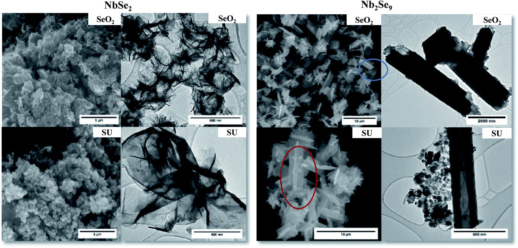
The SEM and TEM images using the SeO2 and SU as selenium precursors are shown in Fig. 12. For NbSe2, varying the selenium precursor did not change the morphology; the particles remained flower-like nanosheets however the SU samples had larger nanoflowers. For Nb2Se9, there was a slight change of morphology from the Se precursor in Fig. 7 to the SeO2 and SU precursors where perpendicular connected flat rods were formed as shown in the SEM images in Fig. 12. From the TEM, these were however very similar to the Se rods. HRTEM was also performed on the pure NbSe2 and Nb2Se9 (shown in Fig. 2S†) which formed using SU. The average interlayer spacing for NbSe2 layers is 0.61 nm, which is in agreement with the theoretical d-spacing for (002) planes.41,42 The same spacing was obtained for Nb2Se9 nanorods.
 |
| | Fig. 12 SEM and TEM images of NbSe2 and Nb2Se9 when varying the selenium precursors. | |
The UV-vis absorption spectra of NbSe2 and Nb2Se9 when varying the selenium precursors are shown in Fig. 3S† and the band-gap values are summarized in Table 4. For NbSe2 nanoflowers, the band-gap decreases from Se to SeO2 to SU. This is consistent with the observed increase in the size of the nanoflowers. An increase in size of the nanostructures results in the red-shift of the band-gap due to Ostwald ripening. The band-gap for Nb2Se9 remained relatively unchanged as the selenium precursor changed from Se to SeO2. This is expected as there were little changes observed in the structural and morphological properties between the two precursors. The band-gap for SU was however red-shifted. It must be said that from the absorption spectra in Fig. 3S,† the graphs were tailing suggesting polydispersity.
Table 4 Summary of the band-gaps of NbSe2 and Nb2Se9 when varying the selenium precursors
| Selenium precursor |
NbSe2 Eg |
Nb2Se9 Eg |
| Se |
3.29 eV |
2.43 eV |
| SeO2 |
2.91 eV |
2.44 eV |
| SU |
2.55 eV |
2.12 eV |
Application of NbSe2 and Nb2Se9 as counter electrodes in DSSCs
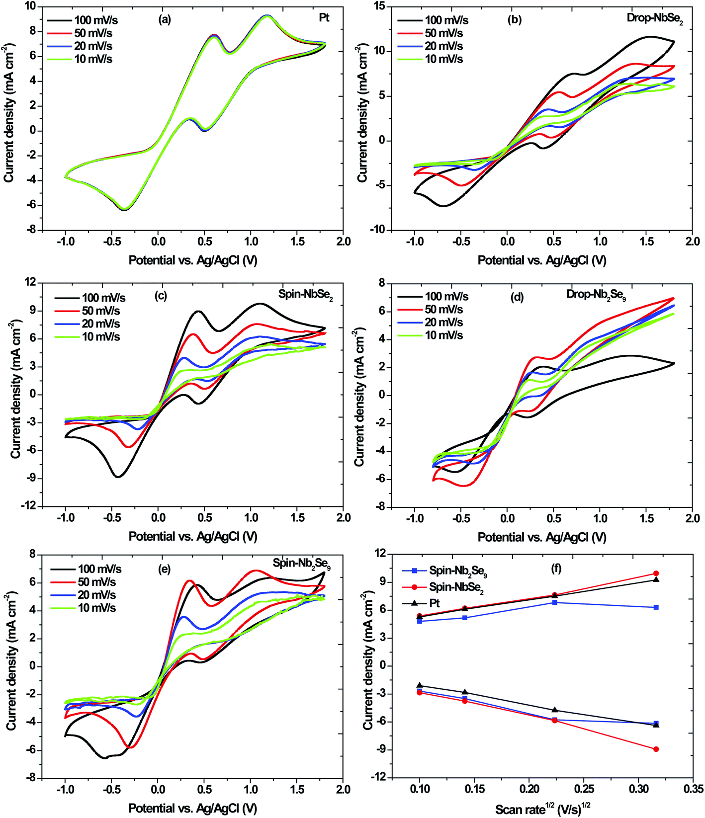
NbSe2 and Nb2Se9 nanostructures synthesized using SU as the selenium precursor were used as the counter electrodes. The electrocatalytic activity of the CEs was determined by cyclic voltammetry (CV), where the scan rate was varied to investigate the effect of the scan rate on the current density of each CE. Based on eqn (8), there exist a relationship between the current density and square root of the scan rate. As such, an increase in scan rate causes the diffusion layer thickness to decrease and the electrochemical polarization to increase which results in high overpotential and poor reversibility.43| | |
ip = 2.69 × 10⁵n3/2AD1/2V1/2C
| (8) |
where ip is the peak current density, n is the number of electrons transferred, A is the area of the electrode, D is the diffusion coefficient, V is the scan rate, and C is the concentration.43 The scan rates were 10, 20, 50 and 100 mV s−1 and the results are shown in Fig. 13. Typically, there are two pairs of redox peaks where the left pair is due to the reduction of I3− and the right pair is due to the oxidation of I− and they correspond to the following equations:
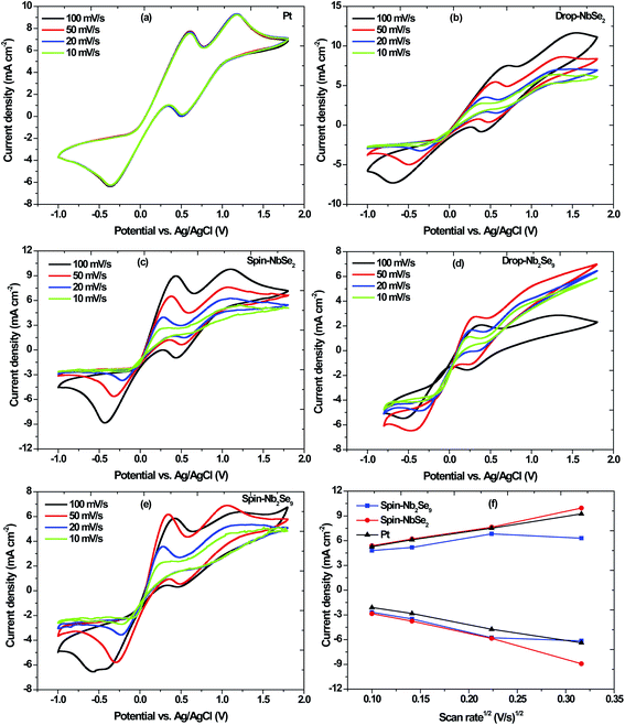 |
| | Fig. 13 Cyclic voltammograms at different scan rates of (a) sputtered Pt, (b) drop casted NbSe2, (c) spin coated NbSe2, (d) drop casted Nb2Se9 and (e) spin coated Nb2Se9; and (f) linear fitting of the capacitive current densities of Pt compared with the NbSe2 and Nb2Se9 CEs. | |
The Pt-CE, shown in Fig. 13a, is stable and reproducible irrespective of the scan rate used because the scans remained unchanged for each scan rate. The cathodic peaks appear at 0.36 V and 0.50 V. The performance of the DSSC depends on the reduction whereas as the oxidation does not have that much effect.44 Ibrahem et al. reported that in general, the higher the cathodic current peak the better the catalytic capability of the CE towards the reduction of I3− to I− in DSSCs.21
Two methods were used to fabricate the niobium selenide CEs i.e. drop casting and spin coating. The cyclic voltammograms of NbSe2 nanoflowers at different scan rates (10 mV s−1, 20 mV s−1, 50 mV s−1, and 100 mV s−1) are shown in Fig. 13b and c. The current densities increase with an increase in scan rate. The drop-casted CE has a lower current density compared to the spin-coated CE, with the value of 0.0087 A cm−2 and 0.0090 A cm−2 at a scan rate of 100 mV s−1. Moreover, the drop-casted CE's cathodic peaks are not as defined as those of the spin-coated CE. Therefore, the spin-coated CE has the better catalytic capability for the reduction of I3− to I−. The Nb2Se9 CEs were also analyzed, and the spin-coated CE seems to have a better capability of reducing I3− to I− than the drop-casted CE shown in Fig. 13d and e. Therefore, the Nb2Se9 spin-coated CE produces the desired results at 50 mV s−1 because it has the highest current density.
As proof of principle and to highlight the possibility of using niobium selenide CEs as alternatives to the Pt-CE, the two CEs (spin-coated: NbSe2 and Nb2Se9) were compared with the Pt-CE. The peak-to-peak separation (Epp) is an important parameter to look at when comparing the catalytic activity of electrodes.45 The cathodic peak represents the reduction velocity and the Epp is associated with the reversibility of the redox reaction.45 The Pt-CE has an Epp of 805 mV whereas NbSe2 and Nb2Se9 CEs are 819 and 762 mV, respectively. Therefore, the Nb2Se9-CE has better reversibility and electrocatalytic activity because it has a smaller Epp than the Pt-CE. However, the NbSe2-CE has a similar Epp as the Pt-CE. Moreover, the NbSe2-CE exhibited the highest current density compared to Nb2Se9-CE, which is an indication of better electrocatalytic activity. As such, of the two niobium selenide materials NbSe2 is a better CE than Nb2Se9 because of its comparable Epp and higher current density than that of Pt. This is because the NbSe2 nanoflowers that are essentially nanosheets that are ‘crumbled up’ have the largest surface area and better coverage of the FTO-glass substrate than the Nb2Se9 nanorods.45 To verify the surface area, the relationship between the current density and square root of the scan rate was plotted in Fig. 13f based on eqn (8). The electrochemical double-layer capacitance (Cdl) of NbSe2-CE was much larger than Nb2Se9-CE (slope), therefore suggesting a greater effective surface area (S) (Cdl ∝ S).
The EIS was employed to evaluate the ability of the CEs to transfer charge to the electrolyte. Shown in Fig. 14 are the Nyquist plots of Pt, NbSe2 and Nb2Se9 as well as the electrochemical equivalent circuit whose components represent four impedance properties. The series resistance is denoted by, Rs while Rct denotes the charge transfer resistance at the CE/electrolyte interface. The abbreviation Cdl corresponds to the double layer capacitance, which is employed when a perfect semi-circle is obtained from the Nyquist plot and explains the charge storage capacity of the CEs. Lastly, Zw represents the Nernst diffusion element, often employed when a line is at 45° to the semi-circle at lower frequency region and explains if the interaction between the CE and the electrolyte is diffusion-controlled.46 The two key parameters, Rs and Rct were obtained using Z-fit in EC-Chem software from Biologic and are summarized in Table 5. The Pt had the lowest Rs value followed by NbSe2 and then Nb2Se9. The smaller the Rs value, the more conductive the material is. This suggests that Pt is the most conductive. The same trend was observed for Rct however, the charge transfer resistance for Pt was far much lower than NbSe2. Lower Rct values are sort-after because they lead to higher Jsc and FF values. It must be added that thin-film quality has a significant influence on the electrical properties of materials. The sputtered Pt electrode had far better coverage than NbSe2 and Nb2Se9.
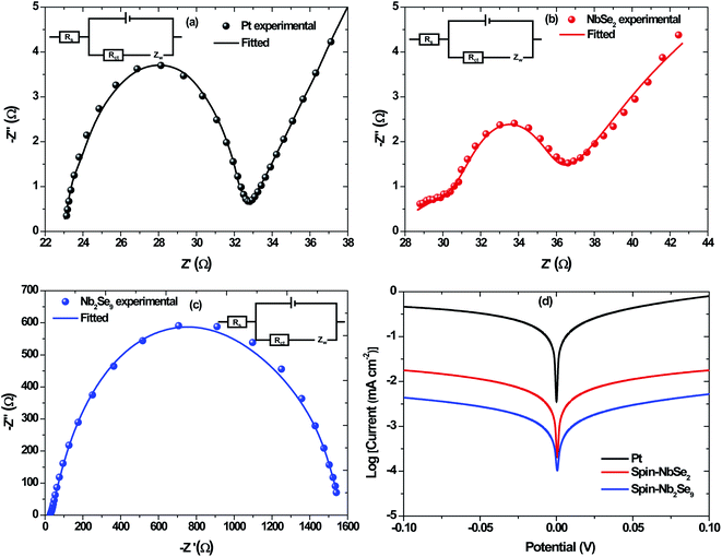 |
| | Fig. 14 Nyquist plots of EIS for the symmetric cells with (a) Pt, (b) spin-NbSe2 and (c) spin-Nb2Se9 and the corresponding Tafel plots (d). | |
Table 5 Electrochemical performance parameters obtained from EIS & Tafel polarization plots of Pt, spin-NbSe2 and spin-Nb2Se9
| Materials |
Rs/Ω |
Rct/Ω |
logJ0/(mA cm−2) |
logJlim/(mA cm−2) |
| Pt |
23.04 |
9.41 |
−5.47 |
−5.38 |
| Spin-NbSe2 |
27.38 |
36.14 |
−6.01 |
−9.92 |
| Spin-Nb2Se9 |
27.58 |
1033 |
−6.85 |
−12.1 |
The Tafel polarization curves are shown in Fig. 14d. Two important parameters are observed from the polarization curves, namely the exchange current density (J0) and the limiting diffusion current density (Jlim). Both parameters are affected by the anodic or cathodic contribution of each counter electrode and can be described using the following equation;
where
R is the gas constant,
T is the temperature (298 K),
F is Faraday's constant,
n (
n = 2) is the number of electrons,
Rct is the charge transfer resistance,
D the diffusion coefficient,
C is the concentration of I
3−, and
l is the spacer thickness.
47 From
eqn (11),
J0 is inversely proportional to
Rct. Therefore,
J0 can be correlated to the electrocatalytic activity of the CE, meaning a large
J0 value implies a much better catalytic activity. Similarly, larger
Jlim values indicate the larger diffusion coefficient
D, which results in higher catalytic activity based on
eqn (12). The
J0 value of NbSe
2 was higher than Nb
2Se
9 symbolizing the best electrocatalytic activity. So too was the
Jlim value. In both the EIS analysis and Tafel polarization curves, Pt was the best performing electrode. This was not surprising as Pt is considered the state-of-the-art counter electrode, furthermore visually; the Pt thin film was uniform.
The Pt, NbSe2 and Nb2Se9 CEs were used in DSSCs. Shown in Fig. 15 is the solar cell architecture, band structure and the resultant current density–voltage (J–V) curves of the three CEs and the results are also summarized in Table 6. The NbSe2 solar cell had the highest PCE of 6.84% compared to the other electrodes. This was in the same order as the reported results for NbSe2 DSSCs.21 The Pt base DSSC surprising had a lower efficiency, contrary to the electrochemical results. This could be because of the fabrication process. The Nb2Se9 had the lowest efficiency, which is consistent with the electrochemical data. The superior performance of NbSe2 over Nb2Se9 can be attributed to the morphology of the nanostructures. The NbSe2 nanoflowers has a larger apparent surface area compared to Nb2Se9 nanorods. Also notably from Fig. 15 and the data in Table 6 are the low FF values. The low FF values are due to the high Rs values and low shunt resistance (Rsh) values, which are caused by increasing recombination at interfaces of the DSSCs.48
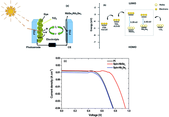 |
| | Fig. 15 (a) Dye-sensitized solar cell set-up, (b) band diagram and (c) J–V curves of DSSCs of Pt, spin-NbSe2 and spin-Nb2Se9 counter electrodes. | |
Table 6 J–V parameters of DSSCs of Pt, spin-NbSe2 and spin-Nb2Se9 counter electrodes
| Counter electrode |
Jsc (mA cm−2) |
Voc (V) |
FF (%) |
PCE (%) |
| Pt |
12.00 |
0.77 |
34 |
3.14 |
| Spin-NbSe2 |
13.00 |
0.95 |
55 |
6.84 |
| Spin-Nb2Se9 |
10.00 |
0.76 |
37 |
2.80 |
4. Conclusion
In summary, niobium selenide nanostructures were formed using the colloidal method. Varying the metal precursors resulted in the formation of different stoichiometries of niobium selenide. The NbCl5 and NbF5 resulted in the formation of NbSe2 and Nb2Se9, respectively. While maintaining the two different metal precursors and varying the selenium precursor from Se, SeO2 to SU, the properties of NbSe2 and Nb2Se9 changed slightly however the effect of changing the selenium precursor was less pronounced than changing the metal precursors. From the XRD and XPS, the NbSe2 nanostructures were more susceptible to oxidation than Nb2Se9 as Nb2O5 was observed in the XRD and the percentage of M–O in the XPS was much higher in NbSe2. The nanostructures were capped by OLA as observed in the FT-IR spectroscopy thus minimizing the oxidation. NbSe2 generally formed nanoflowers whilst Nb2Se9 formed rods. The band-gaps of both NbSe2 and Nb2Se9 were in the visible region and there were red-shifted as the selenium precursor was altered. The spin coated NbSe2 and Nb2Se9 were used successfully as electrocatalysts in DSSCs. NbSe2 nanoflowers gave the best performance with 6.84% PCE.
Conflicts of interest
There are no conflicts to declare.
Acknowledgements
The authors would like to thank the University of the Witwatersrand, School of Chemistry; the Wits Microscope and Microanalysis Unit and the National Research Foundation (NRF) for funding of this work.
References
- S. Memaran, N. R. Pradhan, Z. Lu, D. Rhodes, J. Ludwig, Q. Zhou, O. Ogunsolu, P. M. Ajayan, D. Smirnov and D. Fernández-Domínguez, Nano Lett., 2015, 15, 7532–7538 CrossRef CAS PubMed.
- S. M. M. Nelwamondo, M. J. Moloto, R. W. Krause and N. Moloto, Mater. Res. Bull., 2012, 47, 4392–4397 CrossRef CAS.
- L. F. E. Machogo, P. Tetyana, R. Sithole, S. S. Gqoba, N. Phao, M. Airo, P. M. Shumbula, M. J. Moloto and N. Moloto, Appl. Surf. Sci., 2018, 456, 973–979 CrossRef CAS.
- C. Lee, X. Wei, J. W. Kysar and J. Hone, Science, 2008, 321, 385–388 CrossRef CAS PubMed.
- S. Chae, A. J. Siddiqa, S. Oh, B. J. Kim, K. H. Choi, W. Jang, Y. Kim, H. K. Yu and J. Choi, Nanomaterials, 2018, 8(10), 794 CrossRef PubMed.
- P. Joensen, R. F. Frindt and S. R. Morrison, Mater. Res. Bull., 1986, 21, 457–461 CrossRef CAS.
- M. A. Ibrahem, W.-C. Huang, R.-W. Lan, K. M. Boopathi, Y. C. Hsiao, C. H. Chen, C.-S. Chang, L.-J. Li, C.-H. Tsai and C. W. Chu, J. Mater. Chem. A, 2014, 2, 11382–11390 RSC.
- R. Qu, X. Wen, Y. Zhao, T. Wang, R. Yao and J. Lu, Ultrason. Sonochem., 2021, 73, 105491 CrossRef CAS PubMed.
- J. Liu, X. Sui, S. Zhang, S. Xu and J. Hao, Tribology, 2018, 38, 635–644 Search PubMed.
- T. Tsuneta, T. Toshima, K. Inagaki, T. Shibayama, S. Tanda, S. Uji, M. Ahlskog, P. Hakonen and M. Paalanen, Curr. Appl. Phys., 2003, 6, 473–476 CrossRef.
- F. O.-T. Agyapong-Fordjour, S. Oh, J. Lee, S. Chae, K. H. Choi, S. H. Choi, S. Boandoh, W. Yang, J. Huh, K. K. Kim and J.-Y. Choi, ACS Appl. Energy Mater., 2019, 2, 5785–5792 CrossRef CAS.
- B. J. Kim, B. J. Jeong, S. Oh, S. Chae, K. H. Choi, T. Nasir, S. H. Lee, K.-W. Kim, H. K. Lim, I. J. Choi, L. Chi, S.-H. Hyun, H. K. Yu, J.-H. Lee and J.-Y. Choi, RSC Adv., 2018, 8, 37724–37728 RSC.
- F. Kadijk and F. Jellinek, J. Less-Common Met., 1971, 23, 437–441 CrossRef CAS.
- P. Sekar, E. C. Greyson, J. E. Barton and T. W. Odom, J. Am. Chem. Soc., 2005, 127, 2054–2055 CrossRef CAS PubMed.
- J. Guo, Y. Shi, C. Zhu, L. Wang, N. Wang and T. Ma, J. Mater. Chem. A, 2013, 1, 11874–11879 RSC.
- V. K. Lamer and R. H. Dinegar, J. Am. Chem. Soc., 1950, 72(11), 4847–4854 CrossRef CAS.
- J. Van Embden, A. S. R. Chesman and J. J. Jasieniak, Chem. Mater., 2015, 27, 2246–2285 CrossRef CAS.
- M. Wu, Y. Wang, X. Lin, N. Yu, L. Wang, L. Wang, A. Hagfeldt and T. Ma, Phys. Chem. Chem. Phys., 2011, 13, 19298–19301 RSC.
- E. Singh, K. S. Kim, G. Y. Yeom and H. S. Nalwa, RSC Adv., 2017, 7, 28234 RSC.
- J. Liang, J. Li, H. Zhu, Y. Han, Y. Wang, C. Wang, Z. Jin, G. Zhang and J. Liu, Nanoscale, 2016, 8, 16017–16025 RSC.
- M. A. Ibrahem, W. Huang, T. Lan, K. M. Boopathi, Y. Hsiao, C. Chen, W. Budiawan, Y. Chen, C. Chang, L. Li, C. Tsai and C. W. Chu, J. Mater. Chem. A, 2014, 2, 11382 RSC.
- J. Guo, Y. Shi, C. Zhu, L. Wang, N. Wang and T. Ma, J. Mater. Chem. A, 2013, 1, 11874–11879 RSC.
- S. B. Artemkina, T. Y. Podlipskaya, A. I. Bulavchenko, A. I. Komonov, Y. V. Mironov and V. E. Fedorov, Colloids Surf., A, 2014, 461, 30–39 CrossRef CAS.
- W. Lee, S. Chae, Y. K. Chung, S. Oh, J. Choi and J. Huh, Phys. Status Solidi RRL, 2018, 1800517 Search PubMed.
- R. Sanjines, H. Berger and F. Levy, Mater. Res. Bull., 1988, 23, 549–553 CrossRef CAS.
- S. Naik, G. K. Pradhan, S. G. Bhat, B. C. Behera, P. S. A. Kumar, S. L. Samal and D. Samal, Phys. C, 2019, 561, 18–23 CrossRef CAS.
- J. Lee, B. J. Kim, Y. K. Chung, W. Lee, I. J. Choi, S. Chae, S. Oh, J. M. Kim, J. Choi and J. Huh, J. Raman Spectrosc., 2020, 51, 1100–1107 CrossRef CAS.
- M. Devaraj, R. Saravanan, R. Deivasigamani, V. K. Gupta, F. Gracia and S. Jayadevan, J. Mol. Liq., 2016, 221, 930–941 CrossRef CAS.
- R. K Sithole, L. F. E. Machogo, M. A. Airo, S. S. Gqoba, M. J. Moloto, P. Shumbula, J. Van Wyk and N. Moloto, New J. Chem., 2018, 42, 3042–3049 RSC.
- N. D. Boscher, C. J. Carmalt and I. P. Parkin, Eur. J. Inorg. Chem., 2006, 1255–1259 CrossRef CAS.
- S. Cao, T. Liu, W. Zeng, S. Hussain, X. Peng and F. Pan, J. Mater. Sci.: Mater. Electron., 2014, 25, 4300–4305 CrossRef CAS.
- A. Prabakaran, F. Dillon, J. Melbourne, L. Jones, R. J. Nicholls, P. Holdway, J. Britton, A. A. Koos, A. Crossley, P. D. Nellist and N. Grobert, Chem. Commun., 2014, 50, 12360–12362 RSC.
- S. H. Ahn and A. Manthiram, Adv. Energy Mater., 2016, 6, 1–7 Search PubMed.
- R. G. Pearson, J. Chem. Educ., 1968, 45, 643–648 CrossRef CAS.
- J. Chatt, Nature, 1956, 177, 852 CrossRef CAS.
- F. A. Cotton and G. Wilkinson, Advanced Inorganic Chemistry, John Wiley & Sons, New York, 5th edn, 1988 Search PubMed.
- W. Hönle, S. Furuseth and H. G. Schnering, Z. Naturforsch., B: J. Chem. Sci., 1990, 45, 952–956 CrossRef.
- A. F. Holleman, E. Wiberg and N. Wiberg, Inorganic Chemistry, 2001 Search PubMed.
- N. Savjani, E. A. Lewis, M. A. Bissett, J. R. Brent, R. A. Dryfe, S. J. Haigh and P. O'Brien, Chem. Mater., 2016, 28(2), 657–664 CrossRef CAS.
- F. A. Devillanova, Handbook of Chalcogen Chemistry: New Perspectives in Sulfur, Selenium and Tellurium, Royal Society of Chemistry, 2007, ISBN 9780854043668 Search PubMed.
- B. Xu, X. Ma, J. Tian, F. Zhao, Y. Liu, B. Wang, H. Yang and Y. Xia, Ionics, 2019, 25, 4171–4177 CrossRef CAS.
- Q. Shi, H. Zhu and L. Dang, J. Phys.: Conf. Ser., 2020, 1549, 032085 CrossRef CAS.
- M. Wu, Y. Wang, X. Lin, N. Yu, L. Wang, L. Wang, A. Hagfeldt and T. Ma, Phys. Chem. Chem. Phys., 2011, 13, 19298–19301 RSC.
- Z. Huang, X. Liu, K. Li, D. Li, Y. Luo, H. Li, W. Song, L. Chen and Q. Meng, Electrochem. Commun., 2007, 9, 596 CrossRef CAS.
- J. Roy-Mayhew, D. Bozym, C. Punckt and I. Aksay, ACS Nano, 2010, 4, 6203 CrossRef CAS PubMed.
- G. Yue, W. Wu, X. Liu and H. Zheng, Sol. Energy, 2018, 167, 137–146 CrossRef CAS.
- X. Qian, H. Li, L. Shao, X. Jiang and L. Hou, ACS Appl. Mater. Interfaces, 2016, 8, 29486–29495 CrossRef CAS PubMed.
- Z. Huang, G. Natu, Z. Ji, M. He, M. Yu and Y. Wu, J. Phys. Chem. C, 2012, 116, 26239–26246 CrossRef CAS.
Footnote |
| † Electronic supplementary information (ESI) available. See DOI: 10.1039/d0ra10894d |
|
| This journal is © The Royal Society of Chemistry 2021 |
Click here to see how this site uses Cookies. View our privacy policy here. 
 Open Access Article
 This Open Access Article is licensed under a Creative Commons Attribution-Non Commercial 3.0 Unported Licence
 *a
*a