
 Open Access Article
 This Open Access Article is licensed under a
 Creative Commons Attribution 3.0 Unported Licence
Challenges and prospects about the graphene role in the design of photoelectrodes for sunlight-driven water splitting
Saulo A. Carminati†
 a,
Ingrid Rodríguez-Gutiérrez†bc,
Andreia de Moraisd,
Bruno L. da Silvaa,
Mauricio A. Meloe,
Flavio L. Souza*abc and
Ana F. Nogueira*a
a,
Ingrid Rodríguez-Gutiérrez†bc,
Andreia de Moraisd,
Bruno L. da Silvaa,
Mauricio A. Meloe,
Flavio L. Souza*abc and
Ana F. Nogueira*a
aInstitute of Chemistry, University of Campinas (UNICAMP), PO Box 6154, Campinas, São Paulo 13083-970, Brazil. E-mail: flavio.souza@lnnano.cnpem.br; anafla@unicamp.br
bCentro de Ciências Naturais e Humanas, Universidade Federal do ABC (UFABC), Santo André, São Paulo 09210-580, Brazil
cBrazilian Nanotechnology National Laboratory (LNNano), Campinas, São Paulo 13083-970, Brazil
dCenter for Information Technology Renato Archer (CTI Renato Archer), Rodovia D. Pedro I, km 143.6, 13069-901, Campinas, SP, Brazil
eInstitute of Chemistry, Fluminense Federal University, Outeiro de São João Batista, Campus do Valonguinho, Niterói, Rio de Janeiro 24020-141, Brazil
First published on 16th April 2021
Abstract
Graphene and its derivatives have emerged as potential materials for several technological applications including sunlight-driven water splitting reactions. This review critically addresses the latest achievements concerning the use of graphene as a player in the design of hybrid-photoelectrodes for photoelectrochemical cells. Insights about the charge carrier dynamics of graphene-based photocatalysts which include metal oxides and non-metal oxide semiconductors are also discussed. The concepts underpinning the continued progress in the field of graphene/photoelectrodes, including different graphene structures, architecture as well as the possible mechanisms for hydrogen and oxygen reactions are also presented. Despite several reports having demonstrated the potential of graphene-based photocatalysts, the achieved performance remains far from the targeted benchmark efficiency for commercial application. This review also highlights the challenges and opportunities related to graphene application in photoelectrochemical cells for future directions in the field.
1 Introduction
Our society is facing a drastic environmental crisis associated with a significant dependence on non-renewable energy sources which release an uncontrollable amount of CO2 in the atmosphere. The scientific and industrial community efforts over the last decades have been spurred to develop carbon-free technologies. In this sense, artificial photosynthesis rises as one of the most elegant, sustainable, and renewable approaches to produce high energy density carriers, as molecules, driven by solar energy.Several semiconducting materials such as metal oxides, nitrides or sulphides have been synthesized and their performance continuously evaluated as photoelectrodes. Materials such as TiO2, ZnO, α-Fe2O3, WO3, BiVO4, WO3, Cu2O, CdS, CZTS and MoS2 are the most studied materials associated with their potential for photoelectrochemical (PEC) applications. However, significative drawbacks present in those materials such as in TiO2,1 WO3![[thin space (1/6-em)]](https://www.rsc.org/images/entities/char_2009.gif) 2 and ZnO3 related to their large band gap enabling them to absorb only small portion of the solar spectrum have prevented the technology development. Another common limitation reported is the surface recombination that reduces the material performance and can be exemplified by BiVO44 and α-Fe2O3.5 Cu-based materials have shown great performance in comparison with other cited system, however, it suffers with serious problem of chemical stability due to the photocorrosion process, shortening its lifetime as PEC component. To boost the PEC cell performance using photocatalysts, several strategies have been pursued, for instance, extending the absorption spectra towards infrared, improve charge carrier kinetics and increase the active sites at the surface including the doping with anions or cations,6–8 surface coupling with metals or semiconductors9,10 and film morphology design (nanoscaling).
2 and ZnO3 related to their large band gap enabling them to absorb only small portion of the solar spectrum have prevented the technology development. Another common limitation reported is the surface recombination that reduces the material performance and can be exemplified by BiVO44 and α-Fe2O3.5 Cu-based materials have shown great performance in comparison with other cited system, however, it suffers with serious problem of chemical stability due to the photocorrosion process, shortening its lifetime as PEC component. To boost the PEC cell performance using photocatalysts, several strategies have been pursued, for instance, extending the absorption spectra towards infrared, improve charge carrier kinetics and increase the active sites at the surface including the doping with anions or cations,6–8 surface coupling with metals or semiconductors9,10 and film morphology design (nanoscaling).
In this sense, carbon-based materials in nanometric scale have called the attention of many researchers in the field due to their properties and potential to improve optical and electronic of those mentioned semiconductors. It has been proved that the coupling between a semiconductor with carbon-based material can efficiently enhance the PEC activity by suppressing recombination, extending the excitation wavelength, or increasing the surface-active sites.11–13 Since the pioneer report of graphene it become the most popular compound in the carbon-based family,14 mainly attributed to the presence of a singular sp2 carbon network that provides a privileged surface area, high conductivity and excellent electron mobility, ideal for applications in solar energy conversion.
In view of these highlighted characteristics, its application as photocatalyst modifier for helping them overcome the already discussed limitation on PEC cell was naturally incorporated in the field routine investigation. In fact, graphene and its derivatives such as reduced graphene oxide (rGO) enabled the photoelectrodes enhances the optical, conductive, and chemical properties of different materials, while the utilization of a single-layer graphene (SLG) optimizes their stability, electrical, and redox properties. Moreover, graphene quantum dots (GQDs) band gap and Fermi level can be modified as function of their particle size proving that their combination with semiconducting electrodes boost the efficient interfacial charge carrier transfer.
It is worth to mention that graphitic carbon nitride (g-C3N4) material has also attracted widespread attention due to low cost, appropriate electronic band structure (Eg ∼ 2.7 eV) corresponding to 460 nm in the visible range and excellent photochemical stability.15 However, only few studies have been dedicated to study its combination with graphene (or its derivatives) in photoelectrodes. The latest available reports show that graphene sheets can act as a support for the g-C3N4 growth as well as charge acceptor, thus improving the electronic transport of the film.15–24 Moreover, the graphene addition can lead to enhanced electrochemical active surface area, electron diffusion length and total exciton lifetime as recently demonstrated.25
Although, the research involving graphene-modified photoelectrode has reached the top in the last few years, not many insightful comprehensive review papers have been published. For this reason, this review summarizes and discusses the latest advances achieved in the field and highlights the existing limitations and how we could overcome them.26–29 This review paper focuses on the recent developments of graphene architectures coupled with different materials as photoelectrodes for photoelectrochemical water splitting reactions. This work contains a general introduction of the fundamentals of PEC devices and the main structure and properties of graphene and its derivatives suitable for solar energy applications. An insight into the role of graphene and its derivatives in boosting metal oxide photoanodes, photocathodes, heterojunction and non-metal semiconductors performances are carefully and systematically elucidated. Finally, future perspectives related to graphene addition as modifier in photoelectrodes for solar energy conversion are discussed. It is expected that our current review provides essential information in the field of solar energy conversion, and, simultaneously, offers a complete panorama (advantages and disadvantages) of the real effect of graphene and its derivatives as modifier for PEC applications.
1.1 PEC fundamental concepts
Split water in the presence of a photocatalyst under sunlight to produce hydrogen represents a sustainable and attractive manner to store solar energy. A photoelectrochemical cell (PEC) is a device specially designed for this purpose in a very elegant way. In this set-up, two electrodes (at least one fabricated with a photoactive material) are able to capture the solar energy (photons) and transform it into the chemical energy required to activate the water redox reaction. Fig. 1 illustrates a basic design of a PEC cell where an n-type semiconductor photoanode and a p-type semiconductor photocathode are immersed in an electrolyte solution and connected through electric contact.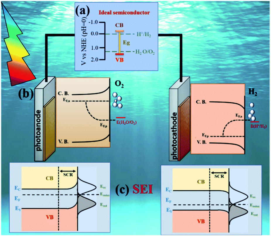 | ||
| Fig. 1 Schematic of the main design aspects for a PEC design: (a) semiconductor properties, including band gap (Eg), band position edges and chemical stability; (b) energetics diagram for water photoelectrolysis during illumination. The quasi Fermi levels (EF,n and EF,p) of the materials must be located above and below the water redox potentials for n-type and p type semiconductors respectively and (c) semiconductor electrolyte interface, influenced by the band bending and film structure. Adapted with permission from ref. 36 and 37. Copyright 2006, Elsevier and 2016, American Chemical Society. | ||
When a PEC cell is illuminated, electrons located in the semiconductor valence band (VB) are excited and promoted into the conduction band (CB) of the photocatalyst. A portion of these hole (h+)–electron (e−) pairs recombines, while another fraction is separated. After the separation is achieved, the electrons are collected by the back contact while the holes migrate to the photoanode surface to evolve the oxygen evolution reaction (OER); this phenomenon can be observed for the photocathodes in which the holes are collected while electrons are transferred to the interface to carry out the hydrogen evolution reaction (HER); when both are interconnected oxidation and reduction can be done simultaneously and can utilize light energy more efficiently. The mechanism will be explained in detail later in this section.
The eqn (1)–(3) show that the water splitting reaction require at least 1.23 V to take place, equivalent to 1.23 eV which is the theoretical minimum energy for this redox process. In order to accomplish this requirement, the semiconductor band gap (Eg) must be larger than 1.23 eV but it needs to be small enough to absorb the major part of the solar spectrum, being the ideal value around 1.6–2.0 eV.30–32 It is important to mention that even if the semiconductor is capable to absorb efficiently sunlight, the band edge energies need to be positioned correctly to preference the OER and HER.
| 2H2O + 4h+ → O2 + 4H+ (OER) | (1) |
| 2H+ + 2e− → H2 (HER) | (2) |
| 2H2O → O2 + 2H2 Eredox = 1.23 V | (3) |
Ideally, the CB must be placed at higher energy than the HER potential while the VB must be located at lower energy than the OER potential; Fig. 1a describes the ideal band diagram of a semiconductor capable to split the water molecule. If both requirements are fulfilled, when the semiconductor is illuminated, it will absorb photons and electrons will be promoted from the VB to the CB to achieve the water splitting reaction at the interface.
Despite the fact that the semiconductor properties dictate their potential use in efficient solar water splitting PEC system, as the photoelectrodes are immersed in water, it is imperative to comprehend the thermodynamic and kinetic parameters involved in the solid–liquid junction which is created by the interaction between the semiconductor and the electrolyte, known as semiconductor–electrolyte interface (SEI). When the electrode is immersed into an electrolyte solution, charge transfer reactions occur until thermodynamic equilibrium is reached and the Fermi level energy (Ef) of the semiconductor equals to the electrolyte redox potential.
At this moment, a charged interface is created, resulting in a potential drop at both semiconductor and electrolyte solution.
The Ef position with respect to the solution redox energy depends on the work function and excess positive or negative charge associated with the semiconductor electrode. In equilibrium, the band bending in case of n-type semiconductors results from an excess of positively charged donors resulting in an “upward” band bending, which is compensated by anion accumulation in the electrolyte solution at the surface. An opposite situation is observed in p-type semiconductors, where the Ef is below the redox potential of the electrolyte, implying a “downward” band bending32–34 as observed in Fig. 1c. The region where a band bending exists is known as space charge region (SCR) and its depth depends on the donor (acceptor) density, the semiconductor dielectric properties and the electric field. The flat band potential (Efb) is referred to the condition when a semiconductor in contact with another material is not polarized in the interfacial region. At this condition, the CB and VB are flat and no electric field acts on the charge carriers. More details about SEI and how the charge transfer processes at this interface are affected by film structure and preparation methods can be found elsewhere.32,35 It is important to note that the described phenomena occur under dark conditions; if the cell is illuminated, light induced processes will take place, and the electrode/electrolyte dynamics will be modified.
Under illumination, electron–hole pairs are photogenerated in the semiconductor. If the process is operated under open circuit conditions, the Ef increases due to the internal photovoltage. This process interrupts the thermodynamic equilibrium in the depletion region previously produced under dark conditions and the creation of a quasi-Fermi energy level is necessary to describe the electrochemical potential of the photo-generated electrons and holes (Fig. 1b). Those levels can be calculated according to the following equations:
 | (4) |
 | (5) |
At low injection conditions, a change in the majority carrier concentration is not significant. The net current across the illuminated semiconductor/electrolyte interface is constituted by the current due to the reactions involving photogenerated minority carriers as well as majority carriers at the opposite side of the cell.
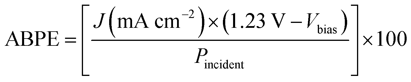
As explained previously, when the electrode is illuminated, charge carriers are photogenerated through light absorption. Due to the electric internal field generated at the semiconductor–electrolyte interface, the minority carriers are able to travel to the surface in a drift mechanism while the majority carriers diffuse to the bulk, process limited by the carrier diffusion length of the semiconductor. If carriers are generated in the bulk and the distance to the back contact is larger than the diffusion length, they will recombine. Charge carriers that are not lost by recombination, are transferred from the surface to the electrolyte, which is determined by thermodynamics and kinetics for charge transfer. To determine the efficiency of the system, it is necessary to employ the concept described by eqn (6). The applied bias photon-to-current efficiency (ABPE) is a parameter estimated from the current–potential curves under light condition as follows:
 | (6) |
Moreover, the incident photon-to-current efficiency (IPCE) is a measure of the ratio of the photocurrent versus the rate of incident photons as a function of wavelength:
 | (7) |
These two analyses, ABPE and IPCE, were proposed in literature as the most reliable way to compare performances of materials designed by different synthesis methodology.
Another alternative to calculate the total efficiency of solar radiant energy transformed into chemical hydrogen energy by a parameter known as solar to hydrogen efficiency (ηSTH), described by eqn (8):
 | (8) |
Over the past decades, effort has been devoted to design new materials or modify the existing materials to increase PEC device efficiency as described by these equations. Despite certain progress was reached, the predicted benchmark efficiency (over 10%) and stability for commercial application still far to be achieved. In recent years, graphene appeared as a promising material with positive impact when added during the fabrication of photoelectrodes. However, the role of graphene and how the properties are improved remain unclear. The next section will emphasize the main graphene properties which make it suitable for certain applications before introducing a discussion regarding its role in the photoelectrodes in PEC.
1.2 Graphene
Graphene is a metal-free material formed by a 2D carbon monolayer with a closely packed hexagonal lattice structure. Compared to graphite and carbon nanotubes, graphene exhibits much greater surface area and exceptional conductivity making it a potential candidate for different uses. Graphene has been reported in several applications such as a biosensors,38 gas sensors,8 electronic device design,39 transistors, fuel cells,40 photovoltaic devices,41 photocatalytic hydrogen generation, etc.Graphene is composed by sp2 hybridized carbons with a band gap nearly to zero. The electrical conductivity of graphene is related to its carbon network, which is 60 times higher than carbon nanotubes conductivity.39 Graphene also possesses a high density of surface-active sites and it is thermally stable.42,43 Contemplating its remarkable electron mobility, conductivity and stability, graphene is an excellent candidate to improve the efficiency of PEC systems. It has been shown that the insertion of graphene helps to improve the charge separation and increase the electrode surface area. In parallel, the new interface between the graphene and the semiconductor facilitates the hole/electron extraction, enhancing charge transfer reactions. Moreover, graphene, employed as a scaffold, creates a 2D conductive support path for charge transport and collection to enhance the electron transport properties of semiconductors.26,44
Since the graphene owns a higher work function compared to other semiconductors, it can act as an electron bridge to accelerate the electron transfer from the semiconductor CB to graphene, achieving a better charge separation.44,45 It is worth mentioning that some reports have demonstrated that chemical bond formation and the Schottky junction between the semiconductor and the graphene can modify the semiconductor band gap and enhance the light absorption.46,47
However, regardless of its benefits, graphene poor dispersibility significantly reduce its electrical conductivity, surface area, optical transparency and diminish the mass transfer kinetics.48–50 Due to this contrast, graphene derivatives represent an interesting and challenging field to be studied.
One of the main challenges in the synthesis and application of graphene sheets is to overcome the strong cohesive van der Waals energy of the p-stacked layers in graphite.51 Usually, graphene and its derivatives are synthesized via graphene oxide (GO) which can be obtained easily by graphite oxidation and subsequently exfoliation.52 GO consists of a graphene structure modified with different functional oxygen groups such as carboxylic, hydroxyl and epoxide which offer some attractive advantages for photoactive materials.50
Structurally, GO is an electronically hybrid material that features both conducting p states of sp2 carbon sites and a large bandgap between the s-states of its sp3-bonded carbons.53,54 This sp2/sp3 ratio can be modified by chemical reduction in order to produce reduced graphene oxide (rGO) which has brought the attention due to its remarkable conductivity and uniform incorporation in semiconductor electrodes. It has been proved that GO is able to drive the water splitting reaction by itself due to the band gap adjustment as a function of its oxidation degree.55 In fact, a recent work shows that an rGO/GO electrode achieves an enhanced response compared to GO, which the authors relate to the band gap tunning (displayed in Fig. 2), the faster electron acceptor capability of rGO and the electronic band structure of GO.56 Unfortunately, its response is still in order of microamperes and the system needs to be further studied.
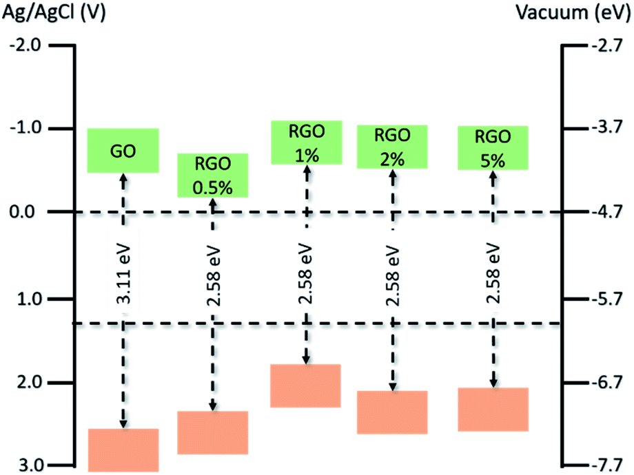 | ||
| Fig. 2 Energetic energy level diagram of rGO and GO/rGO electrodes at different GO wt%. The green and orange rectangles represent the CB and VB respectively. Adapted from ref. 56 with permission. Copyright 2019, Springer Nature. | ||
As modifier, rGO offers a distinct advantage of being chemically obtained through the cheap, simple and well-established Hummer method compared to pure SLG, which is synthesized by chemical vapor deposition (CVD) technique, a more expensive method. Different reports have shown that rGO improves the optical, conductive, and chemical properties of different photoanodes and photocathodes.
Another graphene derivate that is drawing a lot of attention are the graphene quantum dots (GQDs). The quantum-confinement and edge effects28,57 associated with their particle size, usually less than 10 nm, provide highly active reaction sites at the electrode. Additionally, GQDs have demonstrated excellent chemical stability, low cytotoxicity and high luminescence.28 One of the main advantages of GQDs is related to their electronic structure which can be modulated according to the particle size, conjugating them with polyaromatic rings to enlarge the π-conjugated sp2-carbon network or by introducing an intermediate n-orbital between π and π* orbitals via functionalization with electron-donating chemical groups.58 It has been shown that GQDs modification in TiO2 electrodes decreases the system impedance and improves the charge transport kinetics.57 Indeed, in some cases GQDs have been employed to tune the band gap to enhance the light absorption in the visible spectrum.59
In contrast, the use of overlayers and underlayers to improve the charge carrier dynamics is a solid strategy that has been largely explored. The deposition of a single layer of graphene (SLG) has shown better properties than rGO or amorphous carbon for PEC applications. Due its transparency, SLG only absorbs 2% of the solar spectrum, not interfering with the electrode absorption. Moreover, this layer conserves the high mobility of the charge carriers in graphene.60,61 Furthermore, SLG is chemically inert in air and in electrochemical media.62,63 As other graphene derivatives, the SLG has demonstrated an intrinsic photoresponse.
Although all aforementioned, each photoelectrode material presents unique properties and characteristics that need to be analysed in detail prior graphene incorporation to maximize its efficiency. The next sections disclosure the performance of graphene/semiconductor photoelectrodes supported by different studies published in the last five years.
2 Metal oxides/graphene
For PEC applications, metal oxides semiconductors offer many advantages as photoelectrodes. When used as photoanodes, they are not susceptible to oxidation reactions. Additionally, the wide Eg range of these semiconductors brings the possibility of being used as absorber to arise higher efficiencies. In terms of costs, most of metal oxides are composed by earth abundant elements which make their fabrication affordable. Unfortunately, one of the main limitations is associated to their relatively poor carrier kinetics which is reflected on the photoelectrode performance. Over the last decades, several efforts have been focused on creating new methodologies for produce stable and efficient photoanodes/photocathodes. Recently graphene (and its derivatives) started to be considered an attractive material to incorporate into metal oxides systems to evolve the HER and OER reactions.In this section, the recent developments of graphene/metal oxides as photoelectrode materials for water splitting will be highlighted. The graphene influence on the metal oxide photoanodes, photocathodes and heterojunction photoelectrodes reflected in different aspects (structurally, charge carrier dynamics and stability) during the water splitting process will be described as discussed in this section.
2.1 Photoanodes
Despite possessing unique and promising properties for water oxidation, many of metal oxides present intrinsic drawbacks64 that preclude their use as photoanodes by not reaching their maximum photocurrent density.64,65 It is noted that the key limiting factor of the poor PEC performance of many metal oxides is the high recombination rate of the charge carriers. Key strategies to address improvements for their use as stable and efficient photoanodes have been devoted. Researchers seek to include SLG, rGO,66 nitrogen-doped graphene67 and zero-dimensional GQDs68 as catalysts and/or supports in a wide range of photoanodes. In this section, a brief description of different graphene-based materials and their use as a “metal-free” carbon electrocatalyst materials69 on metal oxide photoanodes will be presented. Table 1 summarizes the most recent reports using graphene and its derivatives as a modifier in semiconductors for photoanode application.| Photoanode | Graphene derivative | Method for deposition | J (mA cm−2) | Measured potential | Electrolyte | Year (ref.) |
|---|---|---|---|---|---|---|
| a Photocurrent value in the range of nA cm−2. | ||||||
| Mo:BiVO4/G | rGO | Doctor blading | 8.51 | 1.23 VRHE | 0.1 M Na2SO4 | 2019 (ref. 80) |
| BiVO4/G/LDH | rGO | Electrodeposition | 1.13 | 1.23 VRHE | KPi (pH 7) | 2019 (ref. 79) |
| BiVO4/G/LDH | rGO | Hydrothermal | 2.13 | 1.23 VRHE | 0.1 M KPi | 2017 (ref. 92) |
| BiVO4/G | rGO | Drop casting | 0.13 | 0.8 VAg/AgCl | 0.1 M Na2SO4 | 2018 (ref. 93) |
| BiVO4/G | rGO | Drop casting | 0.55 | 1.2 VAg/AgCl | 0.1 M Na2SO4 | 2018 (ref. 94) |
| BiVO4/G/NiFe | rGO | Spin coating | 1.30 | 1.23 VRHE | 0.5 M Na2SO4 | 2018 (ref. 95) |
| BiVO4/G/Co-Pi | GQDs | Electrophoresis | 3.01 | 0.6 VRHE | 0.1 M KPi | 2019 (ref. 87) |
| BiVO4/LDH/G/CoPO3 | pGO | Spin coating | 4.45 | 1.2 VRHE | 1 M potassium borate | 2018 (ref. 96) |
| Co–N/P-GC-G/Fe2O3 | Flexible exfoliated graphene | Spin coating | 2.15 | 1.23 VRHE | 1 M KOH | 2017 (ref. 97) |
| Fe2O3/G | SLG | CVD | 0.75 | 1.23 VRHE | 1 M NaOH | 2018 (ref. 74) |
| Fe2O3/G | rGO | Dip coating | 0.88 | 1.23 VRHE | 1 M NaOH | 2017 (ref. 98) |
| Fe2O3/G | SLG | CVD | 1.64 | 1.23 VRHE | 1 M NaOH | 2019 (ref. 70) |
| FeNiOOH/Fe2O3/G | Nanocarbon | Spray-coating | ∼2.0 | 1.45 VRHE | 1 M NaOH | 2020 (ref. 99) |
| Fe2O3/G/Ag | rGO | Hydrothermal | 0.72 | 1.23 VRHE | 1 M KOH | 2018 (ref. 100) |
| Ag–TiO2/G | rGO | Anodization | 0.98 | 1 VAg/AgCl | 0.5 M Na2SO4 | 2019 (ref. 76) |
| TiO2–G | rGO | Drop casting | 1.44 | 1 VAg/AgCl | 1 M KOH | 2017 (ref. 101) |
| TiO2/G | GQDs | Spin coating | 6.35 | 0.5 VAg/AgCl | 0.1 M Na2S | 2017 (ref. 88) |
| TiO2/G | SNGQDs | Spin coating | 0.85 | 0.5 VAg/AgCl | 1 M Na2SO4 | 2018 (ref. 85) |
| TiO2@Ag/G | GQDs | Layer-by-layer | ∼0.6 | 1 VAg/AgCl | 0.5 M Na2SO4 | 2018 (ref. 102) |
| S–TiO2/G | S-doped rGO | Drop casting | 3.36 | 1 VAg/AgCl | 1 M KOH | 2018 (ref. 86) |
| TiO2/G | GQDs | Spin coating | 0.26 | 1.23 V RHE | 0.5 M Na2SO4 | 2020 (ref. 103) |
| ZnO NWs/G | N-doped GQDs | Layer-by-layer assembly | 0.6 | 1.0 VAg/AgCl | 0.5 M Na2SO4 | 2016 (ref. 104) |
| ZnO/G | rGO | Electrochemical reduction | 1.8 | 0.7 VAg/AgCl | 0.1 M KOH | 2017 (ref. 105) |
| ZnO | rGO | Sol–gel dip coating | 1.02 | 1.5 VAg/AgCl | 0.5 M Na2SO4 | 2018 (ref. 106) |
| WO3/G | rGO | Doctor blading | 2.85 | 0.6 VAg/AgCl | 0.5 M Na2SO4 | 2017 (ref. 107) |
| CSA–PANI–WO3/G | rGO | Spin coating | 1.54 | 1.23 VRHE | 0.1 M Na2SO4 | 2020 (ref. 108) |
| WO3/silane/G | GO | Dip coating | 1.25 | 1.23 VRHE | 0.5 M Na2SO4 | 2018 (ref. 109) |
| WO3/G | rGO | Hydrothermal | 750a | 0 VSCE | 0.05 M Na2SO4 | 2019 (ref. 110) |
The incorporation of graphene with no or negligible defects in the form of a large area sheet is highly required to maintain or enhance its electrical conductivity, electron mobility and carrier density.70 In this way, SLG has high transparency (97.7%) at visible light (λ = 550 nm); the Fermi level band alignment between SLG and the photoactive material makes it convenient for use in photoelectrochemical applications.71 It is expected that the SLG presence would not lead to a change in the photoanode optical properties due to its very thin layer and high transparency.72 Since α-Fe2O3 typically suffer from undesirable surface states,73 the addition of SLG as a passivation layer leads to an impressive improvement in the PEC performance of hematite photoanodes. The passivation effect of the surface states after SLG incorporation on the top of the photoanode, resulted in an increased lifetime of the photogenerated holes.70 Additionally, as a consequence of the strong interaction between SLG and the photoanode, it was observed an efficient charge carrier separation and better hole accumulation at the photoanode surface,70,74 increasing the water oxidation efficiency.70 Although much higher photocurrent can be obtained after the deposition of SLG on the top of metal-oxides films, it is important to highlight that in this case different methods for SLG deposition should be taken into account for better interaction of the semiconductor with the graphene material, in such a way that not only the photoanode surface would be benefited by the SLG presence, but the whole composite.
Differently of SLG, the reduced graphene oxide (rGO) can lead to a significant improvement in the light absorption upon its addition on photoelectrocatalyst system. In this trend, the incorporation of rGO has been widely explored.66 It has been shown that when incorporated, rGO can broaden the absorption spectrum of many metal oxides that poorly absorb visible light.75 In general, it has been discussed that this may occur due to the orthogonalization of light in porous structure of carbon materials. The high porosity of rGO-based materials can lead to multiple reflection of light inside the film, improving the light absorption.76,77
The two-dimensional rGO nanosheets present high electron mobility and π-electron conjugation.78 Besides the light absorbance improvements, owing to its excellent electronic properties, the presence of rGO on top of the photoanodes can lead to an increase of the charge separation efficiency. As a consequence, a lower bulk recombination is obtained, which makes rGO as an effective electron capturing and transferring material.79,80 The onset potential shift suggest that the role of rGO is to increase the carrier transport and electron collection efficiency.
The application of rGO with plasmonic nanoparticles in order to enhance the PEC performance of conventional semiconductors has also been reported,76 in which a portion of hot electrons generated in metal nanoparticles can be accepted and shuttled via rGO sheets either by UV or visible light, minimizing charge recombination. Despite the incorporation of rGO has provided excellent improvements in photocurrent density of many graphene-based photoanodes, this material still contains a considerable amount of heteroatoms,81 as well as an incomplete restoration of a perfect carbon lattice,82 turning other graphene derivatives more attractive.
Besides the simple addition of graphene aiming better PEC performances by passivation effect, another approach is to make graphene properties tuneable.83 Graphene electronic properties can be tuned by doping it with heteroatoms, opening a new venue to further improve the performance of the metal oxides.84 By reacting epoxy, hydroxyl and carbonyl groups present in the rGO with molecules containing heteroatoms like N, P and S, these atoms can replace some of the carbon sites in the graphene framework structure, introducing defects. These intentionally added defects lead to improved chemical stability, as well as surface area and electron transfer.84,85 By doping with heteroatoms, the doped-graphene material can be tailored to act as electron donor or acceptor, depending on the electronegativity of the dopant with respect to carbon atoms. Such defects are responsible for opening the Eg in graphene-based materials, offering additional fine tuning of the band alignment.
In this context, it has been shown that sulfur doping greatly broad the photoanode light absorption.86 The efficient visible light harvesting resulted in the improvement in photocurrent density. The enhancement was attributed to the increased separation rate of electron–hole pairs as well as electron transfer at the surface, leading to a strongly chemical coupling. As consequence, a negative shift in the onset potential which was attributed to the negatively shifted Fermi level was noticed. The resulted positively charged carbon atoms turned them able to adsorb OH− species, resulting the more favourable O2 evolution at the photoanode surface.
Since the photocurrent density is described as a function of the absorbed photocurrent (Jabs), efficiency of charge carrier separation (ηsep) and injection (ηinj), different types of graphene derivatives can lead to different PEC behaviours.90 This trend can be simplified in the following equation:
| JPEC = Jabs × ηsep × ηinj | (9) |
For instance, a certain method for graphene deposition targeting to enhance light absorption can lead to higher Jabs values, however, by increasing the film thickness, recombination sites can be formed at the grain boundaries or at multiple layers and consequently, ηsep and ηinj values may be negatively affected.
It is worth mentioning that the architecture of the metal oxide in contact with graphene is equally important, leading to worse or better physicochemical interaction between the materials. In this circumstance,89 some nanostructured photoanodes (exemplified in Fig. 3g–m) decorated with rGO has shown an outstanding response related to the improved light absorption which activated the OER.89 In these cases, nanostructures serve as high-speed transport path for photogenerated electrons and a light absorber while rGO acts as electron conduction and surface passivation layer. Consequently, an enhancement of Jabs and ηsep parameters contribute to improve the overall photocurrent density.
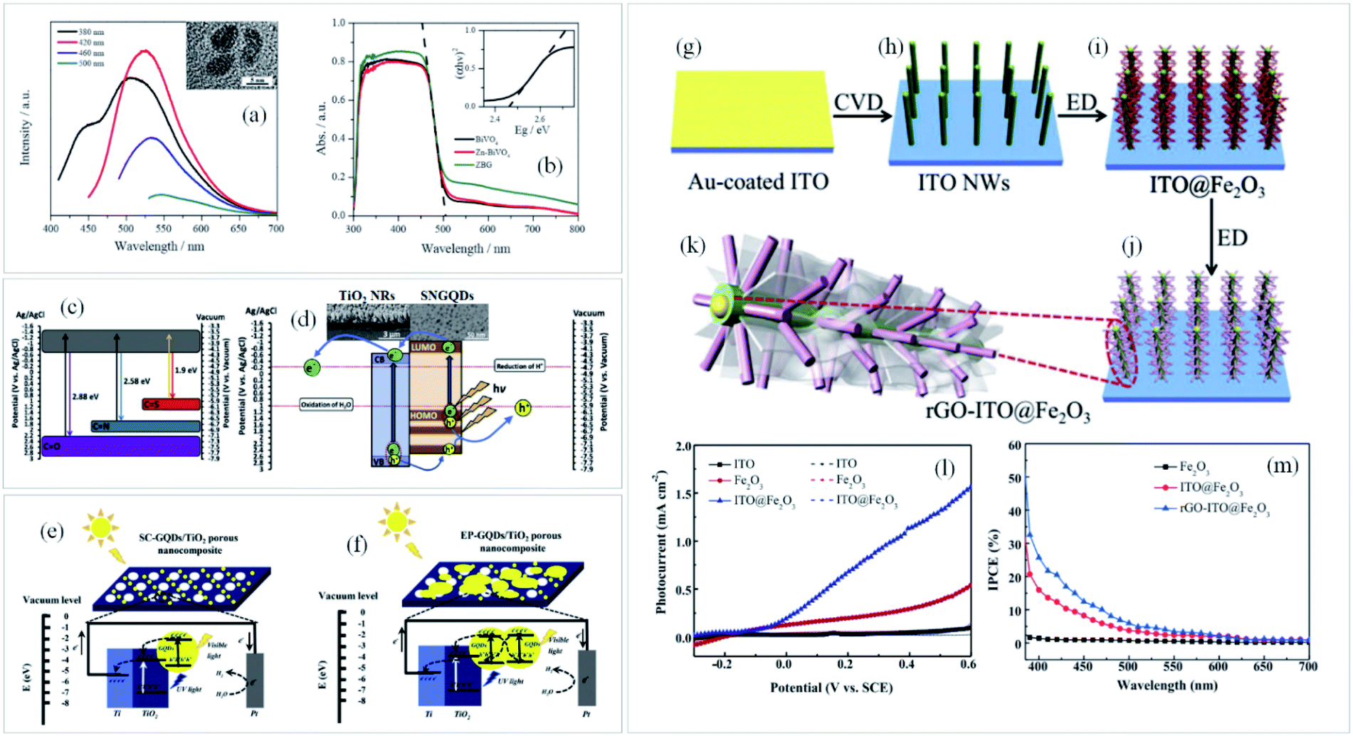 | ||
| Fig. 3 (a) PL emission spectra of GQDs at the excitation wavelength from 380 to 500 nm with their respective TEM images and the (b) UV-Vis spectra of BiVO4, Zn–BiVO4 and Zn-doped BiVO4/GQDs (ZBG). Reprinted with permission from ref. 87 Copyright 2019, Elsevier. (c) Energy levels of SNGQDs related to doping of oxygen, nitrogen and sulfur atoms and (d) energy diagram depicting charge transfer between TiO2 and SNGQDs. Reprinted with permission from ref. 85 Copyright 2018, Elsevier. Proposed mechanism for PEC water splitting by (e) spin-coated and (f) electrodeposited GQDs/TiO2 photoanodes. Reprinted with permission from ref. 88 Copyright 2017, Elsevier. Schematic illustration of (g–k) rGO-ITO@Fe2O3 photoanode fabrication process, (l) photocurrent density × applied potential and (m) IPCE plots of ITO, ITO@Fe2O3 and rGO-ITO@Fe2O3 photoanodes. Reprinted with permission from ref. 89 Copyright 2016, Elsevier. | ||
Another interesting graphene derivative for this approach is the use of GQDs, which are mono or few-layer graphene sheets with lateral dimensions of less than 100 nm.68 Their unique properties such as excellent up-conversion, quantum confinement with size dependent photoluminescence (PL), high aqueous solubility, robust chemical inertness and low cytotoxicity91 open up new avenues and shed light on a novel branch of advanced nanostructured materials for solar-driven water splitting. For instance, by modulating the emission wavelength of the GQDs and matching it with the absorption edge of the semiconductor (Fig. 3a and b), both light harvesting and IPCE can be greatly improved.87
Doping graphene quantum dots with sulfur or nitrogen (SNGQDs) can input novel valuable properties to graphene-based materials. By co-doping them with different atoms, SNGQDs can originate two or more excitation wavelength-independent PL and broad the absorption in the visible region of light with multiple absorption edges,85 turning them auspicious photosensitizers for effective PEC applications. Depending on the doping atom, different energy levels of the SNGQDs (Fig. 3c) can be obtained leading to better alignment with the oxidation and reduction energy levels of water splitting reaction (Fig. 3d).
Interestingly, it has been shown that depending on the deposition method, GQDs can also play different roles in the photoanode performance. For instance, authors employed two different methods88 to deposit GQDs on TiO2 photoanodes, which led to a considerable difference in charge transfer and PEC performance. By using spin coating as deposition method, GQDs behave as a photosensitizer donating electrons to the CB of the semiconductor. On the other hand, if the amount of GQDs deposited on a specific photoelectrode is not well controlled, as occurred when deposited by electrodeposition, their excess causes blockage of electron transfer, in a way that instead of facilitating electron transfer to the semiconductor conduction band (Fig. 3e), the photogenerated electrons in the GQDs obtain more probability to be recombined with holes (Fig. 3f).
This section described a wide range of properties enhanced by the addition of graphene-based materials on metal oxide photoanodes. We note that the key limiting factor of the poor PEC performance of many metal oxides is the high recombination rate of the charge carriers. Despite such improvements have been achieved, many questions are still opened. We believe that further studies using appropriate techniques to improve the understanding of the real role of graphene on the enhancement of photoanodes efficiencies towards water splitting are very important. Generally, it has been reported that when incorporated onto metal oxide photoanodes, graphene acts improving light absorption and charge transfer, which led to a decrease in the charge recombination rate at the semiconductor/electrolyte interface, enhancing the PEC performance.
Graphene and its derivatives lead to a wide range of photocurrent density, varying from μA to mA cm−2, and their performances may be related to the quality of the synthesized material as well as the method for preparation and deposition. Most of the papers describing the incorporation of graphene as an electrocatalyst, use rGO as the main material, and the reason relies in the facility to synthesize it, being a versatile platform for many different composites. In general, two main properties are observed to be enhanced after the incorporation of graphene and its derivatives on different metal oxide photoanodes, the light absorption and the charge transfer. All the others described, as photogenerated holes lifetime, charge separation and photostability, can be interpreted as a consequence of them.
2.2 Oxide-based photocathodes
In a photoelectrochemical cell, photocathodes must provide enough cathodic current to reduce protons and produce H2 in a stable aqueous environment.111 Even if PEC water reduction is energetically more favourable against water oxidation reaction, finding a suitable and electrochemically stable material to evolve the water reduction represent a more difficult task. For this reason, the available reports of oxide semiconductors as photocathodes are limited compared to photoanodes studies.Copper-based materials fulfill the basic requirements to act as photocathode with special attention in literature dedicated to compounds as CuO,112 Cu2O,113 CuBi2O4,12 CuFe2O4114 and Ca2Fe2O5.115 Despite the progress achieved, these materials suffer critical drawbacks such as photocorrosion leading to a poor material stability followed by some electronic limitations usually associated with fast charge recombination. To mitigate those common issues and further optimize the photocathode activity, several strategies have been employed, including graphene insertion in different facets. In this chapter, the effect of graphene insertion into metal oxide photocathodes focusing on electronic structure, charge carrier kinetics and stability will be revised accordingly to meet the consensus and contradictions in the literature.
As stated in the last section, graphene can modify different material properties depending on the deposition technique and the chosen derivative, but how this insertion affects the photocathode electronic structure? Some studies12,116–118 have shown by XPS and Raman that the graphene or rGO addition into Cu based photocathodes allow the formation of Cu–O–C bonds, indicating a superior interaction and interfacial charge transfer between graphene and Cu compounds which reduce the electron density around the Cu material. It is worth mentioning that in these cases, graphene-based materials have been synthesized separately and subsequently added into the electrode by methods such as spin coating, drop casting or impregnation. In contrast, different behaviour was observed when the graphene layer is added by CVD: XPS studies did not suggest any chemical interaction among graphene and Cu2O; due to the Cu2O porosity, the CVD layer could not fully cover all photocathode surface.119
Despite Cu–O–C bonds have been successfully demonstrated by some authors, optical measurements are primordial to understand the role of graphene and its derivatives into the photocathode electronic structure. Absorption measurements of photocathodes modified by graphene,116 rGO,117 and NGQDs120 indicated that this modification increases the absorption range of the nanocomposites in the visible region but, in all circumstances, the band gap analysis showed that graphene based materials have not been incorporated into the lattice. However, in cases when a higher concentration of graphene (or its derivatives) is added, a competition of light absorption between graphene and the semiconductor and light blocking effects12,116,121,122 are noticeable.
Furthermore, to overcome the main drawback faced by Cu-based photocathodes, the photocorrosion, diverse strategies such as the passivation layers, crystal structure/morphology modification and cocatalyst addition have been employed to improve stability. Considering this approach, photocathode modification with graphene-based materials116,118,119,121 demonstrated to be a promising strategy to avoid the electrode photocorrosion. Since graphene and its derivatives can act as electron acceptors, they suppress the redox activity of the copper-based oxides photocathodes. Fig. 4 summarizes the photocurrent stability obtained by chronoamperometry measurements reported which is defined as the photocurrent density measured at the end of the test (J) divided by the photocurrent density at t = 0 s (J0); it is observed that, in all systems, the stability improved significantly compared to the bare system. Some authors117–119 affirm that the synergistic interaction between graphene and Cu photocathodes inhibit the catalyst self photocorrosion as well as improved the photocurrent density.
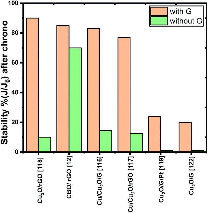 | ||
| Fig. 4 Stability percent of different systems before and after graphene (or graphene derivatives). All chronoamperometry measurements have been performed at 0 V vs. RHE at a given time. | ||
By analysing the stability (Fig. 4), two systems presented a lower enhancement (from 1% to ∼20%) when graphene is added; in both cases, graphene did not fully cover the Cu2O layer. For this reason, they deposited an additional layer of TiO2119 or amorphous molybdenum sulfide (a-MoSx)122 which improved the stability percent to 67% and 40% respectively. These studies bring the possibility of combining graphene with other semiconducting oxides to improve PEC systems. And in fact, the research in this field is pointing towards a combination of materials to succeeded in improved OER and HER reactions.
Although the chronoamperometric measurements have been performed at 0 V vs. RHE, the longest test data reported is 20 minutes which suggest the electrode photostability is not enough for scale-up. Even if several authors affirm that graphene electron mobility and its behaviour as electron acceptor boost the transfer of photogenerated electrons from photocathode to the electrolyte,12,116,121 it must be taken into account that Cu based materials by themselves can achieve remarkable performance during limited time and, for this reason, it is necessary to focus on resolve their stability drawbacks to then create strategies focused on charge transfer kinetics.
Despite all mentioned above provides valuable information to create new strategies for photocathode design, some issues are still elusive. Recently, Yu and collaborators123 determined that the GO modification on Cu2O/C/NiCoB films increases the photocathode surface area, suggesting that GO addition induce the formation of abundant catalytic sites facilitating the charge transfer during the water reduction reaction. Also, it is necessary to understand how the electrocatalytic effect of graphene and its derivates influences the charge carrier dynamics of the photocathodes which is observed in the J–V curves.118,120
Even if the quantity reported studies are still limited, the recent studies have demonstrated the importance of the graphene deposition technique; if an optimal deposition is achieved, graphene and its derivatives can create chemical bonds between the photocathode and their carbon network facilitating the charge carrier dynamics and the stability without blocking the photocathode light absorption. Although the clear improvement in the charge carrier dynamics that graphene brings to the photocathode performance, this fact is not fully understood and, in some cases, it is important to consider if graphene can be the best material to be used as passivation layer or can be combined with other semiconductors to enhance the metal oxide photocathode activity.
2.3 Heterojunctions
The possibility of improving the performance of water splitting photoelectrodes by the integration of two or more semiconductors with different optical and/or physical characteristics has been constantly reviewed.124–129 Several findings published to date confirm that drastic limitations of photoelectrodes, such as elevated charge carriers recombination rates and propensity of undergoing photocorrosion, can be mitigated by the proper connection of semiconductors, in which the formed intimate contact, referred as heterojunction, favours the spatial separation of photoexcited electrons and holes as a result of suitable band energy levels alignments.124,125,130–132 And in fact, we might consider that the combination of graphene with photoanodes and photocathodes discussed previously, is an heterojunction itself.Since effective heterojunctions drive electrons and holes in opposite directions, especially under the influence of an applied bias, they minimize the surface/interface charge accumulation that provokes photocorrosion. This electric field built across the framework intensifies the charge carriers migration, excelling the electron–hole separation and, consequently, reducing their recombination at specific points of the crystalline structure.124,133
In general, graphene and its derivatives are incorporated in photoelectrode heterojunctions as solid-state mediators to intensify the charge shuttle between the components, due to their aforementioned inherent electronic properties. Besides, owing to its high specific surface area, graphene contributes to the photoelectrocatalytic reactions, as it provides extra adsorption and catalytic sites.127,134
Among the graphene-related rational designs recently employed in heterostructured water splitting photoelectrodes, rGO is the most recurrent because it presents striking advantages over pure graphene and GQD, as mentioned before.125 Furthermore, compared to GO, rGO possess a reduced number of oxygen-containing groups that can act as deep recombination centres.
In fact, based on evidences from recent publications, this balanced content of pendent functional groups on the reduced graphene oxide layers is the responsible for the effective linking between the semiconductors in heterojunctioned photoelectrodes, resulting in the broader usage of rGO as mediator compared to the other graphene-like structures. As the connected semiconductors also contain reactive surface functional groups, they interact with those pendent on the rGO sheets, creating bonds that ensure an effective contact between the heterostructure components.
The lack of functional groups in pure graphene tends to preclude a stable and concomitant connection of the graphene sheets with two semiconductors that might possess very distinct surface properties. On the other side, non-reduced GO and graphene quantum dots have higher densities of these oxygenated functional groups. As these groups act as charge carrier trap centres, they may impair the charge transport within the layer and, consequently, the charge shuttle between the photocatalysts and the overall photocatalytic efficiency.89,125,134–136
As a consequence, most of the research investigations employ effective routes in which the connection of the semiconductors is guaranteed by their interaction with GO containing high density of oxygenated groups, followed by a reduction procedure to eliminate the excess of these recombination centres.
As a recent showcase, this strategy was adopted for a water splitting photoanode in which rGO was employed as the solid-state charge carrier mediator two oxide semiconductors (SC/rGO/SC).79,92,132,137–139 A clear example is schemed in Fig. 5a–c140 where it is noticeable that the addition of rGO had a paramount contribution to the activity of the photoanode, as the charge transfer at the graphene-free interface was hindered by recombination centres at the intrinsically discontinued heterojunction interface. In contact with the oxide semiconductor, rGO nanosheet creates a Schottky junction which favours the transport of charge carriers from one oxide semiconductor to the other, lessening the recombination of electron–hole pairs.125 Also, it has been suggested that graphene layer reduces the interfacial charge transfer resistance.141 Moreover, some authors affirms that rGO tune the electrical connection between both semiconductors.142
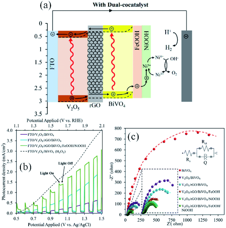 | ||
| Fig. 5 The application of rGO as the charge carrier mediator in the V2O5/BiVO4 heterojunction. (a) The energy diagram depicting different components of the photoanode, including rGO layer; (b) photocurrent density versus applied potential curves and (c) Nyquist plots of EIS for the electrodes prepared in this study. Reprinted with permission from ref. 140 Copyright 2020, Elsevier. | ||
Heterojunctions formed by earth abundant non-oxide semiconductors can also be improved by the rGO incorporation as a bridged solid-state mediator, forming type II heterostructure.143–145
Especially for chalcogenides-based photoelectrodes, photoinstability is the primary disadvantage compared to metal oxides. Chalcogenides possess lower band gap values due to their energetic valence band edges, however their application as photoelectrodes is hindered by the strong photocorrosion tendency. This limitation can then be alleviated by a fast charge carriers extraction that might be accomplished by an adequate coupling with rGO.125,143,145,146 As an example, a substantial boost in the photocurrent was observed for the TiO2/rGO/MoS2 photocathode (Fig. 6a) compared to the binary TiO2/rGO and TiO2/MoS2 systems. A similar behaviour is observed in the Nyquist plots (Fig. 6b), which indicate that the charge transport resistance is much lower for TiO2/rGO/MoS2.144 An interesting point of debate raised by this work is that only a slight activity improvement took place when the single TiO2 film was solely wrapped by rGO layers due to the blockage of the TiO2 active sites for water reduction by rGO indicating its poor activity as cocatalyst. On the other hand, extra catalytically active sites are included by the attachment of MoS2 to the TiO2/rGO electrode, while rGO guarantees the efficient charge transfer between TiO2 and MoS2 (Fig. 6c).
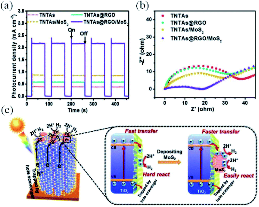 | ||
| Fig. 6 Results set for a ternary system containing MoS2 immobilized on a rGO-wrapped TiO2 nanotube array, applied as an efficient photoelectrode for water splitting. (a) Transient photocurrent responses, (b) EIS Nyquist plots of the prepared devices, and (c) schematic energy diagrams depicting the charge transfer dynamics of the photoelectrode under operation. Reprinted with permission from ref. 144 Copyright 2018, Wiley-VCH. | ||
This study highlights the importance of a following a rational design for the addition of graphene layers in a photoelectrode, as they may occlude important catalyst sites. An erroneous approach might offset the benefits brought by graphene in the charge transfer/separation.
By developing a different configuration for the inclusion of rGO in a type II heterojunction, Hou and co-workers137 were able to achieve an impressive photocurrent enhancement for a ZnO/Cu2O heterostructure from 3.22 to 10.11 mA cm−2 at 1.23 VRHE (AM 1.5G). To design the photoelectrode, an intimate contact between ZnO nanorods (NRs) and Cu2O nanocubes was created, then rGO sheets wrapped the whole set as cocatalyst (Fig. 7a and b). The authors proposed that rGO sheets are responsible for the direct transport of photoexcited electrons from the heterojunction to the substrate. Due to its higher work function, rGO promoted directional electron transfer by forming Schottky junctions with both semiconductors.125 Meanwhile, the photoholes generated at ZnO are injected into Cu2O, inducing an effective electron–hole separation. These inferences are represented by the energy diagram in Fig. 7c.125,143
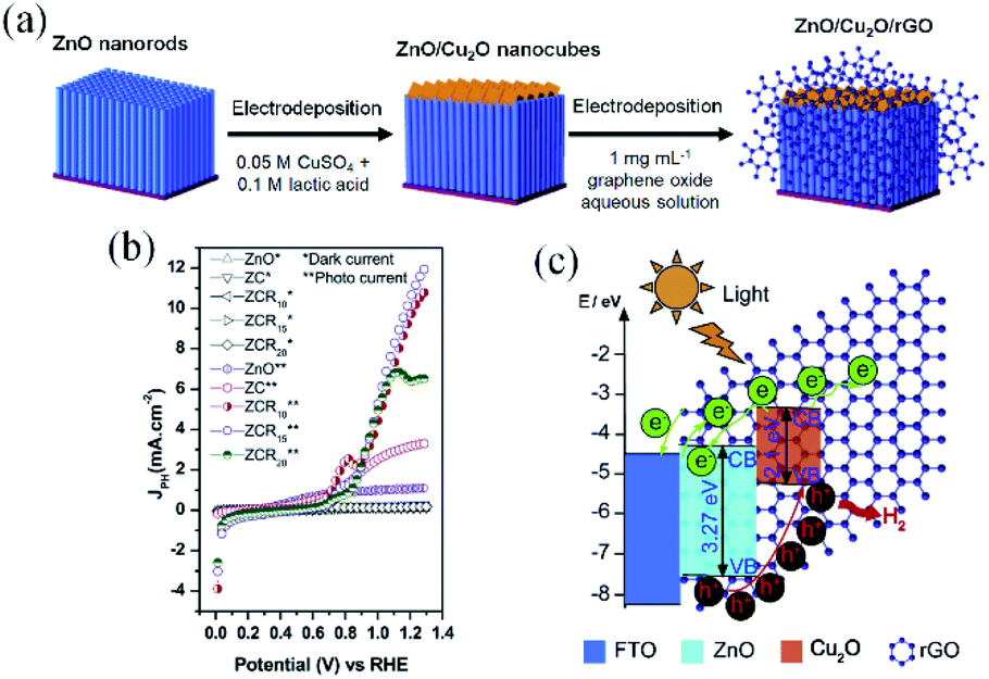 | ||
| Fig. 7 Results and schemes describing the synthesis and energy diagram of the ZnO/Cu2O/rGO heterostructured photoelectrode. (a) Scheme depicting the steps used for the photoelectrode preparation, (b) linear sweep voltammetry and (c) schematic energy diagram representing the charge mobility within the heterostructures under water splitting operation. Reprinted with permission from ref. 137 Copyright 2019, Elsevier. | ||
It is clear that the performance improvement achieved in this case results from a combination of the high crystallinity of the ZnO and Cu2O building blocks, the broad light absorption by Cu2O and the electric field induced by the p–n junction. However, rGO incorporation has a key role in the efficiency, as besides favoring a faster charge carrier diffusion, it acts in the passivation of Cu2O nanocubes, by preventing the direct contact with the electrolyte. Once again, it is important to highlight that the strong bonding between the semiconductors and rGO provided by the electroreduction method was of paramount importance for the performance and stability achieved for this photoelectrode. Additionally, rGO layer improves the Cu2O stability as discussed in Section 2.2 where it was observed that the wrapping graphene layers can also passivate the electrode by preventing the direct contact of Cu2O with the electrolyte.129,137,138,147
In summary, it has been demonstrated by the available literature that the photoelectrocatalytic performance of heterostructured photoelectrodes for water splitting can be enhanced by the incorporation of graphene at specific interfaces. As a rule of thumb, the substantial improvements observed in all cases are related to the high electrical conductivity of graphene sheets, which improve the charge carriers transfer across the heterojunction components.
Nonetheless, graphene-like species containing appropriate functional groups may strengthen the interfacial contact between semiconductors and increase the surface phase junction area, as it extends the interface between the semiconductors, intensifying the charge exchange.141 The photostability improvements of heterojunctions containing Cu2O and chalcogenides by the incorporation of graphene-like structures have also been reported. In all cases, the 2D network works as a rapid channel for the charge carriers transport, preventing charge accumulation at the unstable semiconductors.79,144,148,149
Some other points must be taken into account to further collect positive outcomes from the graphene-containing heterostructured photoelectrodes. The concomitant connection of the 2D sheets with both semiconductors is one important parameter that must be studied. This is a critical point that will affect the photoelectrode performance and stability, especially because of the harsh conditions usually used in the photoelectrochemical reactions. Thus, the composition and surface properties of the binding semiconductors must have good affinity with the functional groups pendent to the graphene-like sheets to ensure effective electronic contacts.
Apparently, reduced graphene oxide has been used in the great majority of the PEC heterojunctions due to the available oxygenated functional groups – such as carboxyl, hydroxyl and epoxy groups – that act as binding sites for the interaction with the reactive surface groups of the semiconductors that are connected.136 These features allow the creation of effective interfaces under mild synthetic conditions, such as the electrochemical reduction of GO, which was the method employed by most of the studies exposed in this review. Moreover, the electrical properties of rGO are tunable and adequate modifications might enhance the connectivity with another semiconductor surface to form heterojunctions.
Fig. 8 exhibits the best photocurrent performance reported the last years oxides photoelectrodes modified with graphene. It can be noticed that even if graphene improves material stability, the photocurrent response is not close from the theoretical values or Cu2O best response (∼10 mA cm−2)150 where, additional to a protective layer, the formation of p–n junction and a cocatalyst deposition were indispensable for raising a promising performance.
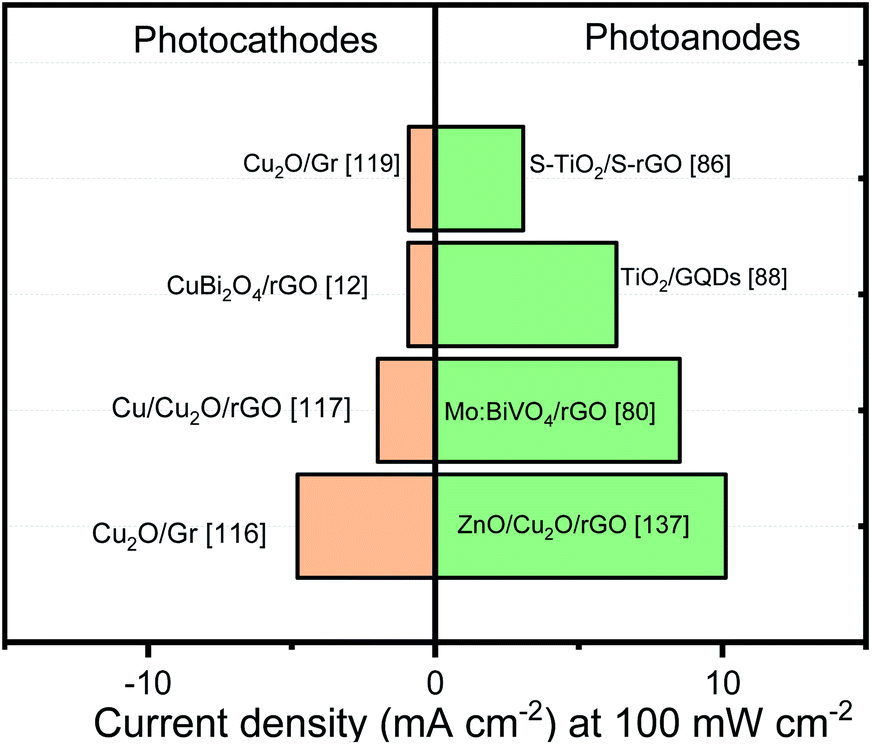 | ||
| Fig. 8 Photocurrent benchmark of graphene/oxides photoelectrodes. Data were extracted from various reports in the literature. | ||
In case of the photoanodes, the incorporation of rGO into different systems has shown the best results. The photocurrent values obtained by the rGO/heterojunction represent a good strategy to optimize the photoanodes. In contrast, although Mo:BiVO4/rGO nanocomposite performance can be interesting, the photocurrent values obtained by other methodologies are close from this benchmark.
Despite impressive photocurrent values have been obtained by the addition of many types of graphene and its derivatives in metal oxide semiconductors, the nature of the active sites remains elusive, leading to a superfluous comprehension of the role of the graphene. Therefore, future challenges should bring together in situ or operando with advanced techniques to amplify the comprehension of the mechanisms and species involved.
3 Non-oxide semiconductors/graphene
Non-oxide semiconductors are considered as attractive candidates for PEC solar fuel production due to their small band gap which permits capturing a wide range of the solar spectrum. Materials such as transition metal sulfides, selenides or silicon based photoelectrodes have been explored to evolve the OER or HER by themselves or combined with other semiconductors. However, during operation, few drawbacks associated with their physical, chemical and electronic properties have inhibited their performance to obtain high efficiencies. In this sense, graphene incorporation has been employed to overcome the problems associated with chemical and PEC corrosion, charge transport and separation deficits with remarkable results. In this section, the influence of graphene (and its derivatives) insertion on the PEC performance of non-oxide semiconductors in the past 5 years will be summarized. Due to the extensive nature of the non-oxide semiconductors and their peculiarities, this section has been further divided according their chemical structure.3.1 Graphene-based transition metal chalcogenides (TMCs)
Transition metal chalcogenides (TMCs) are normally considered potential candidates for PEC water splitting. The VB of TMCs normally consists of 3p orbitals of S (or Se), which result in a more negative VB and a narrower Eg compared to metal oxides.151 However, the PEC performance using TMCs-based as photoelectrodes is still limited because of the fast charge carrier recombination. In addition, photocorrosion is actually a common problem for most TMCs.152 Besides a plethora of morphologies (e.g. nanowires,153 NRs154,155 and nanoflowers154), introduction of noble metal nanoparticles (e.g. Pt156 and Au157), formation of heterojunctions (e.g. TiO2/CdS158 and CdS/MoS2 (ref. 159)), the incorporation of graphene and/or its derivatives has also been widely used to improve electronic transport and decrease carrier recombination in these semiconductors. In order to gain a deeper understanding of the graphene-based TMCs, this section has been divided to analyze the binary transition metal sulfides, two-dimensional metal sulfides and ternary transition metal sulfides and selenides.Due to its band gap, CdS been combined with wide band gap semiconductors (e.g. TiO2 and ZnO) to extend the absorption edge into visible light region and improve photoelectrochemical activity.164,165 As observed for metal oxide heterojunctions, graphene sheets (and its derivatives) can also be wrapped between two semiconductors to achieve better charge separation. Several reports155,166–168 have shown that a graphene interlayer (mostly rGO) between the semiconductor leads a photocurrent density improvement associated with a decrease in the recombination. However, as CdS acts as absorber layer and it is directly exposed to the electrolyte solution, the photocurrent decay of the systems can be related to Cd photocorrosion which has not been addressed by the authors.
For wide band gap transition metal sulfide semiconductors, graphene and its derivatives can also improve photogenerated carrier separation and transport. Zinc sulfide (ZnS) is a wide band gap semiconductor (Eg = 3.6 eV), which means that it cannot be photoexcited by visible light irradiation. A particular case where rGO is used as support for the growth of ZnS/Cd NRs open the possibility of designing new organized heterojunctions with attractive properties.156 Additionally to the photocurrent improvement associated with graphene as charge transfer mediator,158,160,169 the ZnS role as charge collector and the CdS absorption capability, the authors could not reproduce a similar pattern on the heterojunction without rGO addition.
Table 2 shows some examples of others photoelectrodes based on binary transition metal sulfides and graphene (or its derivatives) with their respective PEC performance. We can observe that there is a trend in the literature to synthesize graphene-based TMCs nanocomposites using chemical methods such as hydrothermal and solvothermal methods. Generally, these one-step methods require low-cost and simple equipment (e.g. autoclave and an oven) and can achieve a high-yield and large-scale production. During the hydrothermal synthesis, the GO, employed as precursor, is reduced into the reactor to obtain rGO which usually present structural defects, such as vacancies, heptagon and pentagon rings, edge effects and residual functional groups.179 Although these defects significantly affect electronic and chemical properties of the rGO sheets, the recent reports (Table 2) showed that this low cost methodology allows to design interesting heterostructures with higher photoresponses compared to other sophisticated methodologies needed to deposit graphene. On the other hand, the chemical methods permit to control several important experimental parameters. Consequently, a better interaction and control over the size and shape distributions of TMCs nanoparticles on the rGO sheets can also be obtained.66
| Photoanodes | Preparation method | Substrate | Light source | Electrolyte | Applied potential | Photocurrent density | Year (ref.) |
|---|---|---|---|---|---|---|---|
| a Gr = graphene; rGH = rGO hydrogel; NPs = nanoparticles; NRs = nanorods; TNTs = titanate nanotubes; CoNHs = cobalt-based nanohybrids (Co3S4/CoS2); GCE = glass carbon electrode; CFP = carbon fiber paper; SILAR = successive ionic layer adsorption reaction. | |||||||
| Gr–CdS NPs | Chemical solution | FTO | 300 W Xe arc lamp (100 mW cm−2) | 0.5 M Na2SO4 | 1.0 VRHE | 0.024 mA cm−2 | 2020 (ref. 170) |
| CdS NPs/N,S-co-doped rGO | Low temperature calcination | FTO | 300 W Xe arc lamp (λ ≥ 420 nm, 100 mW cm−2) | 0.5 M Na2SO4 | 0 VAg/AgCl | 0.010 mA cm−2 | 2018 (ref. 171) |
| CdS NPs/rGH | Hydrothermal | FTO | 500 W Xe arc lamp (320–780 nm, 80 mW cm−2) | 0.1 M Na2SO4 | 0 VSCE | 0.10 mA cm−2 | 2018 (ref. 172) |
| CdS QDs/GQDs/TNTs | Solvothermal, ion-exchange reaction and sulfurization | FTO | 300 W Xe arc lamp (λ ≥ 420 nm, 100 mW cm−2) | 0.1 M Na2SO4 | 0 VAg/AgCl | 0.045 mA cm−2 | 2020 (ref. 158) |
| CdS core/Gr/TiO2 shell | Hydrothermal | FTO | 150 W Xe arc lamp (AM 1.5G, 100 mW cm−2) | 0.1 M Na2S | 0 VAg/AgCl | 0.13 mA cm−2 | 2020 (ref. 173) |
| CdS NPs/NiS sheets/rGO | Solvothermal | FTO | 300 W Xe arc lamp (λ ≥ 420 nm, 100 mW cm−2) | 0.5 M Na2SO4 | 0 VAg/AgCl | ∼7.5 μA cm−2 | 2018 (ref. 167) |
| CdS–Sn2S3 clusters/rGO | Hydrothermal | GCE | 300 W Xe arc lamp (λ ≥ 420 nm, 100 mW cm−2) | 0.5 M Na2SO4 | 0 VAg/AgCl | 0.026 mA cm−2 | 2018 (ref. 168) |
| g-C3N4 NSs/CdS NRs/rGO | Wet-chemical | ITO | 300 W Xe arc lamp (λ ≥ 420 nm, 100 mW cm−2) | 0.1 M Na2SO4 | 0 VAg/AgCl | 0.38 μA cm−2 | 2017 (ref. 155) |
| ZnS nanospheres/rGO | Hydrothermal | GCE | 110 W Xe arc lamp (λ ≥ 420 nm, 100 mW cm−2) | 0.5 M Na2SO4 | 1.23 VRHE | 1.1 mA cm−2 | 2018 (ref. 174) |
| ZnS NRs/N-doped Gr | Hydrothermal, thermal treatment and electrophoretic deposition | ITO | 300 W Xe arc lamp (λ ≥ 420 nm, 100 mW cm−2) | 0.1 M Na2S, 0.04 M Na2SO3 and 3 M NaCl | 0 VSCE | 5.2 μA cm−2 | 2018 (ref. 175) |
| ZnS/flower-like Gr | Hydrothermal and CVD | ITO | 300 W Xe arc lamp (100 mW cm−2) | 0.1 M Na2S, 0.040 M Na2SO3 and 3 M NaCl | 0 VAg/AgCl | ∼9.8 μA cm−2 | 2017 (ref. 176) |
| ZnO NPs/ZnS NPs/rGO | Chemical solution | ITO | Mercury lamp | 0.2 M NaOH | 0 VAg/AgCl | ∼7.8 μA cm−2 | 2018 (ref. 177) |
| WO3 nanoplates/Sb2S3 NPs/Gr | Chemical bath deposition | FTO | 300 W Xe arc lamp (AM 1.5G, 100 mW cm−2) | 0.5 M Na2SO4 | 1.23 VRHE | 1.2 mA cm−2 | 2017 (ref. 162) |
| rGO/Cu2S NRs/rGO/GO | SILAR | ITO | 500 W Xe arc lamp (100 mW cm−2) | 0.1 M Na2S | 0.16 VAg/AgCl | 2.0 mA cm−2 | 2016 (ref. 178) |
| Photoelectrodes (photoanode or photocathode) | Preparation method | Substrate | Light source | Electrolyte | Applied potential | Photocurrent density | Year (ref.) |
|---|---|---|---|---|---|---|---|
| a Gr = graphene; ErGO = exfoliated reduced graphene oxide; NPs = nanoparticles; NSs = nanosheets; mpg-C3N4 = mesoporous graphitic carbon nitride; GCE = glassy carbon electrode. | |||||||
| MoS2/Gr (photoanode) | Liquid exfoliation | FTO | 150 W Xe arc lamp | 0.1 M Na2SO4 | 0.5 VAg/AgCl | 0.051 mA cm−2 | 2018 (ref. 192) |
| GO/MoS2 QDs (photoanode) | Hydrothermal | ITO | 300 W Xe arc lamp (λ ≥ 420 nm, 100 mW cm−2) | 0.5 M H2SO4 | 0.4 VRHE | 0.090 mA cm−2 | 2018 (ref. 193) |
| 3D TiO2 NPs/MoS2/Gr-aerogel (photoanode) | Hydrothermal | ITO | 350 W Xe arc lamp (120 mW cm−2) | 0.5 M Na2SO4 | 0.6 VAg/AgCl | 105 μA cm−2 | 2019 (ref. 184) |
| AgInZnS nanospheres/MoS2–GO (photoanode) | Hydrothermal | FTO | 300 W Xe arc lamp (λ ≥ 420 nm, 100 mW cm−2) | 0.5 M Na2SO4 | 0 VAg/AgCl | 0.17 μA cm−2 | 2018 (ref. 190) |
| CuInZnS nanospheres/MoS2–GO (photoanode) | Hydrothermal | FTO | 300 W Xe arc lamp (λ ≥ 420 nm, 100 mW cm−2) | 0.5 M Na2SO4 | 0 VAg/AgCl | 1.12 μA cm−2 | 2018 (ref. 189) |
| NiCo2O4 NPs/MoS2–GO (photoanode) | Hydrothermal | ITO | 150 W Xe arc lamp (100 mW cm−2) | 1 M KOH | 0.8 VAg/AgCl | 5.36 mA cm−2 | 2018 (ref. 188) |
| g-C3N4/Gr/MoS2 (photoanode) | Hydrothermal | FTO | Xe arc lamp (100 mW cm−2) | 0.2 M Na2SO4 | 0 VAg/AgCl | ∼1.1 μA cm−2 | 2018 (ref. 194) |
| MoS2/rGO/Cd0.6Zn0.4S NPs (photoanode) | Solvothermal | FTO | 300 W Xe arc lamp (λ ≥ 420 nm, 100 mW cm−2) | 0.3 M Na2S and 0.3 M Na2SO3 | 0 VAg/AgCl | ∼5.0 μA cm−2 | 2018 (ref. 187) |
| MoS2/g-C3N4/GO (photoanode) | Ion exchange | ITO | 450 W Xe arc lamp (AM 1.5G, 100 mW cm−2) | 0.1 M KCl and 0.1 M Eu(NO3)3 | 0.4 VRHE | 1.0 mA cm−2 | 2017 (ref. 143) |
| CdS NRs/Gr/MoS2 (photoanode) | Hydrothermal | FTO | 300 W Xe arc lamp (100 mW cm−2) | 0.1 M Na2SO4 | 0 VAg/AgCl | 0.013 mA cm−2 | 2017 (ref. 186) |
| α-Fe2O3 (photoanode) and g-MoS2@Gr (photocathode) | Mechanochemical | GCE | 300 W Xe arc lamp (AM 1.5G, 100 mW cm−2) | 0.5 M H2SO4 | −0.365 VAg/AgCl | 1.75 mA cm−2 | 2019 (ref. 195) |
| SnS NSs/ErGO (photocathode) | Electrodeposition | FTO | Red LED light (20 mW cm−2) | 0.1 M K2HPO4 and 0.1 M KH2PO4 | −0.6 VAg/AgCl | −66 μA cm−2 | 2019 (ref. 196) |
MoS2 is also a typical layered transition-metal dichalcogenide with three stacked atomic layers (S–Mo–S) held together by van der Waals forces. This material has attracted the scientific community attention due to the presence of highly reactive edge sites showing efficient photocatalytic and PEC activities.182 In addition, 2D MoS2 nanosheets have appropriate Eg for solar absorption that can be tuned within the range 1.2–2.0 eV depending on thickness and lateral size.160 Similar to CdS, the MoS2 nanosheets can also extend the light absorption of other semiconductors (e.g. TiO2 and ZnO) in the visible region.183,184 Coupling graphene and its derivatives with MoS2 is also one of the strategies widely used to circumvent the problem of high charge carrier recombination rate.159,185 Ternary heterojunction nanocomposites composed by MoS2, graphene (or its derivatives) (CdS,159,186 g-C3N4,143,182 Cd0.6Zn0.4S,187 NiCo2O4,188 CuInZnS,189 AgInZnS,190 and Cu2ZnSnS4,145 ZnO183) have evidenced a similar trend: when graphene (or its derivatives) is added onto MoS2 no significative enhancement is observed; however, when MoS2/graphene is deposited on top of other semiconductor (SC/MoS2/graphene) an important photoresponse is noticeable. The authors attributed this enhancement to the electron transfer from the CB of ZnO to the CB of MoS2 and then to graphene. Unfortunately, some reports do not show the response of SC/MoS2 so it is complicated to define what part of this improvement is due to graphene insertion.
The edges of the layered MoS2 constitute the active sites for many important reactions.185 Numerous efforts have been devoted to maximize the exposure of active edge sites and improve the PEC performances. In this context, the graphene sheets (and its derivatives) can serve as a support for the growth of MoS2 and accelerate the interfacial electron transfer.191 Among the synthesis techniques, CVD offers unique advantages for achieving uniform graphene films on substrates in a controllable manner and with less structural defects. The edge-rich MoS2 grown on the edge-oriented 3D graphene glass synthesized by CVD can achieve the optimized charge transport along the 2D vector plane from MoS2 layers to graphene. In short, the 3D-graphene/E-MoS2 photoelectrode exhibited strong and broadband absorption, efficient exciton separation and good electron transport. In contrast with the metal oxide systems, the use of CVD technique to get a uniform substrate coating to promote the charge transport instead of covering a porous layer, represent a promising strategy to enhance the photoelectrode performance.
The development of research for novel transition metal sulfide nanomaterials and their graphene-based composites that do not contain acutely toxic metals, such as cadmium (Cd) and lead (Pb), has gained attention in recent years. There has been a slow but steady and conscious increase in the use of friendly environmentally materials. The ternary (ABS2) transition metal sulfide QDs (e.g. CuInS2 (ref. 199) and AgInS2 (ref. 200)) have been identified to be eco-friendly. Despite the authors demonstrated a photostability improvement and superior charge carrier kinetics when graphene is added, the photocurrent density is rather low, and this system cannot be considered yet as a serious candidate for PEC applications.
As the ternary (ABS2) transition metal sulfide, the ZnIn2S4 of the (AB2S4) family has attracted attention due to its narrow Eg (2.34–2.48 eV), high chemical stability and high surface area.201,202 Similar to the situation of other frequently studied semiconductors, the PEC performance of ZnIn2S4 can also be enhanced with the incorporation of graphene (and its derivatives).203,204 Analyzing the information in Table 4, the photocurrent densities are below the benchmark implying a great opportunity on the field. Indeed, the reports which showed a photocurrent density close to 1 mA cm−2,205 a hole scavenger was added to the electrolyte solution, indicating that the electrode is still facing hole injection deficiencies. Also, the high cost of indium prevents the large-scale use of these semiconductors in practical applications.
| Photoanodes | Preparation method | Substrate | Light source | Electrolyte | Applied potential | Photocurrent density | Year (ref.) |
|---|---|---|---|---|---|---|---|
| a Gr = graphene; GNWs = graphene nanowalls; NSs = nanosheets; NTs = nanotubes; NWs = nanowires; LAL = laser ablation in liquid; SILAR = successive ionic layer adsorption reaction; GCE = glassy carbon electrode; g-C3N4 = graphitic carbon nitride. | |||||||
| ZnS QDs/CdIn2S4 NSs/rGO NSs | Solvothermal | GCE | 300 W Xe arc lamp (λ ≥ 420 nm, 100 mW cm−2) | 1 M Na2SO4 | 0 VAg/AgCl | 107 μA cm−2 | 2017 (ref. 214) |
| Flower-like ZnIn2S4 microspheres/g-C3N4 NSs/Gr | Hydrothermal | ITO | 300 W Xe arc lamp (100 mW cm−2) | 0.1 M Na2SO4 | 0 VAg/AgCl | 0.5 μA cm−2 | 2019 (ref. 201) |
| ZnIn2S4 NSs/rGO | Solvothermal and LAL | FTO | 300 W Xe arc lamp (λ ≥ 400 nm, 80 mW cm−2) | 0.5 M Na2SO4 | 0 VAg/AgCl | ∼1.7 μA cm−2 | 2019 (ref. 203) |
| Flower-like ZnIn2S4 microspheres/rGO | Microwave-assisted hydrothermal | ITO | 300 W Xe arc lamp (100 mW cm−2) | 0.4 M Na2SO4 | 0 VAg/AgCl | 18 μA cm−2 | 2017 (ref. 204) |
| Cd0.6Zn0.4S NRs/N-doped rGO | Solvothermal | ITO | 300 W Xe arc lamp (λ ≥ 420 nm, 100 mW cm−2) | 0.35 M Na2S and 0.25 M Na2SO3 | 0 VRHE | 920 μA cm−2 | 2019 (ref. 163) |
| ZnxCdyS NPs/GO/TiO2 NTs | Anodization and SILAR | Ti mesh | 300 W Xe arc lamp (AM 1.5G, 100 mW cm−2) | 0.1 M Na2SO4 and 25 vol% methanol | 0 VAg/AgCl | 1.0 mA cm−2 | 2018 (ref. 205) |
| CuSbS2 QDs/TiO2 NWs/Gr | Wet chemical | FTO | 300 W Xe arc lamp (AM 1.5G, 100 mW cm−2) | 0.1 M Na2SO4 | 0.1 VSCE | 287 μA cm−2 | 2019 (ref. 215) |
| TiO2 nanotubes/CdSe/GO (photoanode) | Potentiostatic anodic polarization and painting | Ni grid | 500 W Xe arc lamp (16 mW cm−2) | 1 M Na2S and 1 M KOH | −0.6 VAg/AgCl | 6 μA cm−2 | 2019 (ref. 207) |
| CdSe/graphene quantum dots (GQDs) (photoanode) | Hydrothermal | ITO | 500 W Xe arc lamp (λ ≥ 420 nm, 100 mW cm−2) | 1 M Na2S and 1 M Na2SO3 | 0 VAg/AgCl | 30.9 μA cm−2 | 2015 (ref. 216) |
| Cu(In,Ga)Se2/CdS/rGO/Pt (photocathode) | Co-sputtering and selenization | Mo-coated glass | 300 W Xe arc lamp (λ ≥ 420 nm, 100 mW cm−2) | 0.5 M Na2SO4 and 0.5 M Na2HPO4 | 0 VRHE | −22.4 mA cm−2 | 2018 (ref. 211) |
| α-Fe2O3/FeSe2@CoSe2/rGO (photoanode) | Solvothermal | GCE | 300 W Xe arc lamp (λ ≥ 420 nm, 100 mW cm−2) | 1 M KOH | 1.4 VRHE | 0.21 mA cm−2 | 2018 (ref. 208) |
| Graphene–Sb2Se3 (photocathode) | Electrodeposition | ITO | 300 W Xe arc lamp (λ ≥ 420 nm, 100 mW cm−2) | 0.5 M Na2SO4 | 0 VRHE | −0.65 mA cm−2 | 2018 (ref. 209) |
| SnSe nanosheets/rGO (photoanode) | Hydrothermal | ITO | 350 W Xe arc lamp (100 mW cm−2) | 0.5 M Na2SO4 | 0.8 VAg/AgCl | 0.064 mA cm−2 | 2017 (ref. 217) |
| Graphene/CoSe or NiSe (photoanode or photocathode) | CVD and electrodeposition | Ni mesh | 350 W Xe arc lamp (100 mW cm−2) | 1 M KOH | 0 VAg/AgCl | 3.0 mA cm−2 | 2016 (ref. 218) |
Transition metal selenides are also considered good candidates for PEC water splitting. These materials have a similar structure and properties that the transition metal sulfides. They not only share some similarities but also differences. For example, the transition metal selenides have better electrical conductivity than the transition metal sulfides.206 However, these materials are also vulnerable to recombination in PEC systems.160 There are few studies about the use transition metal selenides/graphene (and its derivatives) hybrids as PEC electrodes.207 Several roles of graphene (and its derivatives) have also been emphasized such as charge acceptors and separators or as protective, catalytic and supporting layers.208 In other case, graphene (and its derivatives) sheets can act as conductive scaffold which enhances the charge carrier transfer, reducing both charge transfer resistance and carrier recombination.192,209–211 Interestingly, transition metal selenides have shown better responses compared to the sulfides (Table 4), representing a new opportunity to be explored. An important advance on the field was the outstanding performance of Cu(In,Ga)Se2 (CIGS) photocathodes after rGO modification, in which rGO as protective and binder layers improves the photocurrent density and stability.211
In summary, among the methodologies, the chemical methods (e.g. hydrothermal and solvothermal) have been more used to synthesize graphene-based TMCs nanocomposites. These one-step methods produce nanoparticles with defined morphology and homogeneously distributed on the surface of the rGO sheets. Although these methods produce rGO sheets with structural defects and residual functional groups, their attributes are still comparable to graphene sheets. These residual oxygen functionalities facilitate better attachment of nanoparticles to the rGO sheets.212 Besides, these methods can achieve high-yield, large-scale and low-cost production.66 Graphene and its derivatives as protective layers have also been reported in the PEC systems.183 Among the materials, SLG is the most used as protective layers because it has much less defects and less functional groups on surface and edges. CVD is one of the techniques that has been most used to synthesize SLG sheets in a more reproductive way, with well-known composition and more accurate properties. However, expensive and tedious procedures and inability to accomplish large scale production limit commercial deployment.200,212 When rGO acts as protective layer, the type and residual amount of functional groups on the rGO surface must be controlled by selecting various oxidation and reduction agents, as well as adjusting the reduction time.211
Although graphene-based TMCs have been widely used in many PEC systems, there are few studies on the interface between these semiconductors and the graphene sheets. This understanding will be essential to guide the design of novel graphene hybrids with controllable chemical compositions, spatial distributions and desired structures. The development of density functional theory (DFT) calculations and in situ techniques will also be fundamental to provide more information about the surface chemical and structural evolution of these photoelectrodes during PEC water splitting processes. The improvement of the PEC stability of graphene-based TMCs is also another challenge.213
3.2 Graphene-coated silicon photoelectrodes
Being an earth-abundant material, silicon (Si) is one of the most studied semiconductors in the field of PEC water splitting as a light absorber thanks to its suitable band gap (1.12 eV).219 Its CB edge position (−0.5 VNHE at pH = 0) is sufficiently more negative than the reduction potential of protons for hydrogen production (H+/H2).185 This semiconductor shows a great potential for solar hydrogen production. However, there are some limitations of utilizing Si as photoelectrodes in a PEC cell. Because of large reflection of conventional planar Si wafers, various textured Si based photoelectrodes has been studied, such as Si nanowires array,220 Si pyramid array221 and Si nanopore array.222 The increased surface area in these textured photoelectrodes causes undesirable charge carrier recombination and accelerates surface photocorrosion/passivation during the electrochemical reactions.219 An alternative approach to reduce this problem is the use of suitable protective layers on the electrode. Due to their high optical transmittance, chemical inertness, good electrical conductivity and large surface area, graphene and its derivatives can be easily applied to semiconductor surfaces over large areas.223 These materials, specifically SLG, can be used as protective coating layer to improve the photocorrosion/passivation resistance of Si-based photoelectrodes.223 Among the techniques employed, CVD is one of the most used to synthesize SLG sheets on the Si photoelectrodes and their high PEC performances are summarized in Table 5. The formation of pyramid-like Si/graphene Schottky junctions with a 3D architecture (Fig. 9a) showed to be a promising approach to improve the performance and durability of Si-based PEC systems for water splitting41 and reflect the excellent role of SLG as passivation layer which remains a relatively stable current during 30 h (Fig. 9b). Some reports related that the PEC performance of graphene-coated Si photoelectrodes is directly dependent on the number of graphene layers.224 The surface modification with layered graphene changes band bending of the Si surface and affects the kinetics of hydrogen production.| Photoelectrodes (photoanode or photocathode) | Preparation method | Light source | Electrolyte | Onset potential | Applied potential | Photocurrent density | Year (ref.) |
|---|---|---|---|---|---|---|---|
| a Gr = graphene; GNWs = graphene nanowalls; LbL = layer by layer; APCVD = atmospheric pressure chemical vapor deposition; ALD = atom layer deposition; LPCVD = low pressure chemical vapor deposition; MCECE = metal-catalysed electroless chemical etching; RF-PECVD = radio frequency plasma enhanced chemical vapor deposition; VTD = vapor transport deposition; MBE = molecular beam epitaxy. | |||||||
| Si/double layer Gr (photocathode) | CVD, LbL transfer and plasma treatment | 300 W Xe arc lamp (AM 1.5G, 100 mW cm−2) | 1 M HClO4 | 0.20 VRHE | −0.7 VRHE | −30 mA cm−2 | 2017 (ref. 225) |
| Si NWs/rGO (photocathode) | MCECE | 300 W Xe arc lamp (AM 1.5G, 100 mW cm−2) | 1 M HClO4 | 0.33 VRHE | 0 VRHE | −23.1 mA cm−2 | 2018 (ref. 226) |
| Si/hydrophobic rGO (photocathode) | Atmospheric plasma CVD | 300 W Xe arc lamp (AM 1.5G, 100 mW cm−2) | 1 M HClO4 | −0.15 VRHE | −0.6 VRHE | −3.3 mA cm−2 | 2020 (ref. 227) |
| Si/multi-layer Gr (photocathode) | APCVD | 300 W Xe arc lamp (AM 1.5G, 100 mW cm−2) | 1 M H2SO4 | −0.36 VRHE | −0.385 VRHE | −28.3 mA cm−1 | 2019 (ref. 224) |
| Si/GNWs/CdTe (photoanode) | RF-PECVD and VTD | 500 W Xe arc lamp (100 mW cm−2) | 0.5 M Na2S | — | 0 VRHE | 3.0 mA cm−2 | 2017 (ref. 228) |
| Si/Gr/GaN NWs (photoanode) | CVD and MBE | 500 W Xe arc lamp (100 mW cm−2) | 1 M NaOH | — | 0 VAg/AgCl | 0.24 mA cm−2 | 2017 (ref. 24) |
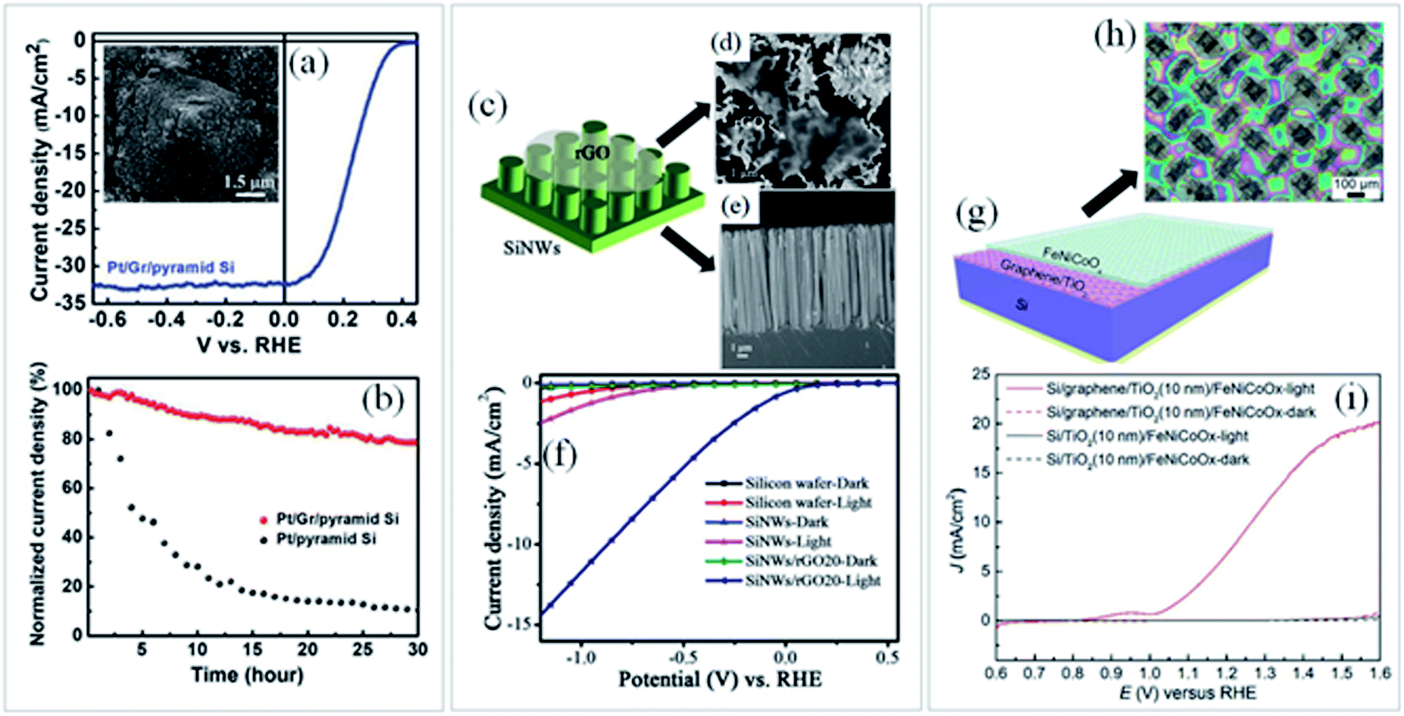 | ||
| Fig. 9 (a) Photocurrent density–potential curves of Pt/Gr/pyramid Si photocathode measured in 1 M HClO4 electrolyte under simulated illumination (AM 1.5G). The inset shows the SEM image of Pt NPs depositing on the surface of graphene/pyramid Si photocathode. (b) The stability test of the Pt/pristine pyramid Si and Pt/graphene/pyramid Si Schottky junction photocathode under illumination at a voltage of −0.3 VRHE. Reprinted with permission from ref. 41 Copyright 2019, Wiley-VCH. (c) Schematic illustration, (d) cross-section and (e) top view FESEM images for SiNWs/rGO20 composite. (f) Photocurrent density–potential curves of polished silicon wafer, SiNWs and SiNWs/rGO20 photocathodes measured in 0.1 M H2SO4 and 0.5 M K2SO4 electrolyte in the dark and under simulated illumination (AM 1.5G). Reprinted with permission from ref. 229 Copyright 2016, Royal Society of Chemistry. (g) Schematic structure and (h) optical image of the Si/Gr/TiO2/FeNiCoOx structure. (i) Photocurrent density–potential curves of Si/TiO2/FeNiCoOx and Si/graphene/TiO2/FeNiCoOx photoanodes measured in 1 M NaOH electrolyte in the dark and under simulated illumination (AM 1.5G). Reprinted with permission from ref. 230 Copyright 2018, Royal Society of Chemistry. | ||
Graphene and its derivatives could also be used as catalysts for a solar-driven hydrogen evolution reaction on Si-photocathodes. Fig. 9c–f displayed a schematic illustration, SEM images and PEC behaviour of Si nanowires (NWs) wafer covered with rGO and obtained by a facile and controllable electrochemical method.229 In these circumstances, rGO acts as an acceptor of the electrons generated in the Si NWs photocathode that improves the separation of the photogenerated charge carriers. Consequently, the enhancement of the photoelectrochemical performance of the SiNWs/rGO20 photocathode may be greatly attributed to the high electrical conductivity and the boosted charge transfer rate.
Generally, an integrated Si photoelectrode system for PEC water splitting requires a Si absorber, a protective layer and a catalytic layer.219 Fig. 9g and i, for example, illustrate the schematic structure, the optical image and PEC performance of the Si/graphene/TiO2/FeNiCoOx photoanode.230 The role of the rGO in the photoelectrode was attributed to the efficient charge separation at the interface (Si/graphene) and the defects in the graphene layer that provided electrochemically active sites for water oxidation. Other records also emphasize that the changes of the surface functional groups on graphene and its derivatives227 and the different graphene deposition techniques on the Si substrate224,226 can significantly influence the performance of PEC water splitting.
Fig. 10 displayed the best photocurrent performance of non-oxides photoelectrodes. Gr/Si-based photocathodes have the best photoresponse due to Si excellent properties as absorber where Gr or rGO is mainly used as protective layer in order to improve the photocathode stability during operation. However, techniques used to deposit the graphene layer are expensive which limits their scale-up. On the other hand, a complex system formed by a combination of TMCs and rGO has shown a promising and stable performance during operation as photocathode, but the use of Pt compromises its deployment. In addition, although graphene can catalyze the HER, the results are not satisfactory yet and new strategies need to be developed in the photocathodes design.
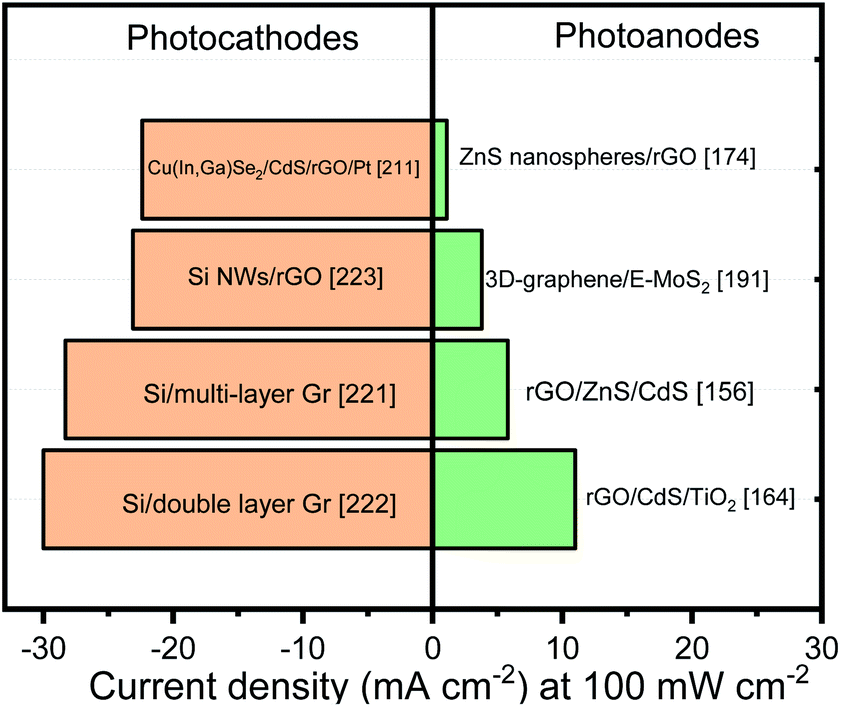 | ||
| Fig. 10 Photocurrent benchmark of graphene/non-oxides photoelectrodes. Data were extracted from various reports in the literature. | ||
In contrast, rGO/sulfide photoanodes synthesized by solvothermal methodologies have shown good PEC response. For these systems, graphene (and its derivatives) is employed not only as an electron acceptor and transporter but also as growth support, allowing the formation of optimized structures. As it can be noticed, the systems that have raised the maximal current are graphene/heterojunction nanocomposites, indicating that graphene by itself does not resolve the photoelectrodes limitations.
In case on non-oxide photoelectrodes, the incorporation of graphene sheets in the semiconductor matrix increases the photocurrent density value, without changing the Eonset. Furthermore, some factors directly affect the final performance of these photoelectrodes, including synthesis methodology, graphene content in the composite, semiconductor morphology, interfacial interaction and contact area between graphene and semiconductor.42
4 Final remarks and perspectives
The introduction of graphene in semiconducting photoelectrodes aiming the production of hydrogen and oxygen has become a potential strategy to design the next generation of photocatalysts. In this review, we have summarized the most recent accomplishments where graphene structures were combined with different semiconductor electrodes (metal oxides and non-metal oxides) in PEC applications. In all cases discussed, the insertion of graphene or other graphene derivatives has always led to an improvement in the performance and/or stability of the electrode. Regardless the positive and synergic effects, the mechanisms that drive the charge carrier dynamics within the system and how they operate are not fully understood, bringing new opportunities to be explored in the field.In view of charge carrier dynamics, graphene and its derivatives addition led to a more efficient charge transport through their layers compared to the photoelectrodes where grain boundaries and other defects act as charge carrier traps are present. Although for a single layer graphene, both electron and hole transport are possible and efficient, most samples are not pure or single layer graphene. Graphene oxide, doped graphene, reduced graphene oxide and other derivatives tend to benefit of one carrier to another. And even applying sophisticated techniques, it is hard to separate the effect on the electron or hole dynamics.
Many reports have demonstrated that graphene can also passivate the surface states in oxides and non-oxides photoelectrodes leading a significant enhancement performance and stability. Here, passivation also comes from the possibility to modify graphene edges and basal planes. Nevertheless, even if graphene has shown remarkable performance as protective layer, some reports has shown that the deposition methodologies bring inherent problems to accomplish this role.
Among graphene derivatives, rGO is the most employed probably associated with its facile synthesis and low-cost precursors. As graphene, rGO can acts as a passivation layer, excels the photoexcited charge carrier separation and, consequently, reduce their recombination at specific points of the electrode. An interesting application on rGO widely reported for non-oxide photoelectrodes consist in using it as growth supporting to create ordered structures with improved properties.
Incorporating GQDs on metal oxide photoelectrodes represents a promising and not extensively studied field. In addition to the charge separation/transport and stability gains, the coupled system formed by the photoelectrodes and GQDs also showed a superior light absorption compared to the non-coupled electrode which can be related to a higher photocurrent value. However, the amount of GQDs needs to be carefully controlled since this excess block the active sites and inhibits the OER/HER at the surface. In fact, this is an issue commonly found for other carbonaceous materials when incorporated in the electrodes.
Despite some studies present promising results in the field, some issues are still elusive; several reports affirm that a Schottky junction is formed between the semiconductor and the graphene but, to our knowledge, the junction nature between the semiconductors and graphene is still under debate and not fully understood. Otherwise, the usage of in situ/operando techniques to characterize graphene-bases photocatalysts is extremely valuable because they can provide fundamental aspects for sharpening our understanding on the nature of active sites, reaction mechanisms, and charge carrier dynamics. These techniques could also assist us to elucidate the chemical states and electronic structures, especially at the interface semiconductor–electrolyte.
Notwithstanding all the advantages presented in this review, it is important to point that better strategies to synthesize graphene coupled to photoelectrodes need to be developed. Despite all methodologies reported, the desired performance depends on a successful graphene addition or transfer to the substrate. For this reason, surface engineering plays an important role to further improve the PEC systems for water splitting.
The path ahead for graphene and its derivatives in photoelectrodes towards water splitting reactions is bright, but challenging, and many efforts in the chemistry and physics of these systems are still needed. The full understanding of how graphene operates may help us to tailor the properties of the semiconducting materials, to adjust the synergy and to gain benefits from all parts. We believe that for many years it will be a fascinating research area because of the many possibilities and opportunities.
Conflicts of interest
There are no conflicts to declare.Acknowledgements
The authors acknowledge CNPq/PCI/CTI (313069/2016-6) and FAPESP (2015/23775-3) for financial support. All authors fully acknowledge the support from the FAPESP (Grant 2017/11986-5) and Shell and the strategic importance of the support given by ANP (Brazil's National Oil, Natural Gas and Biofuels Agency) through the R&D Levy Regulation. A. F. N. also acknowledges the CNPq and INEO.Notes and references
- H. Cachet and E. M. M. Sutter, J. Phys. Chem. C, 2015, 119, 25548–25558 CrossRef CAS.
- S. Corby, E. Pastor, Y. Dong, X. Zheng, L. Francàs, M. Sachs, S. Selim, A. Kafizas, A. A. Bakulin and J. R. Durrant, J. Phys. Chem. Lett., 2019, 10, 5395–5401 CrossRef CAS PubMed.
- S. B. A. Hamid, S. J. Teh and C. W. Lai, Catalysts, 2017, 7, 93 CrossRef.
- I. Rodríguez-Gutiérrez, E. Djatoubai, J. Su, A. Vega-Poot, G. Rodríguez-Gattorno, F. L. Souza and G. Oskam, Sol. Energy Mater. Sol. Cells, 2020, 208, 110378 CrossRef.
- K. Sivula, F. Le Formal and M. Grätzel, ChemSusChem, 2011, 4, 432–449 CrossRef CAS PubMed.
- X. Wang, G. Chen, C. Zhou, Y. Yu and G. Wang, Eur. J. Inorg. Chem., 2012, 1742–1749 CrossRef CAS.
- Z. A. Lan, G. Zhang and X. Wang, Appl. Catal., B, 2016, 192, 116–125 CrossRef CAS.
- S. F. Duan, C. L. Tao, Y. Y. Geng, X. Q. Yao, X. W. Kang, J. Z. Su, I. Rodríguez-Gutiérrez, M. Kan, M. Romero, Y. Sun, Y. X. Zhao, D. D. Qin and Y. Yan, ChemCatChem, 2019, 11, 729–736 CrossRef CAS.
- Y. Fu, C. L. Dong, W. Zhou, Y. R. Lu, Y. C. Huang, Y. Liu, P. Guo, L. Zhao, W. C. Chou and S. Shen, Appl. Catal., B, 2020, 260, 118206 CrossRef CAS.
- P. S. Archana, N. Pachauri, Z. Shan, S. Pan and A. Gupta, J. Phys. Chem. C, 2015, 119, 15506–15516 CrossRef CAS.
- C. Zhai, M. Zhu, Y. Lu, F. Ren, C. Wang, Y. Du and P. Yang, Phys. Chem. Chem. Phys., 2014, 16, 14800–14807 RSC.
- A. K. Shah, T. K. Sahu, A. Banik, D. Gogoi, N. R. Peela and M. Qureshi, Sustainable Energy Fuels, 2019, 3, 1554–1561 RSC.
- X. An and J. C. Yu, RSC Adv., 2011, 1, 1426–1434 RSC.
- K. S. Novoselov, A. K. Geim, S. V. Morozov, D. Jiang, Y. Zhang, S. V. Dubonos, I. V. Grigorieva and A. A. Firsov, Science, 2004, 306, 666–669 CrossRef CAS PubMed.
- W. Xiong, F. Huang and R. Q. Zhang, Sustainable Energy Fuels, 2020, 4, 485–503 RSC.
- M. Yan, Y. Hua, F. Zhu, L. Sun, W. Gu and W. Shi, Appl. Catal., B, 2017, 206, 531–537 CrossRef CAS.
- C. Song, M. Fan, W. Shi and W. Wang, Environ. Sci. Pollut. Res., 2018, 25, 14486–14498 CrossRef CAS PubMed.
- G. S. Shanker, R. Bhosale, S. Ogale and A. Nag, Adv. Mater. Interfaces, 2018, 5, 1801488 CrossRef.
- G. Peng, M. Volokh, J. Tzadikov, J. Sun and M. Shalom, Adv. Energy Mater., 2018, 8, 1800566 CrossRef.
- S. J. Mun and S. J. Park, Catalysts, 2019, 9, 805 CrossRef CAS.
- W. Kong, X. Zhang, B. Chang, Y. Zhou, S. Zhang, G. He, B. Yang and J. Li, Electrochim. Acta, 2018, 282, 767–774 CrossRef CAS.
- J. Jing, M. Sun, Z. Chen, J. Li, F. Xu and L. Xu, J. Electrochem. Soc., 2017, 164, C822–C830 CrossRef CAS.
- S. Gong, Z. Jiang, S. Zhu, J. Fan, Q. Xu and Y. Min, J. Nanopart. Res., 2018, 20, 310 CrossRef.
- H. Bae, H. Rho, J. W. Min, Y. T. Lee, S. H. Lee, K. Fujii, H. J. Lee and J. S. Ha, Appl. Surf. Sci., 2017, 422, 354–358 CrossRef CAS.
- G. Peng, J. Qin, M. Volokh, C. Liu and M. Shalom, J. Mater. Chem. A, 2019, 7, 11718–11723 RSC.
- D. Chen, H. Zhang, Y. Liu and J. Li, Energy Environ. Sci., 2013, 6, 1362–1387 RSC.
- A. Adán-Más and D. Wei, Nanomaterials, 2013, 3, 325–356 CrossRef PubMed.
- Z. Zeng, S. Chen, T. T. Y. Tan and F. X. Xiao, Catal. Today, 2018, 315, 171–183 CrossRef CAS.
- C. Prasad, Q. Liu, H. Tang, G. Yuvaraja, J. Long, A. Rammohan and G. V. Zyryanov, J. Mol. Liq., 2020, 297, 111826 CrossRef CAS.
- Q. Huang, Z. Ye and X. Xiao, J. Mater. Chem. A, 2015, 3, 15824–15837 RSC.
- S. Wang, G. Liu and L. Wang, Chem. Rev., 2019, 119, 5192–5247 CrossRef CAS PubMed.
- M. G. Walter, E. L. Warren, J. R. Mckone, S. W. Boettcher, Q. Mi, E. A. Santori and N. S. Lewis, Chem. Rev., 2010, 110, 6446–6473 CrossRef CAS PubMed.
- M. Ni, M. K. H. Leung, D. Y. C. Leung and K. Sumathy, Renewable Sustainable Energy Rev., 2007, 11, 401–425 CrossRef CAS.
- M. R. Nellist, F. A. L. Laskowski, F. Lin, T. J. Mills and S. W. Boettcher, Acc. Chem. Res., 2016, 49, 733–740 CrossRef CAS PubMed.
- C. A. Koval and J. N. Howard, Chem. Rev., 1992, 92, 411–433 CrossRef CAS.
- M. G. Walter, E. L. Warren, J. R. Mckone, S. W. Boettcher, Q. Mi, E. A. Santori and N. S. Lewis, Chem. Rev., 2010, 110, 6446–6473 CrossRef CAS PubMed.
- P. Lianos, Appl. Catal., B, 2017, 210, 235–254 CrossRef CAS.
- Y. R. Kim, S. Bong, Y. J. Kang, Y. Yang, R. K. Mahajan, J. S. Kim and H. Kim, Biosens. Bioelectron., 2010, 25, 2366–2369 CrossRef CAS PubMed.
- C. Biswas and Y. H. Lee, Adv. Funct. Mater., 2011, 21, 3806–3826 CrossRef CAS.
- Y. Wang, Y. Wan and D. Zhang, Electrochem. Commun., 2010, 12, 187–190 CrossRef CAS.
- C. K. Ku, P. H. Wu, C. C. Chung, C. C. Chen, K. J. Tsai, H. M. Chen, Y. C. Chang, C. H. Chuang, C. Y. Wei, C. Y. Wen, T. Y. Lin, H. L. Chen, Y. S. Wang, Z. Y. Lee, J. R. Chang, C. W. Luo, D. Y. Wang, B. J. Hwang and C. W. Chen, Adv. Energy Mater., 2019, 9, 1901022 CrossRef.
- G. Xie, K. Zhang, B. Guo, Q. Liu, L. Fang and J. R. Gong, Adv. Mater., 2013, 25, 3820–3839 CrossRef CAS PubMed.
- D. Deng, K. S. Novoselov, Q. Fu, N. Zheng, Z. Tian and X. Bao, Nat. Nanotechnol., 2016, 11, 218–230 CrossRef CAS PubMed.
- S. Min and G. Lu, J. Phys. Chem. C, 2012, 116, 25415–25424 CrossRef CAS.
- C. X. Guo, H. Bin Yang, Z. M. Sheng, Z. S. Lu, Q. L. Song and C. M. Li, Angew. Chem., Int. Ed., 2010, 49, 3014–3017 CrossRef CAS.
- Y. T. Liang, B. K. Vijayan, K. A. Gray and M. C. Hersam, Nano Lett., 2011, 11, 2865–2870 CrossRef CAS PubMed.
- J. Guo, Y. Li, S. Zhu, Z. Chen, Q. Liu, D. Zhang, W. J. Moon and D. M. Song, RSC Adv., 2012, 2, 1356–1363 RSC.
- V. Georgakilas, M. Otyepka, A. B. Bourlinos, V. Chandra, N. Kim, K. C. Kemp, P. Hobza, R. Zboril and K. S. Kim, Chem. Rev., 2012, 112, 6156–6214 CrossRef CAS PubMed.
- C. Han, N. Zhang and Y. J. Xu, Nano Today, 2016, 11, 351–372 CrossRef CAS.
- D. R. Dreyer, A. D. Todd and C. W. Bielawski, Chem. Soc. Rev., 2014, 43, 5288–5301 RSC.
- B. Luo, S. Liu and L. Zhi, Small, 2012, 8, 630–646 CrossRef CAS PubMed.
- M. Cai, D. Thorpe, D. H. Adamson and H. C. Schniepp, J. Mater. Chem., 2012, 22, 24992–25002 RSC.
- S. P. Lonkar, Y. S. Deshmukh and A. A. Abdala, Nano Res., 2015, 8, 1039–1074 CrossRef CAS.
- C. Li and G. Shi, Adv. Mater., 2014, 26, 3992–4012 CrossRef CAS PubMed.
- T. F. Yeh, J. M. Syu, C. Cheng, T. H. Chang and H. Teng, Adv. Funct. Mater., 2010, 20, 2255–2262 CrossRef CAS.
- B. A. Aragaw, J. Nanostruct. Chem., 2020, 10, 9–18 CrossRef CAS.
- Z. Xu, M. Yin, J. Sun, G. Ding, L. Lu, P. Chang, X. Chen and D. Li, Nanotechnology, 2016, 27, 115401 CrossRef PubMed.
- Y. Yan, J. Chen, N. Li, J. Tian, K. Li, J. Jiang, J. Liu, Q. Tian and P. Chen, ACS Nano, 2018, 12, 3523–3532 CrossRef CAS PubMed.
- X. Cao, C. Xu, J. Ma, Y. Dong, C. Dong, M. Yue and Y. Ding, ChemSusChem, 2019, 12, 4685–4692 CrossRef CAS PubMed.
- F. Schedin, A. K. Geim, S. V. Morozov, E. W. Hill, P. Blake, M. I. Katsnelson and K. S. Novoselov, Nat. Mater., 2007, 6, 652–655 CrossRef CAS.
- C. Berger, Z. Song, T. Li, X. Li, A. Y. Ogbazghi, R. Feng, Z. Dai, N. Alexei, M. E. H. Conrad, P. N. First and W. A. De Heer, J. Phys. Chem. B, 2004, 108, 19912–19916 CrossRef CAS.
- A. C. Nielander, M. J. Bierman, N. Petrone, N. C. Strandwitz, S. Ardo, F. Yang, J. Hone and N. S. Lewis, J. Am. Chem. Soc., 2013, 135, 17246–17249 CrossRef CAS PubMed.
- S. Chen, L. Brown, M. Levendorf, W. Cai, S. Y. Ju, J. Edgeworth, X. Li, C. W. Magnuson, A. Velamakanni, R. D. Piner, J. Kang, J. Park and R. S. Ruoff, ACS Nano, 2011, 5, 1321–1327 CrossRef CAS.
- Y. Yang, S. Niu, D. Han, T. Liu, G. Wang and Y. Li, Adv. Energy Mater., 2017, 7, 1700555 CrossRef.
- I. Concina, Z. H. Ibupoto and A. Vomiero, Adv. Energy Mater., 2017, 7, 1700706 CrossRef.
- A. R. Marlinda, N. Yusoff, S. Sagadevan and M. R. Johan, Int. J. Hydrogen Energy, 2020, 45, 11976–11994 CrossRef CAS.
- T. F. Yeh, C. Y. Teng, S. J. Chen and H. Teng, Adv. Mater., 2014, 26, 3297–3303 CrossRef CAS.
- F. Behzadi, E. Saievar-Iranizad and A. Bayat, Mater. Res. Express, 2019, 6, 105615 CrossRef CAS.
- V. Mazánek, J. Luxa, S. Matějková, J. Kučera, D. Sedmidubský, M. Pumera and Z. Sofer, ACS Nano, 2019, 13, 1574–1582 Search PubMed.
- S. Amaral Carminati, A. do Nascimento Barbosa, A. Luiz Martins de Freitas, F. L. Freire, F. L. Souza and A. F. Nogueira, J. Catal., 2019, 372, 109–118 CrossRef CAS.
- J. Albero, D. Mateo and H. García, Molecules, 2019, 24, 906 CrossRef PubMed.
- J. Pu, L. Tang, C. Li, T. Li, L. Ling, K. Zhang, Q. Li and Y. Yao, RSC Adv., 2015, 5, 44142–44148 RSC.
- P. Y. Tang and J. Arbiol, Nanoscale Horiz., 2019, 4, 1256–1276 RSC.
- M. P. Cardona, M. Li, W. Li, J. McCall, D. Wang, Y. Li and C. Yang, Mater. Today Energy, 2018, 8, 8–14 CrossRef.
- R. Suresh, R. Udayabhaskar, C. Sandoval, E. Ramírez, R. V. Mangalaraja, H. D. Mansilla, D. Contreras and J. Yáñez, New J. Chem., 2018, 42, 8485–8493 RSC.
- L. Sang, L. Lei and C. Burda, Nano-Micro Lett., 2019, 11, 97 CrossRef CAS PubMed.
- J. Prakash, U. Prasad, R. Alexander, J. Bahadur, K. Dasgupta and A. N. M. Kannan, Langmuir, 2019, 35, 14492–14504 CrossRef CAS PubMed.
- S. Do Amaral Carminati, F. L. Souza and A. F. Nogueira, ChemPhysChem, 2016, 17, 170–177 CrossRef CAS PubMed.
- L. Sun, J. Sun, X. Yang, S. Bai, Y. Feng, R. Luo, D. Li and A. Chen, Dalton Trans., 2019, 48, 16091–16098 RSC.
- P. Subramanyam, T. Vinodkumar, D. Nepak, M. Deepa and C. Subrahmanyam, Catal. Today, 2019, 325, 73–80 CrossRef CAS.
- Y. S. Yun, G. Yoon, M. Park, S. Y. Cho, H.-D. Lim, H. Kim, Y. W. Park, B. H. Kim, K. Kang and H.-J. Jin, NPG Asia Mater., 2016, 8, e338 CrossRef.
- M. Cheng, R. Yang, L. Zhang, Z. Shi, W. Yang, D. Wang, G. Xie, D. Shi and G. Zhang, Carbon, 2012, 50, 2581–2587 CrossRef CAS.
- M. F. Craciun, S. Russo, M. Yamamoto and S. Tarucha, Nano Today, 2011, 6, 42–60 CrossRef CAS.
- J. Gliniak, J. H. Lin, Y. T. Chen, C. R. Li, E. Jokar, C. H. Chang, C. S. Peng, J. N. Lin, W. H. Lien, H. M. Tsai and T. K. Wu, ChemSusChem, 2017, 10, 3260–3267 CrossRef CAS PubMed.
- A. Bayat and E. Saievar-Iranizad, J. Alloys Compd., 2018, 755, 192–198 CrossRef CAS.
- M. H. Elbakkay, W. M. A. El Rouby, S. I. El-Dek and A. A. Farghali, Appl. Surf. Sci., 2018, 439, 1088–1102 CrossRef CAS.
- Q. Pan, K. Yang, G. Wang, D. Li, J. Sun, B. Yang, Z. Zou, W. Hu, K. Wen and H. Yang, Chem. Eng. J., 2019, 372, 399–407 CrossRef CAS.
- R. Azimirad, S. Safa, M. Ebrahimi, S. Yousefzadeh and A. Z. Moshfegh, J. Alloys Compd., 2017, 721, 36–44 CrossRef CAS.
- Z. Zhang, C. Gao, Y. Li, W. Han, W. Fu, Y. He and E. Xie, Nano Energy, 2016, 30, 892–899 CrossRef CAS.
- K. C. Bedin, D. N. F. Muche, M. A. Melo, A. L. M. Freitas, R. V. Gonçalves and F. L. Souza, ChemCatChem, 2020, 12, 3156–3169 CrossRef CAS.
- P. Tian, L. Tang, K. S. Teng and S. P. Lau, Mater. Today Chem., 2018, 10, 221–258 CrossRef CAS.
- X. Zhang, R. Wang, F. Li, Z. An, M. Pu and X. Xiang, Ind. Eng. Chem. Res., 2017, 56, 10711–10719 CrossRef CAS.
- T. Soltani, A. Tayyebi and B. K. Lee, Appl. Surf. Sci., 2018, 448, 465–473 CrossRef CAS.
- T. Soltani, A. Tayyebi and B. K. Lee, Sol. Energy Mater. Sol. Cells, 2018, 185, 325–332 CrossRef CAS.
- X. Han, Y. Wei, J. Su and Y. Zhao, ACS Sustainable Chem. Eng., 2018, 6, 14695–14703 CrossRef CAS.
- S. Ye, C. Ding, R. Chen, F. Fan, P. Fu, H. Yin, X. Wang, Z. Wang, P. Du and C. Li, J. Am. Chem. Soc., 2018, 140, 3250–3256 CrossRef CAS PubMed.
- Y. Hou, M. Qiu, T. Zhang, J. Ma, S. Liu, X. Zhuang, C. Yuan and X. Feng, Adv. Mater., 2017, 29, 1604480 CrossRef PubMed.
- J. Xie, J. Chen and C. M. Li, Int. J. Hydrogen Energy, 2017, 42, 7158–7165 CrossRef CAS.
- A. Kormányos, E. Kecsenovity, A. Honarfar, T. Pullerits and C. Janáky, Adv. Funct. Mater., 2020, 30, 2002124 CrossRef PubMed.
- L. Yu, Y. Zhang, J. He, H. Zhu, X. Zhou, M. Li, Q. Yang and F. Xu, J. Alloys Compd., 2018, 753, 601–606 CrossRef CAS.
- N. Ahmed, A. A. Farghali, W. M. A. El Rouby and N. K. Allam, Int. J. Hydrogen Energy, 2017, 42, 29131–29139 CrossRef CAS.
- Z. Zeng, T. Li, Y. B. Li, X. C. Dai, M. H. Huang, Y. He, G. Xiao and F. X. Xiao, J. Mater. Chem. A, 2018, 6, 24686–24692 RSC.
- H. S. Sajjadizadeh, E. K. Goharshadi and H. Ahmadzadeh, Int. J. Hydrogen Energy, 2020, 45, 123–134 CrossRef CAS.
- Z. Zeng, F. X. Xiao, X. Gui, R. Wang, B. Liu and T. T. Yang Tan, J. Mater. Chem. A, 2016, 4, 16383–16393 RSC.
- S. B. A. Hamid, S. J. Teh, C. W. Lai, S. Perathoner and G. Centi, J. Energy Chem., 2017, 26, 302–308 CrossRef.
- M. Ghorbani, H. Abdizadeh, M. Taheri and M. R. Golobostanfard, Int. J. Hydrogen Energy, 2018, 43, 7754–7763 CrossRef CAS.
- L. Sun, Y. Wang, F. Raziq, Y. Qu, L. Bai and L. Jing, Sci. Rep., 2017, 7, 1303 CrossRef PubMed.
- M. G. Hosseini, P. Y. Sefidi, Z. Aydin and S. Kinayyigit, Electrochim. Acta, 2020, 333, 135475 CrossRef CAS.
- Z. Zhao, L. Zheng, W. Hu and H. Zheng, Electrochim. Acta, 2018, 292, 322–330 CrossRef CAS.
- J. Ke, H. Zhou, J. Liu, Z. Zhang, X. Duan and S. Wang, J. Colloid Interface Sci., 2019, 555, 413–422 CrossRef CAS PubMed.
- I. V. Bagal, N. R. Chodankar, M. A. Hassan, A. Waseem, M. A. Johar, D. H. Kim and S. W. Ryu, Int. J. Hydrogen Energy, 2019, 44, 21351–21378 CrossRef CAS.
- A. Kushwaha, R. S. Moakhar, G. K. L. Goh and G. K. Dalapati, J. Photochem. Photobiol., A, 2017, 337, 54–61 CrossRef CAS.
- D. Chen, Z. Liu, Z. Guo, W. Yan and M. Ruan, Chem. Eng. J., 2020, 381, 122655 CrossRef CAS.
- M. I. Díez-García, T. Lana-Villarreal and R. Gómez, ChemSusChem, 2016, 9, 1504–1512 CrossRef PubMed.
- G. P. Wheeler and K. S. Choi, ACS Appl. Energy Mater., 2018, 1, 4917–4923 CrossRef CAS.
- A. A. Dubale, W. N. Su, A. G. Tamirat, C. J. Pan, B. A. Aragaw, H. M. Chen, C. H. Chen and B. J. Hwang, J. Mater. Chem. A, 2014, 2, 18383–18397 RSC.
- M. M. Momeni and Y. Ghayeb, J. Alloys Compd., 2015, 637, 393–400 CrossRef CAS.
- Y. Ghayeb, M. M. Momeni and M. Menati, J. Mater. Sci.: Mater. Electron., 2017, 28, 7650–7659 CrossRef CAS.
- C. Das, B. Ananthoju, A. K. Dhara, M. Aslam, S. K. Sarkar and K. R. Balasubramaniam, Adv. Mater. Interfaces, 2017, 4, 1–10 Search PubMed.
- C. Ma, D. K. Ma, W. Yu, W. Chen and S. Huang, Appl. Surf. Sci., 2019, 481, 661–668 CrossRef CAS.
- C. Ma, D. K. Ma, W. Yu, W. Chen and S. Huang, Appl. Surf. Sci., 2019, 481, 661–668 CrossRef CAS.
- H. V. Le, L. T. Le, P. D. Tran, J. S. Chang, U. T. Dieu Thuy and N. Q. Liem, Int. J. Hydrogen Energy, 2019, 44, 14635–14641 CrossRef CAS.
- C. Yu and X. Zhang, ChemElectroChem, 2019, 6, 2004–2012 CrossRef CAS.
- J. Su, L. Guo, N. Bao and C. A. Grimes, Nano Lett., 2011, 11, 1928–1933 CrossRef CAS PubMed.
- X. Li, R. Shen, S. Ma, X. Chen and J. Xie, Appl. Surf. Sci., 2018, 430, 53–107 CrossRef CAS.
- M. Reza Gholipour, C. T. Dinh, F. Béland and T. O. Do, Nanoscale, 2015, 7, 8187–8208 RSC.
- M. A. Melo, Z. Wu, B. A. Nail, A. T. De Denko, A. F. Nogueira and F. E. Osterloh, Nano Lett., 2018, 18, 805–810 CrossRef CAS PubMed.
- T. T. A. Lucas, M. A. Melo, A. L. M. Freitas, F. L. Souza and R. V. Gonçalves, Sol. Energy Mater. Sol. Cells, 2020, 208, 110428 CrossRef CAS.
- B. M. Almeida, M. A. Melo, J. Bettini, J. E. Benedetti and A. F. Nogueira, Appl. Surf. Sci., 2015, 324, 419–431 CrossRef CAS.
- S. J. A. Moniz, S. A. Shevlin, D. J. Martin, Z. X. Guo and J. Tang, Energy Environ. Sci., 2015, 8, 731–759 RSC.
- A. Iwase, S. Yoshino, T. Takayama, Y. H. Ng, R. Amal and A. Kudo, J. Am. Chem. Soc., 2016, 138, 10260–10264 CrossRef CAS PubMed.
- Y. Hou, F. Zuo, A. Dagg and P. Feng, Nano Lett., 2012, 12, 6464–6473 CrossRef CAS PubMed.
- A. Iwase, Y. H. Ng, Y. Ishiguro, A. Kudo and R. Amal, J. Am. Chem. Soc., 2011, 133, 11054–11057 CrossRef CAS PubMed.
- Z. Pan, G. Zhang and X. Wang, Angew. Chem., Int. Ed., 2019, 58, 7102–7106 CrossRef CAS PubMed.
- M. A. Melo and F. E. Osterloh, ACS Appl. Mater. Interfaces, 2018, 10, 27195–27204 CrossRef CAS PubMed.
- H. M. El-Bery, Y. Matsushita and A. Abdel-moneim, Appl. Surf. Sci., 2017, 423, 185–196 CrossRef CAS.
- T. F. Hou, A. Shanmugasundaram, M. A. Hassan, M. A. Johar, S. W. Ryu and D. W. Lee, Int. J. Hydrogen Energy, 2019, 44, 19177–19192 CrossRef CAS.
- W. Fan, X. Yu, H. C. Lu, H. Bai, C. Zhang and W. Shi, Appl. Catal., B, 2016, 181, 7–15 CrossRef CAS.
- B. Bazri, E. Kowsari, N. Seifvand and N. Naseri, J. Electroanal. Chem., 2019, 843, 1–11 CrossRef CAS.
- C. S. Yaw, J. Tang, A. K. Soh and M. N. Chong, Chem. Eng. J., 2020, 380, 122501 CrossRef CAS.
- Y. Yan, C. Wang, X. Yan, L. Xiao, J. He, W. Gu and W. Shi, J. Phys. Chem. C, 2014, 118, 23519–23526 CrossRef CAS.
- S. Bai, J. Han, Y. Zhao, H. Chu, S. Wei, J. Sun, L. Sun, R. Luo, D. Li and A. Chen, Renewable Energy, 2020, 148, 380–387 CrossRef CAS.
- M. Wang, P. Ju, J. Li, Y. Zhao, X. Han and Z. Hao, ACS Sustain. Chem. Eng., 2017, 5, 7878–7886 CrossRef CAS.
- Q. Quan, S. Xie, B. Weng, Y. Wang and Y. J. Xu, Small, 2018, 14, 1–11 Search PubMed.
- E. Ha, W. Liu, L. Wang, H. W. Man, L. Hu, S. C. E. Tsang, C. T. L. Chan, W. M. Kwok, L. Y. S. Lee and K. Y. Wong, Sci. Rep., 2017, 7, 1–8 CrossRef PubMed.
- M. Seol, J. W. Jang, S. Cho, J. S. Lee and K. Yong, Chem. Mater., 2013, 25, 184–189 CrossRef CAS.
- M. Alves Melo Júnior, A. Morais and A. F. Nogueira, Microporous Mesoporous Mater., 2016, 234, 1–11 CrossRef.
- M. U. Azam, M. Tahir, M. Umer, B. Tahir, N. Shehzad and M. Siraj, Int. J. Hydrogen Energy, 2019, 44, 23669–23688 CrossRef CAS.
- S. Yousefzadeh, M. Faraji and A. Z. Moshfegh, J. Electroanal. Chem., 2016, 763, 1–9 CrossRef CAS.
- L. Pan, J. H. Kim, M. T. Mayer, M. K. Son, A. Ummadisingu, J. S. Lee, A. Hagfeldt, J. Luo and M. Grätzel, Nat. Catal., 2018, 1, 412–420 CrossRef CAS.
- H. Ahmad, S. K. Kamarudin, L. J. Minggu and M. Kassim, Renewable Sustainable Energy Rev., 2015, 43, 599–610 CrossRef CAS.
- S. L. Lee and C. J. Chang, Catalysts, 2019, 9, 457 CrossRef CAS.
- Y. Zhu, J. Chen, L. Shao, X. Xia, Y. Liu and L. Wang, Appl. Catal., B, 2020, 268, 118744 CrossRef CAS.
- S. Sharma, D. Kumar and N. Khare, Int. J. Hydrogen Energy, 2019, 44, 3538–3552 CrossRef CAS.
- S. Tonda, S. Kumar, Y. Gawli, M. Bhardwaj and S. Ogale, Int. J. Hydrogen Energy, 2017, 42, 5971–5984 CrossRef CAS.
- W. Zhang, S. Huo, S. Yang, Y. Zhong, S. Zhang, H. Wang, X. Zhong and Y. Fang, Chem.–Asian J., 2019, 14, 3431–3441 CrossRef CAS PubMed.
- R. Bin Wei, P. Y. Kuang, H. Cheng, Y. B. Chen, J. Y. Long, M. Y. Zhang and Z. Q. Liu, ACS Sustainable Chem. Eng., 2017, 5, 4249–4257 CrossRef.
- J. Xue, L. Long, L. Zhang, H. Luo, L. Yang, F. Liu, F. Lv, W. Kong and J. Liu, Int. J. Hydrogen Energy, 2020, 45, 6476–6486 CrossRef CAS.
- N. Zhang, S. H. Li, X. Fu and Y. J. Xu, Pure Appl. Chem., 2018, 90, 1379–1392 CrossRef CAS.
- M. Faraji, M. Yousefi, S. Yousefzadeh, M. Zirak, N. Naseri, T. H. Jeon, W. Choi and A. Z. Moshfegh, Energy Environ. Sci., 2019, 12, 59–95 RSC.
- M. Shaban, M. Rabia, A. M. A. El-Sayed, A. Ahmed and S. Sayed, Sci. Rep., 2017, 7, 14100 CrossRef PubMed.
- H. S. Lin and L. Y. Lin, Electrochim. Acta, 2017, 252, 235–244 CrossRef CAS.
- D. Akyüz, R. M. Zunain Ayaz, S. Yılmaz, Ö. Uğuz, C. Sarıoğlu, F. Karaca, A. R. Özkaya and A. Koca, Int. J. Hydrogen Energy, 2019, 44, 18836–18847 CrossRef.
- D. Zhao and C. F. Yang, Renewable Sustainable Energy Rev., 2016, 54, 1048–1059 CrossRef CAS.
- L. Cai, Y. Du, X. Guan and S. Shen, Chin. Chem. Lett., 2019, 30, 2363–2367 CrossRef CAS.
- Y. Rambabu, S. Dhua, M. Jaiswal and S. C. Roy, Nanotechnology, 2020, 31, 275701 CrossRef CAS PubMed.
- L. Li, J. Wu, B. Liu, X. Liu, C. Li, Y. Gong, Y. Huang and L. Pan, Catal. Today, 2018, 315, 110–116 CrossRef CAS.
- C. Xue, X. Yan, H. An, H. Li, J. Wei and G. Yang, Appl. Catal., B, 2018, 222, 157–166 CrossRef CAS.
- X. Wang, J. Xie and C. M. Li, J. Mater. Chem. A, 2015, 3, 1235–1242 RSC.
- S. Alhammadi, V. R. M. Reddy, S. Gedi, H. Park, M. S. Sayed, J. J. Shim and W. K. Kim, Nanomaterials, 2020, 10, 245 CrossRef CAS PubMed.
- W. Han, L. Chen, W. Song, S. Wang, X. Fan, Y. Li, F. Zhang, G. Zhang and W. Peng, Appl. Catal., B, 2018, 236, 212–221 CrossRef CAS.
- X. Zhang, W. An, Y. Li, J. Hu, H. Gao and W. Cui, Int. J. Hydrogen Energy, 2018, 43, 9902–9913 CrossRef CAS.
- M. Zubair, I. H. Svenum, M. Rønning and J. Yang, Catalysts, 2020, 10, 358 CrossRef CAS.
- T. Mahvelati-Shamsabadi and E. K. Goharshadi, Sol. Energy, 2018, 161, 226–234 CrossRef CAS.
- M. Azarang, M. Sookhakian, M. Aliahmad, M. Dorraj, W. J. Basirun, B. T. Goh and Y. Alias, Int. J. Hydrogen Energy, 2018, 43, 14905–14914 CrossRef CAS.
- C. J. Chang, Y. H. Wei and K. P. Huang, Int. J. Hydrogen Energy, 2017, 42, 23578–23586 CrossRef CAS.
- C. J. Chang, Y. G. Lin, H. T. Weng and Y. H. Wei, Appl. Surf. Sci., 2018, 451, 198–206 CrossRef CAS.
- J. Li, X. Zhang, L. Song, M. Zhang and B. Zhang, J. Energy Chem., 2016, 25, 654–658 CrossRef.
- A. Morais, S. do Amaral Carminati and A. F. Nogueira, in Physical Chemistry of Interfaces and Nanomaterials XV, 2016, vol. 9923, p. 992314 Search PubMed.
- Y. Hu, X. Ren, H. Qiao, Z. Huang, X. Qi and J. Zhong, Sol. Energy, 2017, 157, 905–910 CrossRef CAS.
- S. Pulipaka, A. K. S. Koushik, N. Boni, M. Deepa and P. Meduri, Int. J. Hydrogen Energy, 2019, 44, 11584–11592 CrossRef CAS.
- Y. J. Yuan, H. W. Lu, Z. T. Yu and Z. G. Zou, ChemSusChem, 2015, 8, 4113–4127 CrossRef CAS PubMed.
- S. Kumar, N. L. Reddy, H. S. Kushwaha, A. Kumar, M. V. Shankar, K. Bhattacharyya, A. Halder and V. Krishnan, ChemSusChem, 2017, 10, 3588–3603 CrossRef CAS PubMed.
- H. Qiao, Z. Huang, S. Liu, Y. Tao, H. Zhou, M. Li and X. Qi, J. Phys. Chem. C, 2019, 123, 10949–10955 CrossRef CAS.
- C. K. Sumesh and S. C. Peter, Dalton Trans., 2019, 48, 12772–12802 RSC.
- M. Ben Ali, W. K. Jo, H. Elhouichet and R. Boukherroub, Int. J. Hydrogen Energy, 2017, 42, 16449–16458 CrossRef CAS.
- H. Mu, J. Wan, Y. Wu, J. Xu, L. Wang and X. Cao, Int. J. Hydrogen Energy, 2018, 43, 18105–18114 CrossRef CAS.
- S. Chakrabarty, A. Mukherjee and S. Basu, ACS Sustainable Chem. Eng., 2018, 6, 5238–5247 CrossRef CAS.
- T. Huang, Y. Luo, W. Chen, J. Yao and X. Liu, ACS Sustainable Chem. Eng., 2018, 6, 4671–4679 CrossRef CAS.
- T. Huang, Y. Hua, J. Yao, Y. Luo and X. Liu, Mater. Chem. Phys., 2018, 212, 506–512 CrossRef CAS.
- X. Li, S. Guo, W. Li, X. Ren, J. Su, Q. Song, A. J. Sobrido and B. Wei, Nano Energy, 2019, 57, 388–397 CrossRef CAS.
- M. Huang, Y. Zhou, Y. Guo, H. Wang, X. Hu, X. Xu and Z. Ren, J. Mater. Sci., 2018, 53, 7744–7754 CrossRef CAS.
- M. Wang, X. Han, Y. Zhao, J. Li, P. Ju and Z. Hao, J. Mater. Sci., 2018, 53, 3603–3612 CAS.
- Y. J. Yuan, Y. Yang, Z. Li, D. Chen, S. Wu, G. Fang, W. Bai, M. Ding, L. X. Yang, D. P. Cao, Z. T. Yu and Z. G. Zou, ACS Appl. Energy Mater., 2018, 1, 1400–1407 CrossRef CAS.
- O. Y. Posudievsky, O. A. Kozarenko, V. S. Dyadyun, V. G. Koshechko and V. D. Pokhodenko, Electrocatalysis, 2019, 10, 477–488 CrossRef CAS.
- R. Carrizo, D. Ramírez, L. Hernández, G. Lobos, P. Häberle, E. A. Dalchiele and G. Riveros, ChemElectroChem, 2019, 6, 1047–1056 CrossRef CAS.
- P. D. Matthews, P. D. McNaughter, D. J. Lewis and P. O'Brien, Chem. Sci., 2017, 8, 4177–4187 RSC.
- S. Kai, B. Xi, D. Wei and S. Xiong, Nanoscale, 2019, 11, 5571–5579 RSC.
- W. Bo, Z. Liu, T. Hong, J. Han, K. Guo, X. Zhang and D. Chen, J. Nanopart. Res., 2015, 17, 295 CrossRef.
- J. Nong, G. Lan, W. Jin, P. Luo, C. Guo, X. Tang, Z. Zang and W. Wei, J. Mater. Chem. C, 2019, 7, 9830–9839 RSC.
- S. Manchala, V. S. R. K. Tandava, L. R. Nagappagari, S. Muthukonda Venkatakrishnan, D. Jampaiah, Y. M. Sabri, S. K. Bhargava and V. Shanker, Photochem. Photobiol. Sci., 2019, 18, 2952–2964 CrossRef CAS PubMed.
- F. Xing, Q. Liu and C. Huang, Sol. RRL, 2020, 4, 1900483 CrossRef CAS.
- C. Du, B. Yan, Z. Lin and G. Yang, Catal. Sci. Technol., 2019, 9, 4066–4076 RSC.
- Y. Xia, Q. Li, K. Lv, D. Tang and M. Li, Appl. Catal., B, 2017, 206, 344–352 CrossRef CAS.
- R. Bao, J. Geng, J. A. Sullivan, J. Xia, W. Wang, W. Y. Wong and H. Li, Phys. Status Solidi A, 2018, 215, 1800436 CrossRef.
- X. Zou and Y. Zhang, Chem. Soc. Rev., 2015, 44, 5148–5180 RSC.
- I. A. Rusetskyi, M. O. Danilov, S. S. Fomanyuk, I. A. Slobodyanyuk, V. S. Vorobets and G. Y. Kolbasov, Res. Chem. Intermed., 2019, 45, 4121–4132 CrossRef CAS.
- G. Zhu, X. Xie, X. Li, Y. Liu, X. Shen, K. Xu and S. Chen, ACS Appl. Mater. Interfaces, 2018, 10, 19258–19270 CrossRef CAS PubMed.
- L. Jiang, J. Chen, Y. Wang, K. Sun, F. Liu and Y. Lai, Mater. Lett., 2018, 224, 109–112 CrossRef CAS.
- L. Jia, X. Sun, Y. Jiang, S. Yu and C. Wang, Adv. Funct. Mater., 2015, 25, 1814–1820 CrossRef CAS.
- B. Koo, S. Byun, S. W. Nam, S. Y. Moon, S. Kim, J. Y. Park, B. T. Ahn and B. Shin, Adv. Funct. Mater., 2018, 28, 1705136 CrossRef.
- P. Kumar, R. Boukherroub and K. Shankar, J. Mater. Chem. A, 2018, 6, 12876–12931 RSC.
- J. Li, Z. Zhao, Y. Ma and Y. Qu, ChemCatChem, 2017, 9, 1554–1568 CrossRef CAS.
- C. Xue, H. An, X. Yan, J. Li, B. Yang, J. Wei and G. Yang, Nano Energy, 2017, 39, 513–523 CrossRef CAS.
- Q. Chen, Z. Wang, K. Chen, Q. Fu, Y. Liu, Y. Zhang, D. Li and C. Pan, RSC Adv., 2019, 9, 33747–33754 RSC.
- K. A. Tsai and Y. J. Hsu, Appl. Catal., B, 2015, 164, 271–278 CrossRef CAS.
- H. Qiao, Z. Huang, X. Ren, H. Yao, S. Luo, P. Tang, X. Qi and J. Zhong, J. Mater. Sci., 2018, 53, 4371–4377 CrossRef CAS.
- X. Li, L. Zhang, M. Huang, S. Wang, X. Li and H. Zhu, J. Mater. Chem. A, 2016, 4, 14789–14795 RSC.
- R. Fan, Z. Mi and M. Shen, Opt. Express, 2019, 27, A51 CrossRef CAS PubMed.
- S. Lee, S. Cha, Y. Myung, K. Park, I. H. Kwak, I. S. Kwon, J. Seo, S. A. Lim, E. H. Cha and J. Park, ACS Appl. Mater. Interfaces, 2018, 10, 33198–33204 CrossRef CAS PubMed.
- S. M. Thalluri, B. Wei, K. Welter, R. Thomas, V. Smirnov, L. Qiao, Z. Wang, F. Finger and L. Liu, ACS Energy Lett., 2019, 4, 1755–1762 CrossRef CAS.
- M. Kan, X. Qian, T. Zhang, D. Yue and Y. Zhao, ACS Sustainable Chem. Eng., 2017, 5, 10940–10946 CrossRef CAS.
- C. Li, Q. Cao, F. Wang, Y. Xiao, Y. Li, J. J. Delaunay and H. Zhu, Chem. Soc. Rev., 2018, 47, 4981–5037 RSC.
- C. P. Han, C. J. Chen, C. C. Hsu, A. Jena, H. Chang, N. C. Yeh, S. F. Hu and R. S. Liu, Catal. Today, 2019, 335, 395–401 CrossRef CAS.
- U. Sim, J. Moon, J. Lee, J. An, H. Y. Ahn, D. J. Kim, I. Jo, C. Jeon, S. Han, B. H. Hong and K. T. Nam, ACS Appl. Mater. Interfaces, 2017, 9, 3570–3580 CrossRef CAS PubMed.
- Y. Sim, J. John, J. Moon and U. Sim, Appl. Sci., 2018, 8, 2046 CrossRef CAS.
- K. Alam, Y. Sim, J. H. Yu, J. Gnanaprakasam, H. Choi, Y. Chae, U. Sim and H. Cho, Materials, 2020, 13, 12 CrossRef CAS PubMed.
- J. Nong, W. Wei, X. Song, L. Tang, J. Yang, T. Sun, L. Yu, W. Luo, C. Li and D. Wei, Surf. Coat. Technol., 2017, 320, 579–583 CrossRef CAS.
- H. Meng, K. Fan, J. Low and J. Yu, Dalton Trans., 2016, 45, 13717–13725 RSC.
- C. Li, Y. Xiao, L. Zhang, Y. Li, J. J. Delaunay and H. Zhu, Sustainable Energy Fuels, 2018, 2, 663–672 RSC.
Footnote |
| † These authors contributed equally to this work. |
| This journal is © The Royal Society of Chemistry 2021 |