
 Open Access Article
 This Open Access Article is licensed under a Creative Commons Attribution-Non Commercial 3.0 Unported Licence
Comparison of diamond nanoparticles captured on the floating and grounded membranes in the hot filament chemical vapor deposition process†
Hwan-Young Kima,
Da-Seul Kima and
Nong-Moon Hwang *ab
*ab
aDepartment of Materials Science and Engineering, Seoul National University, 1 Gwanak-ro, Gwanak-gu, Seoul, Republic of Korea. E-mail: welcome777@snu.ac.kr; nmhwang@snu.ac.kr
bResearch Institute of Advanced Materials, 599 Gwanak-ro, Gwanak-gu, Seoul, Republic of Korea
First published on 2nd February 2021
Abstract
Negatively charged diamond nanoparticles are known to be generated in the gas phase of the hot filament chemical vapor deposition (HFCVD) process. However, the structures of these nanoparticles remain unknown. Also, the effect of charging on the stability of nanodiamond structures has not been studied experimentally. Here, by installing a capturing apparatus in an HFCVD reactor, we succeeded in capturing nanoparticles on the floating and grounded SiO, carbon, and graphene membranes of a copper transmission electron microscope grid during HFCVD. We examined the effect of charge on the crystal structure of nanodiamonds captured for 10 s under various conditions and identified four carbon allotropes, which are i-carbon, hexagonal diamond, n-diamond, and cubic diamond, by analyzing 150 d-spacings of ∼100 nanoparticles for each membrane. Nanoparticles captured on the floating membrane consisted mainly of cubic diamond and n-diamond, whereas those captured on the grounded membrane consisted mainly of i-carbon. Diamond particles deposited for 8 h on the floating silicon (Si) substrate exhibited an octahedron shape with well-developed facets, and a high-intensity 1332 cm−1 Raman peak, whereas diamond particles deposited on the grounded Si substrate showed a spherical shape partially covered with crystalline facets with a broad G-band Raman peak. These results indicate that charging stabilizes the diamond structure.
1. Introduction
Since 1963, nanodiamonds have been synthesized by hydrothermal synthesis,1–3 microwave plasma chemical vapor deposition (CVD),4 ion bombardment,5 ball milling of high-pressure/high-temperature diamond,6 and detonation of carbon explosives.7 Nanodiamonds have been widely studied in the fields of medicine,8 biology,9 optoelectronics,10 and quantum computers.11 It took nearly 40 years to characterize and isolate dispersed nanoparticles of 4–5 nm.12,13 Hydrocarbon, CnHm, with hydrogen atoms terminating all dangling bonds of surface carbon atoms, is known to stabilize a surface structure of nanodiamonds.14 The presence of atomic hydrogen is a crucial factor in the low-pressure synthesis of diamond.15–17 However, recent studies showed that diamond can be synthesized without atomic hydrogen.18–20 High-purity diamond microparticles have been produced using electric pulse discharge in a low-pressure process.19 Yoshimoto et al.20 reported the nucleation and growth of diamond on a single-crystal sapphire substrate by laser ablation in a hydrogen-free, pure oxygen environment. In the synthesis of diamond without atomic hydrogen, the common processing parameter is the plasma, wherein charged species such as electrons and ions are generated. Lai and Barnard21 used density functional theory-based tight binding calculations to investigate the effect of charge on the surface stability of nanodiamonds. They reported that negative charges stabilized the surface of sp3-bonded carbon atoms and induced dehydrogenation from the surface of nanodiamond. Additionally, the negative charging saturates the dangling bonds of carbon atoms, resulting in the disappearance of reconstructed graphitized layers at the surface, whereas positive charging partially breaks the connection between the core and shell, forming a new layer of graphene-like carbons.22 However, it is difficult to confirm the effect of charge on the phase stability of nanodiamonds experimentally, which is why there have been no experimental studies on this to date.Hwang et al.23 suggested that charge plays an important role in the gas-phase nucleation of diamond, providing the site for ion-induced nucleation and as a result generating charged diamond nanoparticles in hot filament chemical vapor deposition (HFCVD). They suggested further that negatively charged diamond nanoparticles are the building blocks of diamond films. The generation of negatively charged carbon nanoparticles in the HFCVD process was confirmed experimentally using a Wien filter and an energy analyser.24,25
According to these reports, non-aggregated diamond nanoparticles can be synthesized using the HFCVD process. This method has many advantages. First, the size of nanoparticles can be controlled by adjusting the processing parameter. Second, isolated high quality single crystalline diamond nanoparticles can be synthesized. Third, doping of elements such as silicon and nitrogen is relatively easy, which is important for photoluminescence applications. In relation to this possibility for the synthesis of diamond nanoparticles using HFCVD, Park et al.26 recently showed that negatively charged diamond nanoparticles of 4–6 nm were generated during HFCVD, by capturing them on the membrane of a transmission electron microscope (TEM) grid.
If charged diamond nanoparticles are generated in the gas phase of the HFCVD process, their capturing behavior would depend on whether the capturing membrane is electrically floating or grounded. Additionally, the deposition behavior of diamond would also depend on whether the substrate is floating or grounded. The purpose of this study was to compare nanoparticles captured for 10 s on floating and grounded membranes, and to compare diamond deposited for 8 h on floating and grounded substrates in the HFCVD process.
2. Experimental procedure
Diamond nanoparticles were captured using the capturing system in an HFCVD reactor, which is schematically shown in Fig. 1. The filament consisted of three 0.5 mmø tungsten wires, which were twisted into a nine-turn coil of 8 mmø. The filament temperature and reactor pressure were 2000 °C and 20 torr, respectively. The gas mixture of 1% CH4–99% H2 or 3% CH4–97% H2 was supplied at 100 standard cubic centimeters per minute (sccm), using a mass flow controller. For reproducibility of the experiment, the tungsten filament was carburized for 24 h at 1% CH4–99% H2 or 3% CH4–97% H2 before nanoparticles were captured.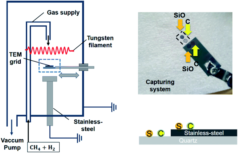 | ||
| Fig. 1 Schematics of the experimental apparatus for capturing carbon nanoparticles. The left figure is the HWCVD reactor with a capturing apparatus. The right figure illustrates how the SiO and carbon membranes are made electrically floating and grounded. Nanoparticles were captured on floating and grounded SiO and carbon membranes under the same HFCVD condition. ‘S’ and ‘C’ in the right figure indicate SiO and carbon membranes, respectively. | ||
Nanoparticles were captured on the carbon membrane (lacey carbon film; Ted Pella, Inc, Redding, CA, USA), SiO membrane (Ted Pella, Inc.), and graphene membrane (6–8 layers of graphene film; Ted Pella, Inc.) of a copper (Cu) TEM grid. The carbon and SiO membranes were subjected to scanning TEM (STEM) imaging by a Tecnai F20 TEM instrument (FEI, Hillsboro, OR, USA). The graphene membrane was used to obtain high-resolution TEM (HR-TEM) images using a JEM-2100F system (JEOL Ltd., Tokyo, Japan). The TEM grids were placed in a quartz holder or stainless steel holder connected to the capturing apparatus. The capturing apparatus could be positioned in the capture zone as needed and retracted back towards the chamber wall. The grid was exposed for a capturing time of 10 s. Due to thermal damage to the membranes at temperatures above ∼650 °C, the capture zone was located 30 mm below the hot filament. The temperature in the capture zone was ∼600 °C when using the 3% CH4–97% H2 gas mixture. Additionally, graphene membranes at a capture temperature of ∼600 °C with the 1% CH4–99% H2 gas mixture were stable and used to examine charging effects. Before pushing the capturing apparatus into the capture zone, the tungsten filament was additionally carburized for 30 min under the same conditions as those for diamond deposition.
Most of the captured nanoparticles were single crystals, which were chosen for phase identification. The lattice parameters and lattice angles were determined from the fast Fourier transform (FFT) image of each nanoparticle. The crystal structures of the captured nanoparticles were determined by reference to the information provided by the Joint Committee on Powder Diffraction Standards (JCPDS) on the reported carbon allotropes. To identify the crystal structure of the captured nanoparticles, we analyzed 150 d-spacing values of ∼100 nanoparticles on each membrane. Four carbon allotropes of i-carbon, hexagonal diamond, n-diamond, and cubic diamond were identified from the HFCVD process.
The deposition behavior of diamond was compared between electrically floating and grounded p-type 〈100〉 silicon (Si) substrates (size: 10 × 10 × 3 mm3). For grounding, the Si substrate was placed on the stainless-steel substrate holder connected to external ground. For floating, the Si substrate was placed on a 10 × 10 × 1 mm3 sapphire plate, which was again placed on the stainless-steel substrate holder. The diamond was deposited for 8 h onto the Si substrate at a substrate temperature of 950 °C, with the substrate placed 5 mm below the filament. The microstructure of the deposited diamond was observed by field-emission scanning electron microscopy (FE-SEM; SU70; Hitachi Ltd., Tokyo, Japan). The deposited diamond was analyzed using a Raman spectrometer (LabRam HR Evolution; Horiba Ltd., Kyoto, Japan) with a diode-pumped solid-state laser beam (exciting radiation wavelength: 532.3 nm; spot size: 1 μm).
3. Results and discussion
The nanoparticles in the gas phase are negatively charged. One possible route to negative charging27 is the negative surface ionization of carbon molecules of high electron affinity such as C2, which has an electron affinity of 3.54 eV.28 The negatively charged carbon molecules would act as a site for ion-induced nucleation and grow as charged nuclei. Another possible route to negative charging is neutral nucleation, followed by the attachment of electrons emitted from the hot filament. Several different types of membranes for the TEM grid are required to investigate the electrical properties of nanoparticles. The negatively charged nanoparticles would have a Coulomb-repulsion interaction with the negatively charged surface of the substrate.26 Fig. 2a and b show STEM images of nanoparticles on SiO; Fig. 2c and d show STEM images of nanoparticles on the carbon membranes. In the setup shown in Fig. 2a and c, the membranes were placed on the quartz holder to create electrically floating conditions. In the setup shown in Fig. 2b and d, however, the membranes were placed on the stainless steel holder to create electrically grounded conditions.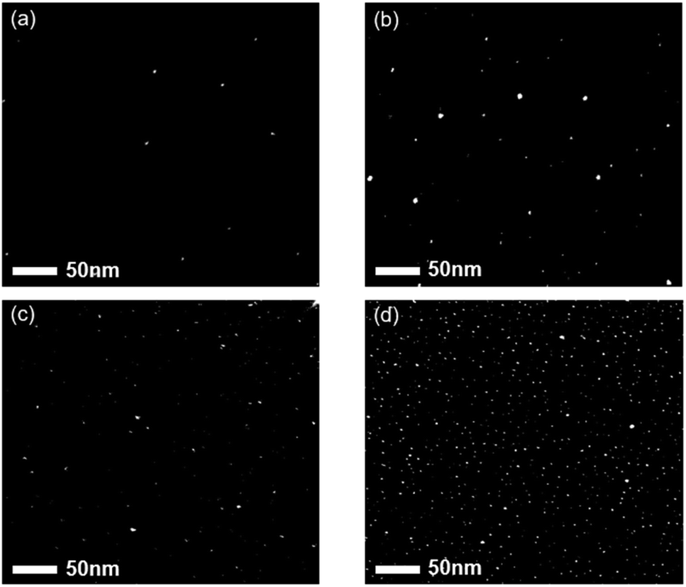 | ||
| Fig. 2 STEM images of nanoparticles captured for 10 s (a) on the SiO membrane on the quartz holder, (b) on the SiO membrane on the stainless-steel holder, (c) on the carbon membrane on the quartz holder, and (d) on the carbon membrane on the stainless steel-holder at the capture temperature of 600 °C and the filament temperature of 2000 °C at the gas mixture of 3% CH4–97% H2. | ||
The average number densities of nanoparticles per μm2 were 65, 283, 390, and 2713 under the capture conditions shown in Fig. 2a–d, respectively, and the average size of nanoparticles was approximately 3.1, 3.3, 3.2, and 3.2 nm. The SiO membrane is an electrical insulator. The average number density of nanoparticles on the SiO membrane using the grounded stainless holder (Fig. 2b) was four-fold larger than that on the floating quartz holder (Fig. 2a). The average number density of nanoparticles on the carbon membrane of the grounded holder (Fig. 2d) was seven-fold larger than that on the floating holder (Fig. 2c). In contrast, the average number densities of nanoparticles on the carbon membrane were 6-fold and 9.6-fold larger than those on the SiO membrane using the quartz and stainless steel holders, respectively. These results indicate that the negatively charged nanoparticles have difficulty in landing on the insulating surface, which is attributed to Coulomb repulsion between the negatively charged nanoparticles and negatively charged surface.
Similar experiments were carried out with the gas mixture of 1% CH4–99% H2; however, the SiO membrane was much more damaged at the capture temperature of 600 °C with 1% CH4–99% H2 than with 3% CH4–97% H2. Moreover, the carbon membrane was completely etched away with the 1% CH4–99% H2 gas mixture. Thus, nanoparticle capture at 1% CH4–99% H2 failed at 600 °C. As such, the capture temperature was reduced to 300 °C for nanoparticle capture using the carbon membrane. The average size of the nanoparticles was ∼10 nm, which indicated coalescence of the primary nanoparticles. HR-TEM observations revealed that those nanoparticles had an onion-like structure, implying that nanoparticles undergo a structural change in the gas phase or on the amorphous carbon membrane.
Therefore, we used a graphene membrane at 600 °C to capture nanoparticles generated with 1% CH4–99% H2. Fig. 3a and b show TEM images of nanoparticles captured on the graphene membrane of the Cu TEM grid; the capture time was 10 s at the filament temperature was 2000 °C using 1% CH4–99% H2. In Fig. 3a, the graphene membrane on the Cu grid was placed on the quartz holder in the floating condition. In Fig. 3b, the graphene membrane was placed on the stainless steel holder in the grounded condition. The average sizes of nanoparticles captured in the floating and grounded conditions were, respectively, 3.99 and 3.87 nm. The average number density of the nanoparticles captured in the grounded condition was 7.9 × 10³ per μm2, almost five times larger than that in the floating condition (1.6 × 10³ per μm2). These results confirmed again that the build-up of negative charges on the floating membrane creates a repulsive Coulomb interaction with the negatively charged nanoparticles.
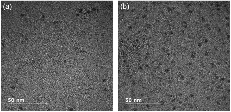 | ||
| Fig. 3 TEM images of nanoparticles captured on the graphene membrane of the TEM Cu grid (a) on the quartz holder and (b) on the stainless-steel holder at the capture temperature of 600 °C and the gas mixture of 1% CH4–99% H2. | ||
To compare the crystal structure of the nanoparticles captured in floating and grounded conditions, we examined the structures using both HR-TEM and unit cell structure of various carbon allotropes in Fig. S1.† Four carbon allotropes were identified: i-carbon, hexagonal diamond, n-diamond, and cubic diamond. Comparison of the experimentally observed d-spacing values with those reported for cubic diamond, n-diamond, hexagonal diamond, and i-carbon was summarized in Table S1.† The nanoparticles in Fig. 4a were captured on the graphene membrane, which was placed on the quartz holder for 10 s at 600 °C with a filament temperature of 2000 °C and gas mixture of 1% CH4–99% H2. The FFT image in Fig. 4a shows single-crystalline cubic diamond along the 〈110〉 zone axis. HR-TEM and FFT images show the two (111) planes of cubic diamond (Fd![[3 with combining macron]](https://www.rsc.org/images/entities/char_0033_0304.gif) m) and the d-spacing of 2.06 Å corresponding to the (111) plane. In addition, the lattice angle of 70° in Fig. 4a, between the two (111) planes, matches that of cubic diamond (JCPDS no. 6-0675). The conditions used to capture the nanoparticles shown in Fig. 4b were the same as those used to capture the nanoparticles in Fig. 4a. The FFT image in Fig. 4b shows single-crystalline n-diamond along the 〈110〉 zone axis. HR-TEM and FFT images show the (111) and (200) lattice planes of n-diamond; the d-spacing value of 1.79 Å corresponds to the forbidden diamond reflection (200) plane. The lattice angles of 70° and 54° in Fig. 4b are the angles, respectively, between the two (111) planes and between the (111) and (200) planes, representing n-diamond. A lattice angle of 54° between the (111) and (200) planes was observed for the n-diamond structure. It should be noted that cubic and hexagonal diamonds do not have a lattice angle of 54° between the (111) and (200) planes (JCPDS no. 43-1104).
m) and the d-spacing of 2.06 Å corresponding to the (111) plane. In addition, the lattice angle of 70° in Fig. 4a, between the two (111) planes, matches that of cubic diamond (JCPDS no. 6-0675). The conditions used to capture the nanoparticles shown in Fig. 4b were the same as those used to capture the nanoparticles in Fig. 4a. The FFT image in Fig. 4b shows single-crystalline n-diamond along the 〈110〉 zone axis. HR-TEM and FFT images show the (111) and (200) lattice planes of n-diamond; the d-spacing value of 1.79 Å corresponds to the forbidden diamond reflection (200) plane. The lattice angles of 70° and 54° in Fig. 4b are the angles, respectively, between the two (111) planes and between the (111) and (200) planes, representing n-diamond. A lattice angle of 54° between the (111) and (200) planes was observed for the n-diamond structure. It should be noted that cubic and hexagonal diamonds do not have a lattice angle of 54° between the (111) and (200) planes (JCPDS no. 43-1104).
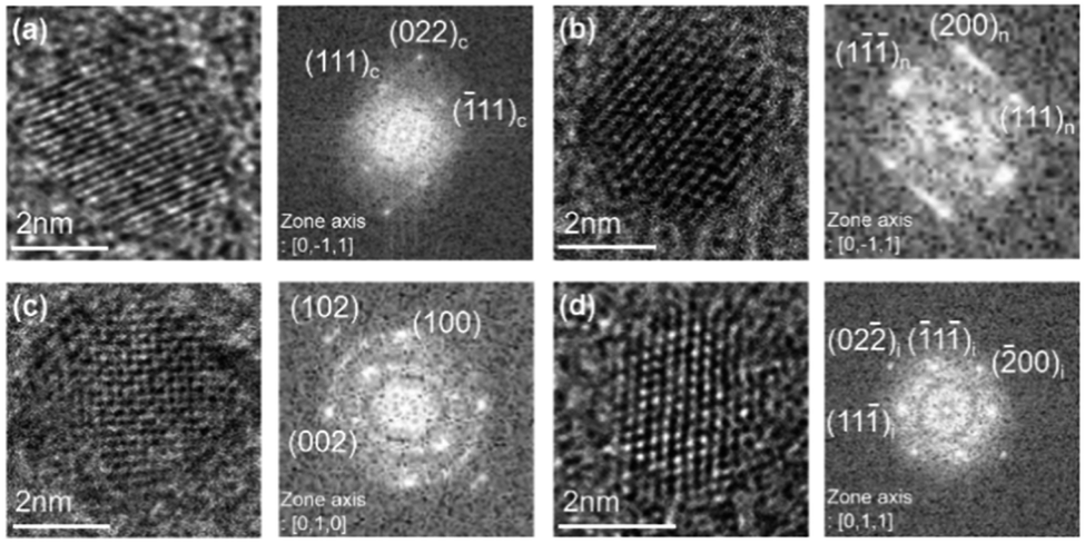 | ||
| Fig. 4 HRTEM and FFT images of (a) cubic diamond (JCPDS6-0675), (b) n-diamond (JCPDS43-1104) captured on the floating graphene membrane and (c) hexagonal diamond (JCPDS19-0268) and (d) i-carbon (29) captured on the grounded graphene membrane. | ||
The nanoparticles shown in Fig. 4c were captured on a graphene membrane placed on the stainless-steel holder; the other conditions were the same as those used to obtain the results shown in Fig. 4a. The FFT image in Fig. 4c shows single-crystalline hexagonal diamond along the 〈100〉 zone axis with d-spacings of 2.19, 2.07, and 1.51 Å, which were assigned to the (100), (002), and (102) lattice planes of hexagonal diamond, respectively. The d-spacing values of 2.19 Å and 1.51 Å are specific to hexagonal diamond. The lattice angles of 90° and 46° in Fig. 4b were attributed to the angles between the (100) and (002) planes and between the (100) and (102) planes, respectively, of hexagonal diamond (JCPDS no. 19-0268).
The conditions used to capture the nanoparticle shown in Fig. 4d were the same as those shown in Fig. 4c. The FFT image in Fig. 4d shows single-crystalline cubic-phase diamond along the 〈100〉 zone axis. The nanoparticle contained three lattice planes with d-spacings of 2.42, 2.10, and 1.50 Å, corresponding to (111), (200), and (220), respectively, of the cubic phase with a lattice parameter of 4.2 Å. The lattice angles of 70°, 54°, and 35° in Fig. 4d were also assigned, respectively, to the angles between the two (111) planes, between the (111) and (200) planes, and between the (111) and (220) planes of i-carbon. The i-carbon nanoparticles showed variation in the d-spacing value in the range of 2.36–2.54 Å; the lattice parameter of i-carbon had a range of 4.1–4.4 Å.29,30
We also investigated how the nanoparticles captured with the graphene membrane on the quartz holder differ from those captured on the same membrane on the stainless steel holder. For this, we analyzed the phase of the captured nanoparticles. Fig. 5 shows the frequencies of the d-spacing values of nanoparticles captured at 600 °C on the graphene membranes in the floating and grounded conditions, using the gas mixture of 1% CH4–99% H2 at a filament temperature of 2000 °C. The frequencies shown in Fig. 5 were determined from 150 d-spacing values from ∼100 nanoparticles for each membrane. The frequency of the d-spacing value in Fig. 5 should be closely related to the X-ray diffraction (XRD) intensity of the polycrystal; thus, this value can be used to roughly estimate the phase fraction of the nanoparticles.29–33
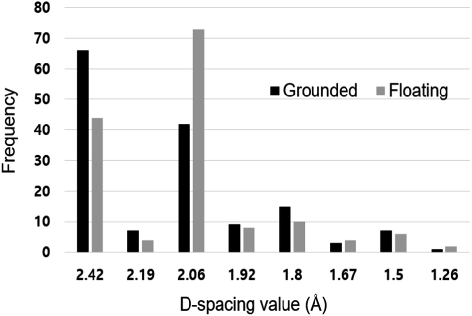 | ||
| Fig. 5 Frequency of d-spacing values of nanoparticles captured at 1% CH4–99% H2. The data were obtained by analyzing 150 d-spacing values out of ∼100 nanodiamonds for each membrane. | ||
The d-spacing values were analyzed according to the values reported by the JCPDS for the carbon allotrope. We assumed that the observed d-spacing would correspond to those of the JCPDS, if the d-spacing values were within ∼3%. For the nanoparticles captured on the grounded holder, the frequencies of the d-spacing values of 2.42 and 2.06 Å were 58 and 43, respectively. For the nanoparticles captured on the floating holder, however, the frequencies of 2.42 and 2.06 Å were 37 and 73, respectively.
The d-spacing of 2.42 Å belongs to i-carbon, whereas the d-spacing of 2.06 Å belongs to cubic diamond or n-diamond. Therefore, the higher frequency of 2.06 Å than 2.42 Å in the floating condition in Fig. 5 indicates that cubic diamond or n-diamond is a major phase, whereas i-carbon is a minor phase. Similarly, the lower frequency of 2.06 Å than that of 2.42 Å in the grounded condition indicates that i-carbon is a major phase, whereas cubic diamond or n-diamond is a minor phase.
Peng et al.31 confirmed that n-diamond contained sp3 bonded carbon content of approximately 95%, whereas the i-carbon appeared as predominately sp2 bonded. Negative charge built up on the graphene membrane would be expected to be much greater in the floating condition than in the grounded condition. According to Fig. 5, such a build-up of negative charge seems to promote the stability of cubic diamond or n-diamond over that of i-carbon. The build-up of negative charges or electrons on the grounded membrane would be much less than that on the floating membrane. Such a low charging state on the grounded membrane may be sufficient to change the nanoparticles from cubic diamond or n-diamond to i-carbon.
In a previous study, Hwang et al.34 observed that a diamond film formed on a Si substrate, and porous skeletal soot particles formed on an Fe substrate under the same HFCVD processing conditions; further, they observed that the soot continued to grow on the grounded Fe substrate, while diamond crystals grew on the initially formed soot on the floating Fe substrate after 2 h of deposition. To explain the results, they suggested that negatively charged diamond nanoparticles are generated in the gas phase, and that these particles maintained diamond stability upon landing on the Si substrate. In contrast, diamond stability was lost, and diamond transformed to graphite, after losing charge on the Fe substrate. Based on ab initio calculations, Lai and Barnard21 confirmed that a phase transition occurs between bucky-diamonds and onion-like structures, depending on the sign of extra charge. They suggested that negative charging of nanoparticles stabilizes the dangling bonds of carbon atoms at the surface. Saturated dangling bonds lead to the disappearance of reconstructed and graphitised layers at the surface. Park et al.22 also showed, based on ab initio calculations, that negative charging of a cluster containing 165 carbon atoms stabilizes the diamond structure over the graphite structure.
It is well known that the crystal structure of nanoparticles is strongly related to their size. Surface stress affects the stability of diamond nanoparticles of 1–3.3 nm, including through delamination (graphitization) of the (111) surface to form fullerene and onion-like structures.35–38 Given that the different structure of nanoparticles between floating and grounded conditions may arise from the size difference, we measured the size distribution of nanoparticles.
Fig. 6a and b show the size distribution of nanoparticles captured on floating and grounded membranes, respectively. We analyzed 100 nanoparticles on each membrane. The 100 nanoparticles on the floating membrane had an average size of 3.99 ± 0.16 nm with 95% confidence. On the grounded membrane, the 100 nanoparticles had an average size of 3.87 ± 0.15 nm. The size distribution of the nanoparticles may affect the fraction of the specific carbon allotrope.38 However, Fig. 6 shows that nanoparticles captured under floating and grounded conditions have similar size distributions. Notably, Fig. 5 shows that the crystal structure depends strongly on the condition (floating vs. grounded). These results imply that the difference in crystal structure of nanoparticles is attributable to charging, as opposed to nanoparticle size.
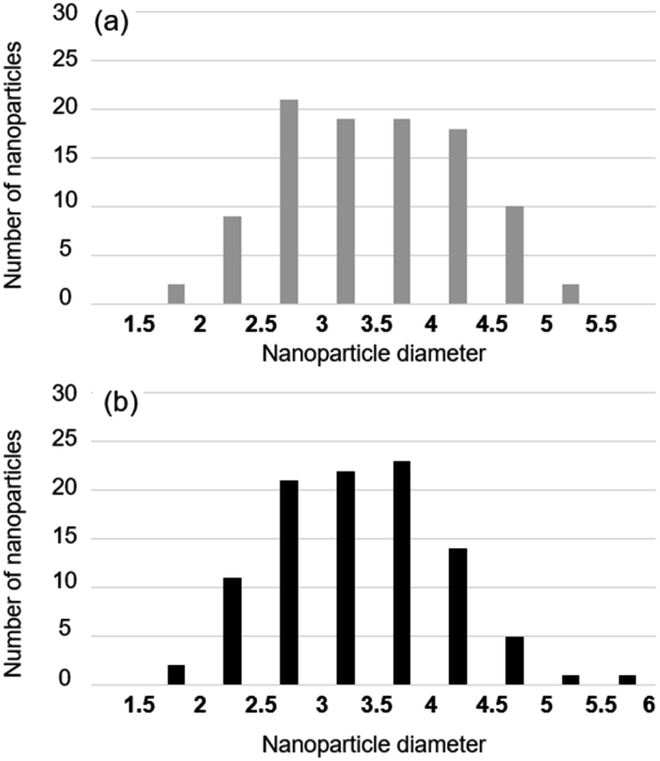 | ||
| Fig. 6 Size distribution of nanoparticles captured on the graphene membrane (a) on the quartz holder and (b) on the stainless-steel holder. | ||
The size of the observed nanoparticles was 2–5 nm. The (111) surface of nanoparticles in this size range should be delaminated to form the bucky-diamonds, which contained chemically inert diamond core and the fullerene-like shell.22 However, the shell structure at the surface of nanoparticles was not observed as shown in Fig. 4 and other nanoparticles. Based on the previous ab initio studies on the relationship between the negative charge and the structure of diamond, the surface of the nanoparticles observed in this study seems to be stabilized by negative charge. However, there is no report on the mechanism of phase transition from the cubic-diamond to i-carbon when diamond nanoparticles lose their negative charge.
To compare the deposition behavior between floating and grounded conditions, a bare Si substrate was used for deposition at 950 °C for 8 h under the same processing conditions as those where the nanoparticles were captured. Because a bare Si substrate was used without pretreatment, isolated diamond particles formed instead of diamond films. For floating of the Si substrate, we inserted a 1 mm thick sapphire plate between the Si substrate and the stainless steel holder; to ground the Si substrate, the substrate was placed directly onto the stainless steel holder. Due to the thermal conductivity and heat capacity of the sapphire plate, the temperature of the Si substrate on the plate was slightly higher than that on the stainless-steel holder. To equalize the temperatures of the Si substrates, the distance between the filament and substrate was adjusted.
Fig. 7a and b show FE-SEM images of the diamond particles deposited on the bare Si substrate under floating and grounded conditions, respectively. The average number density of diamonds deposited in the floating condition was 142 per cm2, whereas in the grounded condition it was 445 per cm2. The number density in the grounded condition was almost three-fold larger than that in the floating condition, similar to the result whereby the number density of nanoparticles captured under grounded conditions is larger than that under floating conditions, as shown in Fig. 2 and 3.
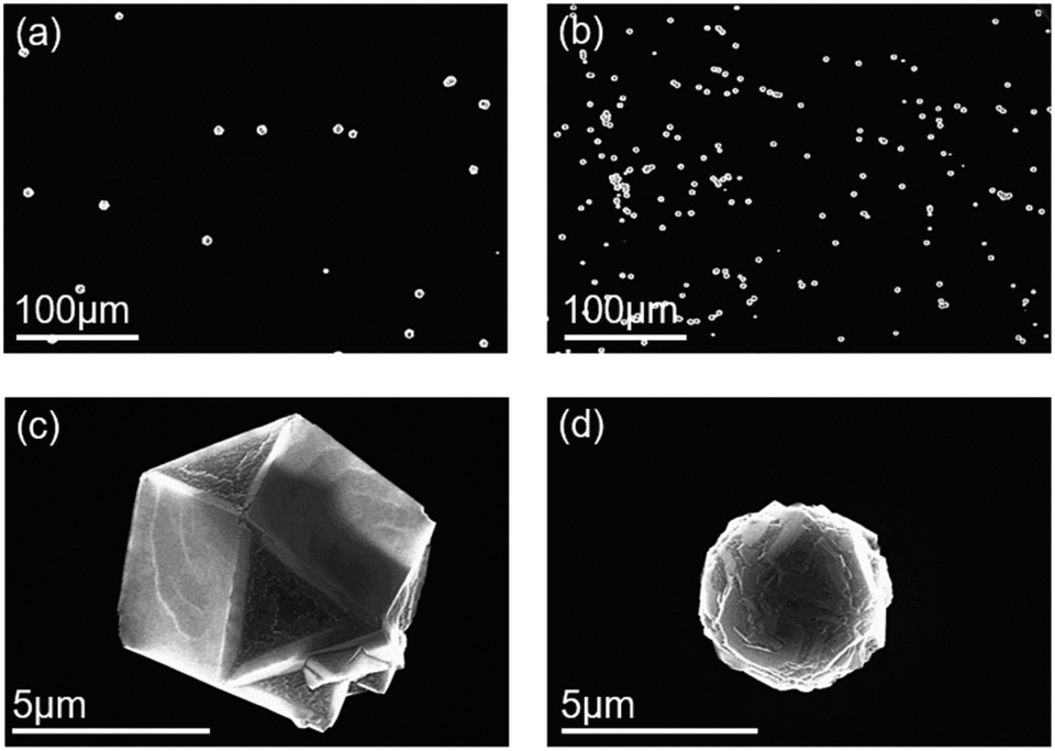 | ||
| Fig. 7 FESEM images of diamonds deposited for 8 h on the bare silicon substrate (a) on the sapphire plate on the stainless-steel holder and (b) on the stainless-steel holder. (c) and (d) are magnified images of a diamond particle of (a) and (b), respectively. | ||
Fig. 7c and d are higher magnification FE-SEM images of Fig. 7a and b, respectively. The diamond particle in Fig. 7c deposited under a floating condition has a cuboctahedron shape with well-defined facets, whereas that in Fig. 7d deposited under a grounded condition has an overall spherical shape and is partially covered with crystalline facets. The size of the diamond particles deposited under a floating condition was larger than that obtained under a grounded condition. Each particle was analyzed by a micro Raman spectrometer with a spot size of 1 μm. Fig. 8a and b show the Raman spectra of the particles deposited in the floating and grounded conditions, respectively. The Raman spectra in Fig. 8a show a sharp peak at 1332 cm−1, which indicates diamond. However, the Raman spectrum in Fig. 8b shows broadening of the G-band.39,40 The relative intensity (ID/IG) of the particle deposited in the floating condition was higher than that in the grounded condition.
 | ||
| Fig. 8 Raman spectra of deposited diamond particles deposited (a) on the floating substrate (Fig. 7a) and (b) on the grounded substrate (Fig. 7b). | ||
Comparing the crystal structure of the deposited particles and the Raman peaks with the crystal structure of captured nanoparticles, the high frequency associated with the 2.06 Å d-spacing in Fig. 5 is related to the intensity of the 1332 cm−1 diamond Raman peak, and that corresponding to the 2.42 Å d-spacing corresponds to Raman broadening of the graphite Raman peak.41,42 Fig. 7c and d show that the size of particles deposited in the floating condition is larger than that of particles deposited in the grounded condition. In this case, the particles deposited under a grounded condition would be easily etched by atomic hydrogen due to their graphite-like structure,43,44 resulting in a smaller size.
As to the growth mechanism of diamond films or particles by HFCVD, Hwang27 suggested a theory of charged nanoparticles (TCN), where diamond films or particles grow by the building block of the gas phase nuclei. According to this theory, nanoparticles shown in Fig. 4 are the building block of diamond particles shown in Fig. 7. More specifically, cubic diamond and n-diamond shown, respectively, in Fig. 4a and b would mainly contribute to the growth of high-quality faceted diamond particles shown in Fig. 7c. And i-carbon shown in Fig. 4d would mainly contribute to the growth of partially-faceted and ball-like diamond particles shown in Fig. 7d.
4. Conclusions
The number density of nanoparticles captured in the grounded condition was much larger than that in the floating condition. Nanoparticles captured in the floating condition consisted mainly of cubic diamond and n-diamond, whereas those captured in the grounded condition consisted mainly of i-carbon. Diamond particles deposited in the floating condition displayed an octahedral shape with well-developed facets, and had a high-intensity 1332 cm−1 diamond Raman peak, whereas those deposited in the grounded condition showed an overall spherical shape and were partially covered with crystalline facets with a broad G-band Raman peak. These results indicate that negative charging stabilizes the diamond structure of nanoparticles, which contributes to the deposition of crystalline diamond with well-developed facets.Conflicts of interest
There are no conflicts to declare.Acknowledgements
This work was partially supported by the National Research Foundation of Korea (NRF) grant funded by the Korea government (MSIT) (No. 2020R1A5A6017701), Global Frontier Program through the Global Frontier Hybrid Interface Materials (GFHIM) of the National Research Foundation of Korea (NRF) funded by the Ministry of Science, ICT & Future Planning (MSIP) (No. 2013M3A6B1078874) and This work was also supported by the Asian Office of Aerospace Research and Development (AOARD) (FA2386-15-1-4067).References
- F. P. Bundy, H. T. Hall, H. M. Strong and R. H. Wentorf, Nature, 1955, 176, 51–55 CrossRef CAS.
- C. V. Deshpandey and R. F. Bunshah, J. Vac. Sci. Technol., A, 1989, 7, 2294–2302 CrossRef CAS.
- J. C. Angus, H. A. Will and W. S. Stanko, J. Appl. Phys., 1968, 39, 2915–2922 CrossRef CAS.
- S. M. Pimenov, G. A. Shafeev, A. A. Smolin, V. I. Konov and B. K. Vodolaga, Appl. Surf. Sci., 1995, 86, 208–212 CrossRef CAS.
- T. L. Daulton, M. A. Kirk, R. S. Lewis and L. E. Rehn, Nucl. Instrum. Methods Phys. Res., Sect. B, 2001, 175, 12–20 CrossRef.
- V. V. Danilenko, Phys. Solid State, 2004, 46, 595–599 CrossRef CAS.
- V. Y. Dolmatov, Russ. Chem. Rev., 2007, 76, 339–360 CrossRef CAS.
- Y. Xing and L. Dai, Nanomed, 2009, 4, 207–218 CrossRef CAS.
- C. Y. Cheng, E. Perevedentseva, J. S. Tu and P. H. Chung, et al., Appl. Phys. Lett., 2007, 90, 163903 CrossRef.
- D. Pech, M. Brunet, H. Durou and P. Huang, et al., Nat. Nanotechnol., 2010, 5, 651–654 CrossRef CAS.
- J. P. Boudou, P. A. Curmi, F. Jelezko and J. Wrachtrup, et al., Nanotechnol, 2009, 20, 235602 CrossRef.
- H. W. Whitlock and M. W. Siefkien, J. Am. Chem. Soc., 1968, 90, 4929–4939 CrossRef CAS.
- T. M. Grund, P. R. Schleyer, P. H. Gund and W. T. Wipke, J. Am. Chem. Soc., 1975, 97, 743–751 CrossRef.
- J. E. Dahl, S. G. Liu and R. M. K. Carlson, Science, 2003, 299, 96–99 CrossRef CAS.
- J. C. Angus and C. C. Hayman, Science, 1988, 241, 913–921 CrossRef CAS.
- P. K. Bachmann, D. Leers and H. Lydtin, Diamond Relat. Mater., 1991, 1, 1021–1034 CrossRef.
- W. R. L. Lambrecht, C. H. Lee, B. Segall and J. C. Angus, et al., Nature, 1993, 364, 607–610 CrossRef CAS.
- D. M. Gruen, S. Liu, A. R. Krauss, J. Luo and X. Pan, Appl. Phys. Lett., 1994, 64, 1502 CrossRef CAS.
- A. V. Palnichenko, A. M. Jonas, J. C. Charlier, A. S. Aronin and J. P. Issi, Nature, 1999, 402, 162–165 CrossRef CAS.
- M. Yoshimoto, K. Yoshida, H. Maruta and Y. Hishitani, et al., Nature, 1999, 399, 340 CrossRef CAS.
- L. Lai and A. S. Barnard, J. Mater. Chem., 2012, 22, 13141 RSC.
- N. J. Park, S. G. Park, N. M. Hwang and J. S. Ihm, et al., Phys. Rev. B: Condens. Matter Mater. Phys., 2004, 69, 195411 CrossRef.
- N. M. Hwang, J. H. Hahn and D. Y. Yoon, J. Cryst. Growth, 1996, 162, 55–68 CrossRef CAS.
- J. D. Jeon, C. J. Park, D. Y. Kim and N. M. Hwang, J. Cryst. Growth, 2000, 213, 79–82 CrossRef CAS.
- I. D. Jeon, C. J. Park, D. Y. Kim and N. M. Hwang, J. Cryst. Growth, 2001, 223, 6–14 CrossRef CAS.
- J. W. Park, K. S. Kim and N. M. Hwang, Carbon, 2016, 106, 289–294 CrossRef CAS.
- N. M. Hwang, Non-Classical Crystallization of Thin Films and Nanostructures in CVD and PVD Processes, Springer, Dordrecht, 1st edn, 2016, ch. 5–6, pp. 101–158 Search PubMed.
- J. D. Watts and R. J. Bartlett, J. Chem. Phys., 1992, 96, 6073–6084 CrossRef CAS.
- H. Vora and T. J. Moravec, J. Appl. Phys., 1981, 52, 6151–6157 CrossRef CAS.
- H. Y. Kim, D. S. Kim, K. S. Kim and N. M. Hwang, Nanomaterials, 2020, 10, 2504 CrossRef CAS.
- J. L. Peng, J. O. Orwa, B. Jiang, S. Prawer and L. A. Bursill, Int. J. Mod. Phys. B, 2001, 15, 3107–3123 CrossRef CAS.
- H. Hirai and K. Konda, Proc. Jpn. Acad., Ser. B, 1991, 67, 22–26 CrossRef CAS.
- F. P. Bundy and J. S. Kasper, J. Chem. Phys., 1967, 46, 3437 CrossRef CAS.
- N. M. Hwang, J. H. Hahn and D. Y. Yoon, J. Cryst. Growth, 1996, 162, 55–68 CrossRef CAS.
- V. L. Kuznetsov, I. L. Zilberberg, Yu. V. Butenko and A. L. Chuvilin, J. Appl. Phys., 1999, 86, 863–870 CrossRef CAS.
- N. W. Winter and F. H. Ree, J. Comput.-Aided Mater. Des., 1998, 5, 279–294 CrossRef CAS.
- A. S. Barnard, S. P. Russo and I. K. Snook, Diamond Relat. Mater., 2003, 12, 1867–1872 CrossRef CAS.
- A. S. Barnard, S. P. Russo and I. K. Snook, Philos. Mag. Lett., 2003, 83, 39–45 CrossRef CAS.
- P. K. Chu and L. Li, Mater. Chem. Phys., 2006, 96, 253–277 CrossRef CAS.
- S. Prawer and R. J. Nemanich, Phil. Trans. R. Soc., 2004, 362, 2537–2565 CrossRef CAS.
- L. Abello, G. Lucazeau, B. Andre and T. Priem, Diamond Relat. Mater., 1992, 1, 512–518 CrossRef CAS.
- A. C. Ferrari and J. Robertson, Phys. Rev. B: Condens. Matter Mater. Phys., 2000, 61, 14095 CrossRef CAS.
- C. M. Donnelly, R. W. McCullough and J. Geddes, Diamond Relat. Mater., 1997, 6, 787–790 CrossRef CAS.
- C. Kanai, K. Watanabe and Y. Takakuwa, Phys. Rev. B: Condens. Matter Mater. Phys., 2001, 63, 235311 CrossRef.
Footnote |
| † Electronic supplementary information (ESI) available: (1) Unit cell of various allotropes of diamond; (2) comparison of observed d-spacing values. See DOI: 10.1039/d0ra09649k |
| This journal is © The Royal Society of Chemistry 2021 |